HAL Id: hal-02860979
https://hal.univ-lorraine.fr/hal-02860979
Submitted on 10 Feb 2021
HAL is a multi-disciplinary open access
archive for the deposit and dissemination of
sci-entific research documents, whether they are
pub-lished or not. The documents may come from
teaching and research institutions in France or
abroad, or from public or private research centers.
L’archive ouverte pluridisciplinaire HAL, est
destinée au dépôt et à la diffusion de documents
scientifiques de niveau recherche, publiés ou non,
émanant des établissements d’enseignement et de
recherche français ou étrangers, des laboratoires
publics ou privés.
Optically Induced Phase Change for Magnetoresistance
Modulation
Guodong Wei, Xiaoyang Lin, Zhizhong Si, Dong Wang, Xinhe Wang, Xiaofei
Fan, Kun Deng, Kaï Liu, Kaili Jiang, Na Lei, et al.
To cite this version:
Guodong Wei, Xiaoyang Lin, Zhizhong Si, Dong Wang, Xinhe Wang, et al.. Optically Induced
Phase Change for Magnetoresistance Modulation. Advanced Quantum Technologies, Wiley, 2020,
�10.1002/qute.201900104�. �hal-02860979�
Optical methods for magnetism manipulation have been considered as a promising strategy for ultralow-power and ultrahigh-speed data storage and processing, which have become an emerging field of spintronics. However, a widely applicable and efficient method has rarely been demonstrated. Here, the strongly correlated electron material vanadium dioxide (VO2) is used to realize the optically induced phase change for control of the magnetism in NiFe. The NiFe/VO2bilayer heterostructure features appreciable modulations of elec-trical conductivity (32%), coercivity (37.5%), and magnetic anisotropy (25%). Further analyses indicate that interfacial strain coupling plays a crucial role in the magnetic modulation. Utilizing this heterostructure, which can respond to both optical and magnetic stimuli, a phase change controlled anisotropic mag-netoresistance (AMR) device is fabricated, and reconfigurable Boolean logics are implemented. As a demonstration of phase change spintronics, this work may pave the way for next-generation opto-electronics in the post-Moore era.
1. Introduction
With integrated circuit production approaching its physical limits, spintronics has become one of the most promising technologies for information storage and processing in the post-Moore era, owing to its superior properties, including non-volatility, high speed, and low power consumption.[1–3] The
Dr. G. Wei, Prof. X. Lin, Z. Si, Dr. X. Wang, X. Fan, K. Deng, Prof. N. Lei, Prof. W. Zhao
Fert Beijing Research Institute, School of Microelectronics & Beijing Advanced Innovation Center for Big Data and Brain Computing (BDBC) Beihang University
Beijing 100191, China
E-mail: [email protected]; [email protected] Prof. X. Lin, Prof. W. Zhao
Beihang-Goertek Joint Microelectronics Institute, Qingdao Research Institute
Beihang University Qingdao 266000, China Dr. D. Wang, Prof. Y. Chen
School of Physics, State Key Laboratory of Crystal Materials Shandong University
Jinan 250100, China
The ORCID identification number(s) for the author(s) of this article can be found under https://doi.org/10.1002/qute.201900104
DOI: 10.1002/qute.201900104
those achieved by local control meth-ods such as voltage-controlled magnetic anisotropy,[4,5] all-optical switching,[6,7]
multiferroic,[8,9] and ionic[10–12]
modula-tions, have already demonstrated great potential in device performance improve-ments and application revolutions.[13]
Meanwhile, optical devices with the ad-vances of high speed, wide bandwidth, and low loss have greatly promoted the modern communication industry.[14]
Com-bining the advantages of spintronic and opto-electronic devices may highly im-prove the energy conversion efficiency, increase the device speed, and diversify the functionalities.[15,16]In this sense, a strategy
to realize the optical control of magnetic characteristics can promote the integration of spintronic devices into optical systems and trigger emergent device applications.
Strong correlations between electrons enable extraordinary control of physical properties (e.g., magnetism and conductiv-ity) via different strategies (e.g., electric fields, magnetic fields, and stresses), which implies numerous possibilities for strongly correlated electron materials in various research fields, includ-ing high-temperature superconductors, 2D electron gas systems,
Prof. K. Jiang
State Key Laboratory of Low-Dimensional Quantum Physics
Department of Physics & Tsinghua-Foxconn Nanotechnology Research Center
Collaborative Innovation Center of Quantum Matter Tsinghua University
Beijing 100084, China Prof. K. Liu
State Key Laboratory of New Ceramics and Fine Processing, School of Materials Science & Engineering
Tsinghua University Beijing 100084, China Prof. S. Mangin
Institut Jean Lamour, UMR 7198 CNRS—Université de Lorraine F-54000 Nancy, France Prof. E. Fullerton
Center for Memory and Recording Research University of California San Diego 9500 Gilman Drive, La Jolla, CA 92093, USA
www.advancedsciencenews.com www.advquantumtech.com
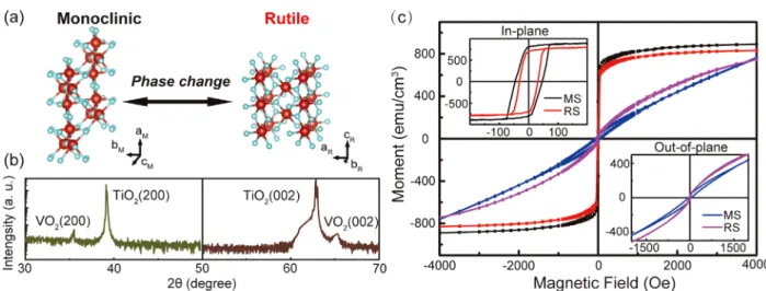
Figure 1. Phase change of VO2and characterization of the NiFe/VO2heterostructure. a) Schematic illustration of the reversible phase change of VO2 between monoclinic (M1) and rutile (R) lattice structures. b) XRD𝜃–2𝜃 scan of the NiFe/VO2 heterostructure grown on TiO2(100) and TiO2(001) substrates, suggesting epitaxial growth of the VO2layer and polycrystalline growth of the NiFe layer. c)M–H hysteresis loops of the NiFe (5 nm)/VO2 (20 nm)/TiO2(100) sample measured before and after the phase change of VO2(MS at 300 K and RS at 360 K). The magnetic field is applied perpendicular (data plotted as circles) and parallel (data plotted as squares) to the surface. The insets give the scanning results over small fields.
and next-generation spintronics.[17] As a representative strongly
correlated electron material, VO2 exhibits complex property
changes as it transforms from a low-temperature monoclinic (M1) insulator into a high-temperature rutile (R) metal at a criti-cal temperature around 340 K (Figure 1a).[18,19]The phase change
can also be induced by other methods such as the electrical gating,[20]optothermal heating (Figure S1, Supporting
Informa-tion) or even photonic effect,[21] which has greatly enriched its
device applications. The sub-ps optically induced phase change further endows VO2-related devices with the feature of
ultra-fast speed.[22,23]Therefore, a phase change-based spintronic
de-vice may reform the magnetism modulation strategy and enable emergent optical-spintronic device applications.
In this work, we study the optical control of magnetism in NiFe/VO2heterostructures combining a strongly correlated
elec-tron material with a magnetic material. Appreciable and re-versible modulations of the electrical conductivity (32%), coerciv-ity (37.5%) and magnetic anisotropy (25%) have been achieved in these heterostructures during the phase change of VO2. Further
analyses indicate that interfacial strain coupling plays a crucial role in this magnetic property modulation. Based on these fea-tures, the heterostructures are further used to demonstrate mul-tiresistance states and implement devices with reconfigurable logics. As an optical magnetism modulation strategy, the colli-sion and blending of strongly correlated electron materials and spintronic materials may pave the way for next-generation opto-electronics.
2. Magnetism Modulation Induced by VO
2Phase
Change
The NiFe/VO2 bilayer heterostructure used in this work is
pre-pared by two steps. VO2is first epitaxially deposited on TiO2
sub-strates by pulsed laser deposition (PLD), and NiFe is deposited at room temperature by magnetron sputtering. Figure 1b shows the X-ray diffraction (XRD) results of the heterostructure samples.
The (200) and (002) peaks of VO2are detected on the samples
with TiO2(100) and (001) substrates, respectively. The spectrum
shows no distinct characteristic peaks of NiFe, which indicates the amorphous feature of NiFe.
To investigate the magnetic characteristics modulated by the phase change, hysteresis loops of a NiFe (5 nm)/VO2 (20 nm)
sample grown on a TiO2 (100) substrate are measured for both
the monoclinic state (MS, 300 K) and rutile state (RS, 360 K) of VO2using a Superconducting Quantum Interference Device
(SQUID) magnetometer. As illustrated in Figure 1c, obvious anisotropy can be observed between the results with an in-plane and out-of-plane magnetic field applied. After the VO2 phase
change, the saturation magnetization (MS) of the heterostructure decreases from 898 to 840 emu cm–3, (i.e., a change of 6.5%,
cal-culated asMS difference divided by its original value). The in-sets show scanning results obtained within a small region, from which the shrinking of the coercive and saturation fields can be detected. Remarkably, the decrease is more obvious out of plane, enhancing the squareness of the curve around the zero field. The coercive field (HC) decreases from 72 to 45 Oe, (i.e., shows a change of 37.5%, calculated asHCdifference divided by its
orig-inal value). Generally, a temperature increase will not result in such a large change imbalance betweenHCandMS. Further dis-cussion, which will be given in the third section, proves that this variation is different from a mere thermal effect. After excluding the magnetic contribution of VO2single layer[24](Figure S1c,
Sup-porting Information), it is reasonable to believe that the effect is mainly caused by the phase change of VO2-induced modulation
on NiFe. It is noteworthy that the phase change temperature of VO2can be tuned from 300 to nearly 400 K by methods like
dop-ing or substrate stress, which will benefit its device application.[25]
To further explore this modulation effect, the magnetic param-eters of the heterostructure before and after the phase change are determined and summarized in Table 1. The uniaxial mag-netic anisotropy (Ku) can be derived from the in-plane and
out-of-plane hysteresis results,[26]which increases from−3.55 × 10⁶
dicular magnetic anisotropy. The bulk crystalline anisotropy is negligible because of the amorphous characteristic of the NiFe film. Then, the interfacial magnetic anisotropy can be calcu-lated as Ki = (Ku+ 2𝜋MS2)t, which increases from 0.755 to
0.885 erg cm–2. These results indicate the possibility of
re-alizing an interfacial perpendicular magnetic anisotropy en-hancement in other similar heterostructures, which is highly desirable for high-density and nonvolatile magnetic storage systems.[26,28]
After showing the magnetism modulation effect achieved through the phase change of VO2, we then focus on realizing
an optically controlled magnetic modulation by the optothermal effect. To achieve this goal, a laser beam (wavelength 660 nm) is used to trigger the phase change. Figure 2a gives the hys-teresis loops of the sample under different illumination power measured by an in situ longitudinal magneto-optic Kerr ef-fect (MOKE) magnetometer. An obvious modulation effect can be detected in the power change process, which verifies the
suring current (100 µA), the resistance shows a “roller coaster” behavior (inset of Figure 2c). The change rates of the resistance decrease from 32% to almost 0% (calculated as resistance differ-ence divided by its original value) as the measuring current is increased. Different from the behavior of ordinary metals, this complex resistance variation can be explained as the competition between the temperature dependent resistance of the magnetic metal and the insulator-to-metal transition induced by the VO2
phase change. Normally, illumination will increase the resistance of the NiFe; while the phase change from insulator to metal will reduce the resistance of VO2. Within the temperature region
de-termined by light illumination and electrical Joule heating, the different resistance-temperature characteristics can thus result in the aforementioned behaviors. As shown in Figure 2c, a small current of 1 µA will then be adopted to study the magnetoresis-tance controlled by the phase change.
Figure 2d–2f gives the magnetoresistance curves of the device under different illumination power. One obvious variation in this
Figure 2. Optically controlled magnetoresistance measurements. a) The hysteresis loops of the sample with different illumination power. b) Schematic
drawing of the PCAMR device. Direction of the applied magnetic fields,H, are also presented. c) The device resistance change measured with varied
applied current under increasing illumination power. d–f) Comparison of the magnetoresistance of the NiFe (5 nm)/VO2(20 nm)/TiO2(100) device without (d) and with the illumination of 1 W/cm2(e) and 1.6 W/cm2(f) red light.
www.advancedsciencenews.com www.advquantumtech.com
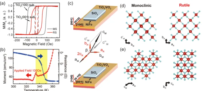
Figure 3. Interfacial strain analysis and characterization of magnetism modulation. a) Kerr signals of the NiFe/VO2heterostructure grown on differ-ent substrates with magnetic field applied in-plane. TheHCchange between the MS and RS is 45% for the TiO2 (100) substrate and 25% for the TiO2 (001) substrate when the illumination power reaches 2 W cm–2. b) Temperature dependence of out-of-plane magnetization of the heterostruc-ture with a magnetic field of 100 Oe (the red line), and the resistance change of VO2from 300 to 360 K (the blue line). c) Strain analysis when the VO2phase change occurs. d and e) Schematic diagram of the VO2crystal lattice change of the (001) plane and (100) plane with regard to the rutile structure.
process is the shift in the “valley bottom” (i.e., from≈50 to 10 Oe at 1 W cm–2), which agrees with the modulation on the
coerciv-ity of the heterostructure (Figure 1 and Table 1). In this device, light and magnetic field can induce the insulator-to-metal tran-sition and AMR effects, which endows the device with optically controlled PCAMR feature. Such an effect may enable emergent device applications, which will be discussed in the last section of this paper.
3. Strain Analysis and Mechanism Explanation
To clarify the relationship between the magnetism modulation and the phase change of VO2, a series of further experiments are
carried out based on the heterostructure samples. As illustrated in Figure 3a, even though the change rates are different, an obvi-ous coercive field decrease can be observed for heterostructures grown on substrates with different crystal orientations. However, only faint deviations ofHCcan be detected for the pristine NiFe sample (Figure S2a, Supporting Information). These results sug-gest that the modulation effect is dominated by the phase change of VO2, rather than by a pure thermal effect of the NiFe layer.
The magnetization–temperature (M-T) dependence of the het-erostructure sample is then measured as illustrated in Figure 3b. The magnetization increase during the heating process is coordi-nated with the out-of-plane coercive field shrinking. Interestingly,
theM-T curve shows an abnormal valley in the temperature range
where the resistance of VO2drops intensely. This phenomenon
can be explained by the phase coexistence of the nonmagnetic layer (for example, the VO2layer in this work).[29,30]The uniform
phase change of VO2can enhance the magnetization in a gradual
way. However, if the phase change is nonuniform, there will be
boundaries forming between two different phases of VO2. The
NiFe crystal grains around these boundaries can then be consid-ered as localized magnetic defects and act as pinning centers for magnetic domain wall movements. Thus, the magnetization in-crease is blocked. As more boundaries form, the magnetization may even decrease until the two types of phases are equal. Conse-quently, a valley is formed in theM-T curve. The relatively broad
temperature range and the flat bottom of this valley also reflect the existence of lattice defects in the VO2film, which can be
con-firmed by the TEM results in the later session.
Further experimental evidence indicates that this modulation is an interfacial effect. For heterostructure samples epitaxially de-posited on various TiO2substrates (Figure 3a), the experimental
data show that the change inHC(in-plane) reaches 45% for TiO2
(100) but only 25% for TiO2(001) between the MS and RS. This
feature verifies that the modulation depends on the crystalline structure of the VO2 layer. Figure 3c shows the analysis of the
crystal axis conversion of VO2 during its phase change.[21]
Re-markably, a more appreciable change can be achieved with the VO2layer grown on the TiO2(100) substrate. On the TiO2(001)
substrate, the in-plane lattice constant changes are≈0.4% and 0.2% along the aRand bRdirections, respectively (Figure 3d). On
the TiO2 (100) substrate, the lattice constant is compressed by
≈0.8% along cR, and the change rate between bRand cMreaches
18.5% with an additional shear force caused by the angle decrease
of𝛽 from 122.6° to 90° (Figure 3e; Table S1, Supporting
Infor-mation). As a result, the interfacial strain effect is enhanced in the VO2/TiO2(100) sample. This analysis suggests that the
dif-ferent magnetism modulation mechanisms could be attributed to the different magneto-elastic effect induced by the struc-ture change, in other words, the interfacial strain coupling be-tween VO2and NiFe. To confirm this conjecture, the modulation
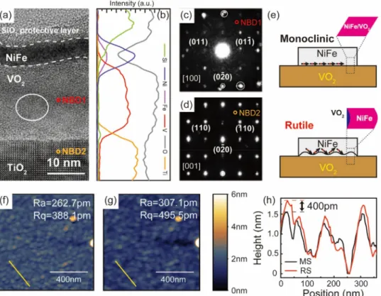
Figure 4. High-resolution transmission electron microscopy (HR-TEM) analysis of the NiFe/VO2heterostructure. a) Cross-section HR-TEM image of the NiFe/VO2heterostructure deposited on a TiO2(100) substrate. Some distortion of the crystal orientation can be detected in the VO2layer, as marked in this figure. b) Energy dispersive spectroscopy (EDS) analysis of different elements (Ti, O, V, Fe, Ni, and Si) in the heterostructure. c and d) Nanobeam electron diffraction (NBD) corresponding to NBD1 and NBD2 in (b). e) Schematic diagram of the heterostructure. When the crystal lattice changes, the increased interface roughness causes the spin, which is originally pinned in-plane, to turn to the out-of-plane direction. f and g) Atomic force microscope (AFM) results obtained at 300 and 355 K. The figures also give the average roughness (Ra) and the RMS roughness (Rq) data. A line scanning analysis along the yellow line is given in (h).
effect of heterostructures with different NiFe thicknesses are examined (Figure S2b,c, Supporting Information). The results show that the change inHC reaches 67% as the thickness de-creases to 3 nm and quickly drops to nearly 0% as the thick-ness increases to 10 nm. This result agrees with reports that the magneto-elastic coupling coefficient of NiFe is anomalously large for thicknesses below 5 nm.[31]Further engineering of this
inter-facial strain coupling effect in a NiFe/VO2heterostructure could
enable optimize modulation performance for various device ap-plications.
Based on the understanding that the magnetism modulation is mainly due to the interfacial strain, we then focus on the origin of the magnetism modulation caused by interfacial strain dur-ing the phase change.[32]Recent research has shown that by
en-gineering the surface, perpendicular or other types of magnetic anisotropy can be achieved in ultrathin magnetic films.[33]In our
phase change heterostructure, the lattice variation in the specific plane is quite large, which could lead to some periodic bending and spin reorientation of the NiFe film at the interface.[34]
As-suming that it mainly affects the domain wall motion, the mech-anism can be understood through a strain-induced anisotropy change.
The coercivityHCis determined by the domain wall energy:[35] Hc≈ (𝜕𝛾∕𝜕x)max∕
(
8𝜋MS) (1)
wherex is the position of the domain wall, MSis the saturation magnetization, and𝛾 is the domain wall energy. 𝛾 can be further written as:[36]
𝛾 = 4√A(K1+ 𝜆s𝜎
)
(2)
whereA is the exchange constant, K1is the crystal anisotropy,𝜆s is the magnetostriction coefficient, and𝜎 is the strain applied to the sample. Thus,HCdepends on the strain-induced variation in
the anisotropy.
As shown in Figure 4a,4b, the cross-section transmission elec-tron microscopy (cross-section TEM) results of the heterostruc-ture on a TiO2 (100) substrate verify the existence of thin-film
bending in the heterostructure and the absence of obvious inter-mixing at the interface. Some distortion of the crystal orientation in the VO2layer can be observed near the bending area (Figure 4a,
TEM image; Figure 4c,4d, nanobeam electron diffraction result). It may be caused by the VO2phase change when cooling from a
high growth temperature to room temperature. These structure features may further enhance the interface roughness of NiFe after the phase change, inducing reorientation of the spin from in-plane to out-of-plane[31](Figure 4e). The saturation
www.advancedsciencenews.com www.advquantumtech.com
Figure 5. Optically controlled multiresistance states and reconfigurable logics. a) Six different resistance states are realized using different illumination
power and magnetic field. b) Two resistance change curves are selected from Figure 2c to illustrate its dependence on measuring current (1 and 10 µA) when illumination (from 0.5 to 1.6 W cm–3) applied. The enlarged picture gives the operation settings of the reconfigurable logics. Light illumination (A) and applied current (B) are defined as two kinds of input signals. The corresponding 0 and 1 settings have been indicated by dashed and solid lines, respectively. Four resistance states achieved through the operation of A and B are summarized in the table. The value under same input signals can still be changed by the magnetic field, marked as the field on and field off states by dotted line. This figure also gives the reference resistance (RReference) to determine the output 0 and 1. c) The truth table of NOR and NAND operations. With magnetic field applied and removed, the logic can be reversibly switched between them. d) Circuit schematic to realize device concatenability.
the variation of the distances between individual magnetic grains caused by the bending interface structure.
To further confirm the existence of the phase change induced roughness change, AFM scanning is performed at 300 and 350 K (Figure 4f,4g). Compared to the sample surface morphology at the MS, an obvious roughness increase can be observed at the RS. Figure 4h provides the line scanning result, which shows that the height difference between the two states could reach 400 pm. These results are in agreement with the magnetic characteristic results, i.e., the increasedKuand enhanced squareness of the out-of-plane hysteresis loop.
4. Multiresistance Realization and Logic Function
Implementation
The magnetic sensitivity (Figure 2a) accompanied with the pho-tosensitivity (Figure 2c) in this heterostructure result in a highly controllable feature of its resistance, which can be adopted for different electronic applications.[37–39] Figure 5a demonstrates
an example of six different resistance states achieved via the synergistic control of the light illumination and magnetic field in the PCAMR device. Both the field and illumination enable the reversible, repeatable, and stable modulation of the device
four different states achieved through the operation of A and B. By setting an appropriate reference resistance (RReference) to
determine the output 0 and 1, a specific logic function is im-plemented. Notably, the resistance value can still be changed by the magnetic field, marked as the field on and field off states in this figure. So that the logic function can be reversibly switched by magnetic fields, for example, between NOR and NAND as shown in Figure 5c. Such a logic device can be used to per-form certain computational tasks, like circuit obfuscation as a hardware encryption to secure information. A circuit schematic is also given in Figure 5d, showing a possible strategy to meet the concatenability requirement of logic applications. Apart from the function demos we give above to show the possible applica-tions, it is reasonable to believe that the resistance of the device should be related to the power increasing and decreasing pro-cess in the hysteresis range. Such kind of history dependent fea-ture may be used to design beyond von-Neumann computing.[43]
Reports of beyond micrometer level optical integrations,[42]
to-gether with development of electrical spin manipulation meth-ods, such as spin-transfer-torque or spin-orbit-torque effects, may further give birth to a highly integrated phase change spintronic device.
5. Conclusion
To conclude, we have combined a strongly correlated electron material and a spintronic material to fabricate new artificial heterostructures in which the spintronic material is endowed with the optical modulation ability of the magnetic and electri-cal properties by a reversible phase change process. Changes of the electrical conductivity (32%), coercivity (37.5%), and mag-netic anisotropy (25%) have been observed in the NiFe/VO2
het-erostructure. Theoretical analyses and experimental evidence re-veal that the magneto-elastic coupling induced by appreciable interfacial strain (up to 18.5%) may be the origin of the mag-netism modulation. Further device implementations indicate that multiresistance states and reconfigurable logic functions can be achieved in the device. Our work, as a demonstration of opti-cally controlled phase change spintronics, may pave the way for next-generation opto-electronics.
heat source and SQUID (MPMS3, Quantum Design, Inc.) at room and high temperatures. The PCAMR devices were measured by normal four-terminal methods with Keithley 6221 and Keithley 2182 sourcing and mea-suring units, respectively. Meanwhile, an in-plane electromagnet (East Changing Co. China) provided magnetic fields with proper directions.
Supporting Information
Supporting Information is available from the Wiley Online Library or from the author.
Acknowledgements
G.W. and X.L. contributed equally to this work. The authors thank Huai-wen Yang, Zhaohao Wang, Jiwei Hou, Yuan Cao, and Runrun Hao for their help in device fabrication. This work was supported by the National Natu-ral Science Foundation of China (nos. 51602013, 11804016, 61704005, and 61571023), Young Elite Scientists Sponsorship Program by China Associa-tion for Science and Technology (CAST) (no. 2018QNRC001), the Interna-tional Collaboration 111 Project (no. B16001), the China Postdoctoral Sci-ence Foundation (no. 2018M631296), the Fundamental Research Funds for the Central Universities of China, and the Beijing Advanced Innovation Center for Big Data and Brain Computing (BDBC).
Conflict of Interest
The authors declare no conflict of interest.
Keywords
magnetoresistance, optical control, phase change, spintronics, VO2 Received: August 27, 2019 Revised: November 22, 2019 Published online: January 9, 2020
[1] S. A. Wolf,Science 2001, 294, 1488.
[2] C. Chappert, A. Fert, F. N. Van Dau,Nat. Mater. 2007, 6, 813.
[3] X. Lin, W. Yang, K. L. Wang, W. Zhao,Nat. Electron. 2019, 2, 274.
www.advancedsciencenews.com www.advquantumtech.com
[5] T. Maruyama, Y. Shiota, T. Nozaki, K. Ohta, N. Toda, M. Mizuguchi, A. A. Tulapurkar, T. Shinjo, M. Shiraishi, S. Mizukami, Y. Ando, Y. Suzuki,
Nat. Nanotechnol. 2009, 4, 158.
[6] D. H. Auston,Appl. Phys. Lett. 1975, 26, 101.
[7] S. Mangin, M. Gottwald, C.-H. Lambert, D. Steil, V. Uhlíˇr, L. Pang, M. Hehn, S. Alebrand, M. Cinchetti, G. Malinowski, Y. Fainman, M. Aeschlimann, E. E. Fullerton,Nat. Mater. 2014, 13,
286.
[8] R. Ramesh, N. A. Spaldin,Nat. Mater. 2007, 6, 21.
[9] S. M. Wu, S. A. Cybart, P. Yu, M. D. Rossell, J. X. Zhang, R. Ramesh, R. C. Dynes,Nat. Mater. 2010, 9, 756.
[10] G. Wei, L. Wei, D. Wang, Y. Chen, Y. Tian, S. Yan, L. Mei, J. Jiao,Appl. Phys. Lett. 2017, 110, 062404.
[11] N. Lu, P. Zhang, Q. Zhang, R. Qiao, Q. He, H.-B. Li, Y. Wang, J. Guo, D. Zhang, Z. Duan, Z. Li, M. Wang, S. Yang, M. Yan, E. Arenholz, S. Zhou, W. Yang, L. Gu, C.-W. Nan, J. Wu, Y. Tokura, P. Yu,Nature 2017, 546, 124.
[12] U. Bauer, L. Yao, A. J. Tan, P. Agrawal, S. Emori, H. L. Tuller, S. Van Dijken, G. S. D. Beach,Nat. Mater. 2015, 14, 174.
[13] P. Liu, X. Lin, Y. Xu, B. Zhang, Z. Si, K. Cao, J. Wei, W. Zhao,Materials
2017,11, 47.
[14] T. L. Koch, U. Koren,IEEE J. Quantum Electron. 1991, 27, 641.
[15] X. Sun, S. Vélez, A. Atxabal, A. Bedoya-Pinto, S. Parui, X. Zhu, R. Llopis, F. Casanova, L. E. Hueso,Science 2017, 357, 677.
[16] A. V Kimel, M. Li,Nat. Rev. Mater. 2019, 4, 189.
[17] M. Imada, A. Fujimori, Y. Tokura,Rev. Mod. Phys. 1998, 70, 1039.
[18] M. Nakano, K. Shibuya, D. Okuyama, T. Hatano, S. Ono, M. Kawasaki, Y. Iwasa, Y. Tokura,Nature 2012, 487, 459.
[19] S. Lee, K. Hippalgaonkar, F. Yang, J. Hong, C. Ko, J. Suh, K. Liu, K. Wang, J. J. Urban, X. Zhang, C. Dames, S. A. Hartnoll, O. Delaire, J. Wu,Science 2017, 355, 371.
[20] J. Jeong, N. Aetukuri, T. Graf, T. D. Schladt, M. G. Samant, S. S. P. Parkin,Science 2013, 339, 1402.
[21] Z. Tao, T.-R. T. Han, S. D. Mahanti, P. M. Duxbury, F. Yuan, C.-Y. Ruan, K. Wang, J. Wu,Phys. Rev. Lett. 2012, 109, 166406.
[22] A. Cavalleri, T. Dekorsy, H. H. W. Chong, J. C. Kieffer, R. W. Schoenlein,
Phys. Rev. B 2004, 70, 161102.
[23] C. Kübler, H. Ehrke, R. Huber, R. Lopez, A. Halabica, R. F. Haglund, A. Leitenstorfer,Phys. Rev. Lett. 2007, 99, 116401.
[24] K. Liu, S. Lee, S. Yang, O. Delaire, J. Wu,Mater. Today 2018, 21, 875.
[25] J. G. Ramirez, T. Saerbeck, S. Wang, J. Trastoy, M. Malnou, J. Lesueur, J. P. Crocombette, J. E. Villegas, I. K. Schuller,Phys. Rev. B 2015, 91,
205123.
[26] S. Ikeda, K. Miura, H. Yamamoto, K. Mizunuma, H. D. Gan, M. Endo, S. Kanai, J. Hayakawa, F. Matsukura, H. Ohno,Nat. Mater. 2010, 9,
721.
[27] B. N. Engel, C. D. England, R. A. Van Leeuwen, M. H. Wiedmann, C. M. Falco,Phys. Rev. Lett. 1991, 67, 1910.
[28] G. Wei, X. Lin, Z. Si, N. Lei, Y. Chen, S. Eimer, W. Zhao,Appl. Phys. Lett. 2019, 114, 012407.
[29] J. Lauzier, L. Sutton, J. de la Venta,J. Appl. Phys. 2017, 122, 173902.
[30] J. de la Venta, S. Wang, T. Saerbeck, J. G. Ramírez, I. Valmianski, I. K. Schuller,Appl. Phys. Lett. 2014, 104, 062410.
[31] O. Song, C. A. Ballentine, R. C. O’Handley,Appl. Phys. Lett. 1994, 64,
2593.
[32] J. P. Reekstin,J. Appl. Phys. 1967, 38, 1449.
[33] O. A. Tretiakov, M. Morini, S. Vasylkevych, V. Slastikov,Phys. Rev. Lett.
2016,119, 077203.
[34] P. Graczyk, R. Schäfer, B. Mroz,J. Phys. D: Appl. Phys. 2015, 48,
425002.
[35] I. J. Garshelis,J. Appl. Phys. 1993, 73, 5629.
[36] C. Garrett, P. Holland, W. J. Geerts, D. Ragan, A. Dubey, S. Rios, A. K. Bandyopadhyay,J. Appl. Phys. 2003, 93, 8624.
[37] H. Ma, J. Hou, X. Wang, J. Zhang, Z. Yuan, L. Xiao, Y. Wei, S. Fan, K. Jiang, K. Liu,Nano Lett. 2017, 17, 421.
[38] L. Xiao, H. Ma, J. Liu, W. Zhao, Y. Jia, Q. Zhao, K. Liu, Y. Wu, Y. Wei, S. Fan, K. Jiang,Nano Lett. 2015, 15, 8365.
[39] K. Dong, S. Hong, Y. Deng, H. Ma, J. Li, X. Wang, J. Yeo, L. Wang, S. Lou, K. B. Tom, K. Liu, Z. You, Y. Wei, C. P. Grigoropoulos, J. Yao, J. Wu,Adv. Mater. 2018, 30, 1703878.
[40] X. Lin, L. Su, Z. Si, Y. Zhang, A. Bournel, Y. Zhang, J. Klein, A. Fert, W. Zhao,Phys. Rev. Appl. 2017, 8, 034006.
[41] C. Wan, X. Zhang, Z. Yuan, C. Fang, W. Kong, Q. Zhang, H. Wu, U. Khan, X. Han,Adv. Electron. Mater. 2017, 3, 1600282.
[42] C. S. Davies, J. Janušonis, A. V Kimel, A. Kirilyuk, A. Tsukamoto, T. Rasing, R. I. Tobey,J. Appl. Phys. 2018, 123, 213904.
[43] C. D. Wright, P. Hosseini, J. A. V. Diosdado,Adv. Funct. Mater. 2013, 23, 2248.