A.
Active Plasma Systems
Academic and Research Staff
Prof. L. D. Smullin
Prof. R. R. Parker
Prof. R. J. Briggs
Prof. K. I. Thomassen
Graduate Students
Y. Ayasli
J. A. Mangano
J. A. Rome
R. K. Linford
M. D. Simonutti
1. INTERACTION OF A HEAVY ION BEAM WITH A PLASMA
Numerous experiments have shown that the interaction of an electron beam with a
plasma is an efficient method for heating the plasma electrons.
Small-signal
interac-tion theories indicate that coupling between a charged particle beam and the plasma
ions will dominate only when the electron thermal velocity greatly exceeds the beam
velocity.
Previous experimental studies of these ion interaction regimes have used
low-energy electron beams in hot-electron plasmas created by an electron-cyclotron
discharge2 or by a beam-plasma discharge.
The relation of these experiments to theory
is complicated by the presence of a cold-electron component, and also by the fact
that the system length is the same order of magnitude as the expected wavelength.
In this report, some preliminary results of an experimental study of the
inter-action of a modulated potassium ion beam with a plasma are described.
The use
of a heavy ion beam allows one to explore beam-plasma interactions with phase
velocities considerably less than the electron thermal speed with electron temperatures
as low as a few eV and beam voltages in the few hundred volts range.
For example,
strong coupling with the ions is expected from infinite media theory when the beam speed
is less than the acoustic speed in the plasma; this implies a beam voltage (VB) less than
(MK/Mp)Te, where MK
is the beam mass (potassium), Mp is the plasma ion mass,
and Te is the electron temperature.
With a proton plasma (MK/MP = 39) and Te in
the 5-10 V range, this requires a beam voltage of 200-400 V.
Finite geometry theories
of the interaction indicate even less stringent requirements on how small VB/T e must
1be.
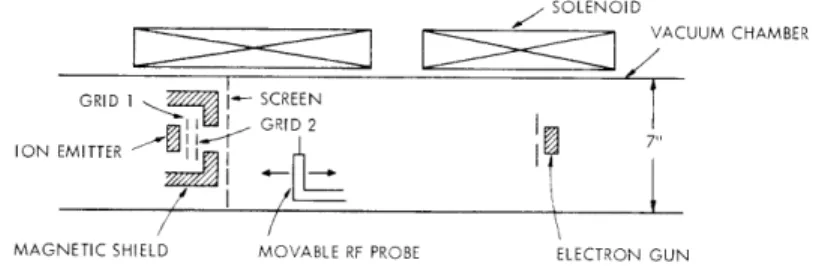
Experimental System
A schematic diagram of the experimental configuration is shown in Fig. IX-1. The
4
solid ion emitter (0. 25 in.
diameter) emits 0. 1-0. 5 mA of potassium ions ; a
(IX.
APPLIED PLASMA RESEARCH)
double-grid arrangement allows independent control of the beam current and energy.
Because of the finite lifetime of the emitters, they were operated in a pulsed mode,
typ-ically 1-ms pulses at a 5-10 pps rate. The emitter voltage could be modulated by an
RF generator at frequencies in the 1-mHz range. This modulation produces primarily
a velocity modulation in the emitted beam rather than current modulation, since the
accelerating voltage from emitter to grid 1 is sufficient to saturate the emission.
SOLENOID
O E I VACUUM CHAMBER
GRID 1 j SCREEN
ION EMITTER GRID
MAGNETIC SHIELD MOVABLE RF PROBE ELECTRON GUN
Fig. IX-1. Schematic of experimental configuration.
The mirror shape of the magnetic field was produced by two pole pieces (not shown), and the ion emitter was located inside a magnetic shield to reduce electron back-streaming from the plasma. In the experiments described here, the plasma was pro-duced by an electron gun located on the opposite end of the system from the ion gun (see Fig. IX-1). The electron gun was DC operated and the distance between the guns was approximately 30 in.
Beam Modulation Studies
The initial experiments were concentrated on the technique of beam modulation and measurement of the resulting space-charge waves in the absence of plasma effects. An axially movable probe (40 mil diameter, 1/8 in. long) was used to detect the
mod-ulation on the beam; this signal was added with a reference signal and detected by a receiver to give a phase sensitive detection with linear response. The signal as a function of axial position was displayed on an x-y recorder by connecting the probe to a potentiometer that drove the x axis of the recorder.
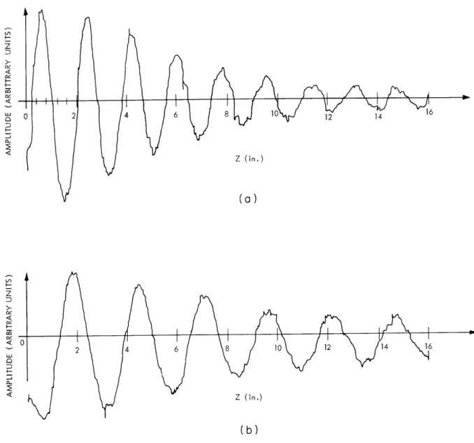
An example of the waveforms measured by this technique is shown in Fig. IX-2. The
-6
electron gun was off, and the pressure was less than 10 Torr. The decay of the wave pattern away from the ion gun (located -1 in. to the left of z = 0) is due primarily to the divergence of the ion beam because of radial space-charge forces. (The peak netic field in the system is several kilogauss, and this is insufficient to provide mag-netic focusing of the ions except at very low emission currents.) For example, the ion
4 2 4 6 1ok0 12 16 z (in.) (a) z (in.)
(b)
Fig. IX-2. Ion beam modulation vs axial distance in vacuum for a beam voltage of 500 V (a) and 1 kV (b). The emitter modulation amplitude was 5 V peak-to-peak at a fre-quency of 1 mHz, and emission current z100
pA.
(IX.
APPLIED PLASMA RESEARCH)
beam current density as a function of axial position as measured with the sliding probe
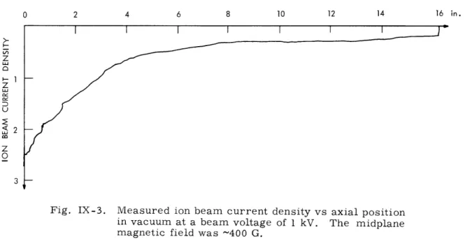
at I-kV beam voltage is shown in Fig. IX-3. Note that the decrease in current density
with z considerably exceeds the reduction in wave amplitude.
O 2 4 6 8 10 12 14 16 in. V) 0 -U o 0 3
Fig. IX-3.
Measured ion beam current density vs axial position
in vacuum at a beam voltage of 1 kV. The midplane
magnetic field was -400 G.
The wavelength of the traveling waves corresponds quite closely to the expected
value; namely, Xe =
v o/f, where v =2.2 X10 5
cm/sec is the speed of the potassium
ions.
Measurements of the wavelength at several voltages showed the dependence X
~
4
,
as expected. The measured values of wavelength are 4. 6 cm and 6. 4 cm at 500 V
and 1 kV, respectively; while the theoretical values are 4. 9 cm and 6. 9 cm. The slight
reduction in velocity observed experimentally is probably due to the space-charge
depression of potentials; in earlier experiments an even greater reduction in axial
wavelength (velocity) was observed at higher emission currents. A time-of-flight
measurement of the leading edge of the current waveform showed a similar reduction
in velocity for the same emission currents used in obtaining the data of Fig. IX-2.
The attenuation of ion beam current density with z could be overcome to a large
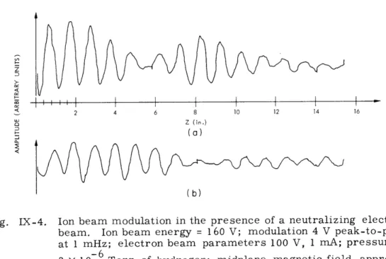
extent by providing some neutralization of the ion space charge with the electron beam.
Data showing the waveforms obtained with a 160-V ion beam in the presence of a 100-V,
1-mA electron beam at a pressure of 2
X 10
- 6Torr are shown in Fig. IX-4. These data
indicate a sinusoidal interference between the fast and slow space charge waves,
5with a "beat wavelength" (X
q)
of
~12
in. for an ion beam current of 200
p-A.
This
wavelength is the correct order of magnitude for an ion beam space-charge wavelength;
note also that the beat wavelength is longer for the lower current case, as would be
expected.
These data indicate that relatively undamped space-charge waves can
propa-gate on the ion beam when the radial beam blow-up caused by space charge is
elim-inated.
z
2 4 6 8 10 12 14 16 0 Z (in.) - (a) (b)Fig. IX-4.
Ion beam modulation in the presence of a neutralizing electron
beam.
Ion beam energy = 160 V; modulation 4 V peak-to-peak
at 1 mHz; electron beam parameters 100 V, 1 mA; pressure =
-6
2 X 10
Torr of hydrogen; midplane magnetic field
approxi-mately 250 G.
(a) Ion current ~200
p.A.
(b) Ion current -100
p.A.
Our studies of the effects of an electron beam-plasma discharge on the ion beam
space-charge waves were hampered by considerable noise from the beam-plasma
dis-charge.
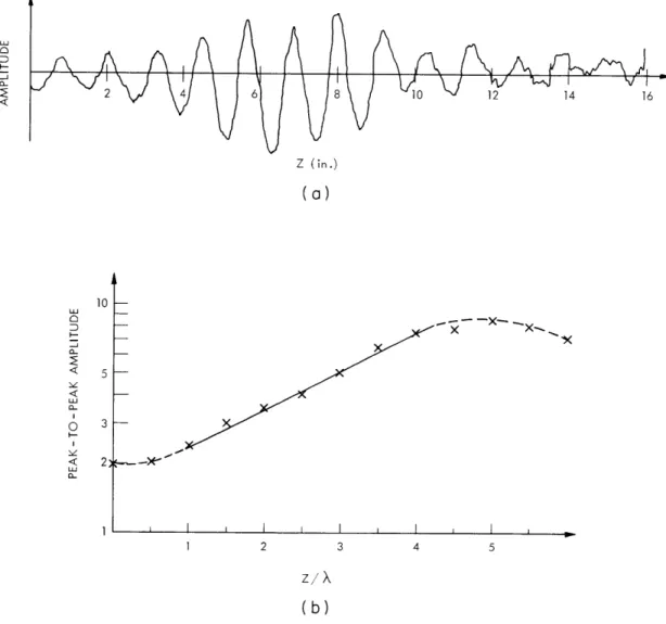
Indications of growing wave behavior have been obtained for several discharge
conditions; an example is shown in Fig. IX-5a.
A very weak discharge was created by
-4a 150-V electron beam (3
mA)
at a pressure of 1. 5
X
10-4 Torr and a midplane
mag-netic field of ~500 G.
An ion beam voltage of -225 V maximized the signal several
inches from the ion gun, and the amplitude plot on semi-log paper shown in Fig. IX-5b
indicates an exponential growth for 6-8 in. before some form of "saturation" occurred.
(Note that with growing and decaying waves present, one would not expect pure
exponen-tial behavior near z
=
0.)
The saturation did not appear to be a nonlinear effect, as
changing the modulation amplitude had little effect on it. A dependence of the
"satura-tion distance" on both the magnetic field amplitude and the beam voltage has been
observed.
Data on the wave patterns in the absence of a discharge over a variety
f\A A,/f\
A
1
A,
[
,A
\
z (in.)(a)
c--
-LL/0U12
X. -I I Iz/X
(b)
Modulation pattern in the presence of a weak beam-plasma discharge. Ion beam voltage 225 V, current 100
p.A,
modulation 20 V peak-to-peak at 1 mHz.(a) Wave pattern.
(b) Peak-to-peak amplitude vs z/k. Fig. IX-5.
n ,
i
of pressures (10- 6 < p < 10- 3 Torr Hg) do not indicate appreciable scattering of the ions -4
over these distances at pressures of 10 Torr.
The donation of the solid ion emitters by Dr. P. Chorney and Dr. S. F. Paik of Microwave Associates, and the assistance of D. S. Guttman in the early phases of the work are gratefully acknowledged.
R. J. Briggs References
1. R. J. Briggs, Electron-Stream Interaction with Plasmas (The M. I. T. Press, Cam-bridge, Mass. , 1964).
2. M. A. Lieberman, "Ion Oscillation Excited by Electron Beam-Plasma Interaction," Ph. D. Thesis, Department of Electrical Engineering, M. I. T. , June 1966.
3. R. R. Bartsch, "Investigation of Non-syrichronous Beam-Plasma Interaction," Ph. D. Thesis, Department of Electrical Engineering, M. I. T. , July 1968.
4. K. K. Chow, H. S. Maddix, and P. Choirney, Appl. Phys. Letters 10, 256 (1967). 5. W. H. Harman, Fundamentals of Electronic Motion (McGraw-Hill Book Company,
IX. APPLIED PLASMA RESEARCH
B.
Plasma Effects in Solids
Academic and Research Staff
Prof. A. Bers
Dr. L. D. Pleasance
Graduate Students
Y. S. Lau
H. Mok
R. N. Wallace
1. FURTHER STUDIES 'OF A MODEL FOR MICROWAVE EMISSION
FROM THE BULK OF n-TYPE INDIUM ANTIMONIDE
We have continued the study of the model for microwave emission from n-type indium
antimonide which was presented in our previous report.
This model was developed to
explain experimental results
2obtained with round loop samples subjected to DC
mag-netic and induced RF electric fields. A number of corrections and additions to the
orig-inal model have now been made.
The basic conclusions of the previous report
remain unchanged, however.
The observed microwave emission is identified as shot
noise produced in localized inhomogeneities in the sample material when electrons gain
energy in crossed electric and magnetic fields and undergo ionizing collisions.
Variation of Emission Level with Sample Rotation
For a round loop-sample mounted in the cross-sectional plane of an eccentric
trans-mission line,
3the microwave power delivered to the receiver is given by
42
1
o
A
-S =
eJ
dA
,
(1)
2 A
where po and E are the permeability and permittivity of the medium (liquid nitrogen)
filling the transmission line, J is the microwave current distribution on the sample,
A 5
e is the normalized
electric field mode function for the TEM mode in the eccentric
transmission line, and A is the cross-sectional area of the line.
(In the previous
A - A
report, the magnetic field mode function h X i should have been used instead of h.)
zFor comparison with experiment, it was assumed that a single localized microwave
current source was present on the loop sample.
The current distribution J on the
sample was computed, and the expression (1) was evaluated as a function of sample
rotation. Results were normalized to unity at the position of maximum output, and plotted along with similarly normalized experimental results obtained for loop samples subjected to crossed electric and magnetic fields of constant amplitude. A typical result is shown in Fig. IX-6. The agreement between theory and experiment is quite good.
ECCENTRIC TRANSMISSION LINE
S- I
odo
2 LI w 0 oI.c w 0 0.5 w I-> ._J LU XFig. IX-6.
--- EXPERIMENT - THEORY /I/ \/I 0 45 90 135 180 225 270 315 360 ANGULAR ROTATION, DEGREESComparison of the observed variations of microwave emission level as a function of angular rotation of the sample with computations, under the assumption of the presence of a single localized current source. Exper-imental conditions: Sample6 R-8; E = 54 V/cm; B = 5. 1 kG; f = 9. O GHz.
0
The "single source" model predicts two maxima in emission level separated by
per-fect nulls.
The nulls are always 1800 apart, and the patterns are symmetric about the
positions of the nulls.
However, the maxima are not exactly
1800
apart; indeed, because
of the changes in the microwave current distribution
I
at different frequencies, the
maxima appear closer together at 3 GHz than at 9 GHz.
A comparison between theory
and experiment at both 3 GHz and 9 GHz is shown in Fig. IX-7. Again, the agreement
(IX. APPLIED PLASMA RESEARCH)
between theory and experiment is reasonably good. The data presented here for samples
R-1 and R-86 suggest that a single microwave source was dominant in each sample. We do not assert that all samples which produced emission contained one and only one
SAMPLE R-I THEORY --.- EXPERIMENT 1.0 9GHz 0.5 L / \ Fig. IX-7.
0o Comparison of the "single-source"
-' / - model with experimental results at
> 0 3 GHz and 9 GHz. Experimental conditions: E =54 V/cm; B a0 5. 1 kG.
J
\3GHz
" 0.5 0 I \I 0 0 90 180 270 360ANGULAR ROTATION, DEGREES
source. In particular, some samples7 produced poorly-defined patterns of maxima and minima when rotated. This is taken as an indication of the presence of multiple sources. Matching of Experimental Threshold Fields and Microwave Power
Level with the Shot-Noise Model
The method for fitting the threshold electric and magnetic fields and the microwave power level observed experimentally to the shot noise model was treated in some detail in our previous report.1 Near threshold, it is assumed that one localized microwave source (i. e. , the strongest source) produces most of the emission from a particular
sample. The source is conjectured to be a thin (1-10 p) region where the electric field is 2-4 times larger than the applied electric field. In the high field region, a fraction F of the electrons gains sufficient energy to cause ionizing collisions, producing a shot-noise current of rms value (2eFI Af)1/2, where Af is the receiver bandwidth and I is the
sample drift current. This current is then the magnitude of the "localized" current source used for the computation of the microwave current distribution J on the sample. Once J is known, the microwave power delivered to the receiver can be computed from Eq. 1. Along the threshold E -B curve, the microwave power is constant and roughly equal to the emission which would be observed from a thermal source at a temperature
of
10
3 oK.To maintain the constant threshold power level in the theoretical model, the
product FIl must be a constant. The fraction F depends on the assumed magnitude and variation of the electric field E. in the localized high-field region and on the electron distribution function f. When definite assumptions about f and E. have been made, F is determined as a function of E and B . The drift current I is known as a function
o0 0 2 o
of E and B from magneto-resistance measurements. Thus the product FI can be
determined as a function of E and B , and the loci FI = constant in the E -B plane
are the theoretical threshold curves.
It is well known that in InSb polar optical mode scattering plays an important role in characterizing the high energy part of the electron distribution function, while the low energy part is mainly affected by acoustic mode scattering. At present there exists no satisfactory theory for the electron-distribution function in our range of applied fields. For fitting our experimental data of the threshold E -B fields and the threshold noise power we need to know the distribution function only in so far as it determines
#H
1
and the number of electrons above the energy Ca which will produce ionizations. In our
-1 2
previous report we assumed H ~ E-i and a distribution function with T ~ E in the
low-energy range and Te - E in the high-energy range. This together with the assump-tion of a constant field enhancement factor M z 2-4, was found to fit the experimental
-1
2
data. The variation H E and T E. were erroneously assigned as following from
8H
i
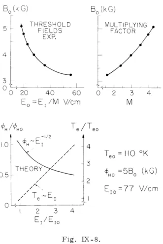
ethe theory of Budd which considers only acoustic scattering. In fact Budd's calcula-tions in the regime of our applied fields predict that the isotropic part of the distribu-tion funcdistribu-tion is Maxwellian with Te E. and consequently H -E1/
Figure IX-8 shows a fit of the experimental data using Budd's model for the distri-bution function. A single-temperature Maxwellian distribution was used to describe the entire electron population. The initial value PHo for the tangent of the Hall angle was determined from a typical value of the low-field electron mobility in n-InSb. The
initial values E. and T were chosen to place values of €a9 in an energy range where
10 eo a 1
previous computations of electron energy gain were valid. When the multiplying factor M = Ei/Eo was allowed to vary as shown with B o, the threshold fields and micro-wave power level were matched exactly. We note, however, from Fig. IX-8 that Ei
and Te actually vary only slightly over the length of the threshold curve. Since (E) B >> 1 for most electrons P ~ H M2E2 and one may alternatively fix M at a
con--1 1
stant value, and allow H to vary as Eo as in our previous report. In this case there is no known solution for the distribution function which would give us such a variation
(IX.
APPLIED PLASMA RESEARCH)
of H. However, with appropriate choices of M and the initial electron temperature, this model compares favorably with the observed threshold characteristic, as shown in Fig. IX-9. Here a single temperature (with T - E ) Maxwellian distribution was
used to describe the entire electron population. used to describe the entire electron population.
Bo (k G)
THRESHOLD 5 FIELDS EX P. 4 3 0 20 40 60E
o=E /M
V/cm
Bo (k G)
MULTIPLYING FACTOR/
0 2 3 4M
9GHz THRESHOLD CHARACTERISTIC 5.5 U 5.0 -4.5 Bo(kG) 4.0 3.5 3.0 0 H / HOTe/Teo
-1/2 IO 'I4
THEORY /2 ,I
I 2 3 4EI/EI0
Teo =
110
OK
HO =5Bo(kG)
EI
0=77
V/cm
#H /OHO ---- EXPERIMENT THEORETICAL MODEL To= 960K \ Ho=5Bo (kG) M=4.4 ).5 2 T o 00 20 30 40 50 60 70 Eo(V/cm) Fig. IX-8.A fit of the experimental threshold fields
using Budd's calculations of the distribu-tion funcdistribu-tion. When Te' H' and M vary as indicated, an exact fit to the experi-mental threshold fields and microwave power level is obtained.
Fig. IX-9.
A fit of the experimental threshold
data with the assumptions of
con--1
stant MiI, T ~ Eo and H ~EO
e o
These models can also be used to predict the variation of the observed emission level
for fields above threshold once they have been matched to the measured threshold
char-acteristics.
Both models predict that the emission level increases more rapidly with
increasing field than is observed experimentally.
The model based on Budd's theory
gives somewhat poorer fits to the typical experimental results.
A more detailed test of our shot noise model for microwave emission from indium
Te/Toantimonide requires a knowledge of the electric field in the inhomogeneity and of the electron energy distribution in moderate electric and magnetic fields. From the present model the locations of the inhomogeneities responsible for the emission can be deter-mined, and direct electricall0 or photo-conductivell probes may reveal the field dis-tribution in the inhomogeneities. Further, the methods used recently 2 to study hot electrons in GaAs might be applied to InSb. Thus, methods for testing the shot-noise model appear to be available and could be applied in future studies.
R. N. Wallace, A. Bers
References
1. A. Bers and R. N. Wallace, Quarterly Progress Report No. 97, Research Labora-tory of Electronics, M. I. T. , April 15, 1970, p. 77.
2. R. N. Wallace, Quarterly Progress Report No. 96, Research Laboratory of Elec-tronics, M.I.T., January 15, 1970, p. 131.
3. R. N. Wallace, ibid. , Fig. XX-7, p. 133.
4. In deriving this form, it was assumed that the sliding short behind the sample was tuned for maximum signal.
A A
5. A e e dA = 1.
6. R. N. Wallace, Quarterly Progress Report No. 96, op. cit. , Table XX-1, p. 132. 7. R. N. Wallace, ibid. , Fig. XX-16, p. 142.
8. H. F. Budd, Phys. Rev. 131, 1520 (1963).
9. A. Bers and R. N. Wallace, op. cit. , Fig. IX-9, p. 80.
10. A. H. Thompson and G. S. Kino, I. B. M. J. Res. Develop. 13, 616 (1969). 11. D. L. Spears and R. Bray, J. Appl. Phys. 39, 5093 (1968).
12. A. Mooradian and A. L. McWhorter, Proc. 10th International Conference on the Physics of Semiconductors, Cambridge, Mass. , 1970 (to be published).
(IX. APPLIED PLASMA RESEARCH)
2.
ELECTRON PLASMA SURFACE WAVE IN CROSSED
ELECTRIC AND MAGNETIC FIELDS
We shall show that the free electrons in an n-type semiconductor can propagate weakly damped surface waves. The geometry under consideration and the relative
directions of the applied fields are sketched in Fig. IX-10. The nature of these waves is quasi-electrostatic, with electron bunching near the surface and heliconlike electron motion away from the surface. Depending upon field orientations, these waves may have either positive or negative small-signal energy. Hence they can be used for coupling and amplifying signals. We shall summarize the theoretical model descriptions of these waves in this report. We assign to the electrons an effective mass and constant relax-ation time, and assume that they are uniformly distributed throughout the material. We
SEMICONDUCTOR y
n-TYPE
///////////////////// x
z
Fig. IX-10.
Geometry of semiconductor surface
Eo and applied fields.
Bo
restrict ourselves to frequencies that are small compared with the electron-lattice col-lision frequency, and wavelengths that are long compared with the electrons' mean-free path.
Theoretical Model with Diffusion Effects Ignored
The description of surface waves on an anisotropic plasma is well known. For a quasi-electrostatic surface wave in which the electron bunching is finite only at the
surface (the interface between media 1 and 2), the field variations are of the form exp j(wt-zq) - q y , and the dispersion relation is
E1(l , q) = -E 2(w, q), (1)
where E(w, q) is the dielectric response function for the electric displacement normal to the surface. In the case of Fig. IX-10, with vacuum above the semiconductor, we
obtain
E sK
,
r( q) = -E (2)where K and Kr are the relative dielectric functions for the left- and right-hand circu-lar pocircu-larization of the fields about B .o Hence it suffices to consider in detail only
one of the two dispersion relations of Eq. 2; the other may reversing the magnetic field. For the field orientations in Fig.
E S
be derived from it by
IX-10 we then find
w
(b-j)+ -E
(w-qv00
c - qv = -M '(b-j), (4)
where vo = -[,E is the electron drift velocity, b= Bo 0 c/v is the ratio of the electron-cyclotron frequency to the electro-lattice collision frequency, o = - / is the
dielec-2 -1
tric relaxation frequency of the material, w w a/(1+b ), and M = (1+/E s
0
b b
~~-~1-~~~
Fig. IX- 11. Dispersion characteristics [(a), b > 0; (b), b < 0]
for the electron surface wave under the assumption of negligible effects attributable to diffusion.
b -= /M (b, Qb- Eq v /MW -b.
Consider these waves as a function of real excitation frequencies o. From Eq. 4
we have
Me
- + b (5)
r v v
(IX. APPLIED PLASMA RESEARCH) and q. -1/b q r " r + 1 MwI b (6)
0-Equation 5 is sketched in Fig. IX-11 for both b > 0 and b < 0. In the absence of an applied magnetic field, b = 0 and weakly damped waves exist only for w >> M 0 . This condition requires very low electron densities and hence strongly limits the choice of materials. In the presence of a magnetic field weakly damped waves can exist for almost all frequencies (except in the vicinity where qr = 0) provided b > 1, as is shown
in Fig. IX-11.
Energy Characteristics of the Waves
For the weakly damped waves we can calculate the time-averaged energy per unit length in the direction of propagation. Following well-known results, 2
we obtain for quasi-electrostatic surface waves
0 1 2 1c
I(w'q)
0 c , q)(W) = -00 dy E1 8 , + dy 4E 2
a
0q
(7)40 4
Using the fact that E = -V) and the y-dependence of the fields exp -q y , we find for the waves of interest
h
8K, r q)
(
W)
-q
s
i(q)'
(8)
where a is the amplitude of the potential at the surface (y=0), and Kh
,r is the Hermitian
part of Kf, r' Using Eqs. 2 and 3, we find that for the weakly damped waves of Fig. IX-11la (W) < 0, while for those of Fig. IX-lib (W) > 0, as indicated. The negative energy wave can be used to amplify acoustic surface waves in a piezoelectric adjacent to the
semiconductor, or acoustic surface waves in the same semiconductor if it is piezo-electrically active. The presence of free holes near the surface can lead to two-stream or resistive-medium instabilities by interaction with the negative energy-electron surface wave. Such instabilities have been predicted' 4
5 and observed.6 Finally, the positive energy wave can be used for resonantly coupling (acoustic or electric) signals to the electrons in the semiconductor.3
Theoretical Model Including Diffusion Effects
We now consider the effects of thermal motion of the electrons. Within the hydro-dynamic model, the electrons are now also characterized by a diffusion constant
D = - KT/e = KT/mv, where K is Boltzmann's constant, and T is the electron tempera-ture.
The small-signal equations for electrons are
D Vl + -n = -(-V 1 +v lXB0 ) (9) O
an
+ V
J
= 0
(10)
at 1 -en71
(11) sThis set of equations allows independent solutions,
n1 = 0 (12a) 2f
V
= 0 (12b) andan
Sn1 * * 2 --- + onl - DVn
= 0 2 -enl E 1 n s s (13a) (13b)where we have used Eqs. 9-11 in a coordinate system moving with the electron drift
2
velocity, and D =D/l+b .For solutions of the form exp j(ct-qz), with (y< 0) df ~ exp ay and 1 n exp py inside the semiconductor, and(y> 0) o~ exp -ay outside the semicon-ductor, the free-dispersion relations for surface waves are
2 2 IReq>0, a - q = 0; Re q <0, a=q a = -q and : * 2 2 o+o o- -D (p -q ) = 0; Re p >0. (15)
(14)
(In the laboratory coordinate system o in Eq. 15 is replaced by w
-
qv ) The boundary
conditions at the surface are taken as: (a) continuity of tangential E-field; (b) continuity
(IX. APPLIED PLASMA RESEARCH)
or normal D-field; and (c) zero current normal to the surface. Imposing these boundary conditions, we obtain the dispersion relation for Re q > 0
S- qv j(w-qv ) + jb(w-qv 2
07
±
M±0
, (16)Mo(b-j) q D
L
Mw(b-j)where M' = Eo/E = -1 + 1/M. The dispersion relation for Re q < 0 is determined from Eq. 15 by replacing b with -b.
Equation 16 is of fourth order in q. The "synchronous root" j(w-qv ) + W = 0, for
0
a-which the fields vanish, can be factored out, however, and we obtain
2
2
2
- qv - q D (w-qv)(1-jb)
+ Mo',, = M ' , * (17)
S TMw (b-j)
L
M (b-j)where 'D-(D/ )1/ is the Debye length. For D= 0, Eq. 17 reduces to Eq.4. In the limit
qfD << 1 the right-hand side of Eq. 17 can be treated as a correction to the dispersion relation of Eq. 4, and we find approximately
- qv
=
-Mw (b-j) 1 ± qfD Mj
(18)Hence, in the limit of qfD << 1 a weakly damped surface wave is obtained when b >> 1 and (qfD) 2 b << 2M; that is, 1 << b << 2M/(qD) 2. Computations of the dispersion relation
are presented in Sec. IX-B. 3.
A. Bers
References
1. W. P. Allis, S. J. Buchsbaum, and A. Bers, Waves in Anisotropic Plasmas (The
M.I.T. Press, Cambridge, Mass., 1963), pp. 231, 243, and 248-252. 2. Ibid. , see Sec. 8-6.
3. A. Bers and B. E. Burke, Appl. Phys. Letters 16, 300 (1970); 17, 47 (1970). 4. G. S. Kino, Appl. Phys. Letters 12, 312 (1968).
5. R. Hirota, J. Phys Soc. Japan 23, 798 (1967).
3.
DISPERSION CHARACTERISTICS OF THE ELECTRON
PLASMA SURFACE WAVE
The dispersion relation for electron surface waves in crossed electric and magnetic fields has been found (see Sec. IX-B. 2) to be
F
(w-qv ) +
jbqv
2w
-
L
+ q D+
M.Li b) ( 1 )+ + 2 1 MW (b-3)
Mw (T(b-j)
q D
Equation 1 may be written in terms of dimensionless parameters in the form
jA 2Q (+jb)(F-G) F2 + 2 = 0, (2) 1+b where Mvi(l+jb)
F=W-Q-j
1+2
1 +b2is the cold-plasma dispersion relation, M'(l+jb) M G = jb(W-Q)- j 2 1 +b
qvo
ZDwa-
nKT
W = -, Q = , and A- 2- n vo s oThe order of Eq. 1 has been reduced from quartic in q to cubic in q by factoring out
j
the "synchronous root" w - qv° - 2. The effects of diffusion are contained in the
l+b 2
second term of Eq. 2, and are characterized by the single parameter A proportional
2
to the temperature. In the limit A - 0 the cold-plasma dispersion relation, F = 0, is recovered. The root found in this limit is degenerate, and for finite values of A2 two of the three roots of Eq. 2 will correspond to deviations from the cold-plasma solution, while the third will represent a new wave arising from the inclusion of diffusion in the theory.
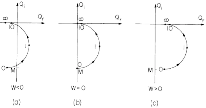
Analysis of Eq. 1 need only be considered for two applied field orientations. Solu-tions for other orientaSolu-tions may be generated by symmetry arguments. A convenient set of orientations is shown in Fig. IX-12. The direction of the drift velocity is taken
- Qr<O Qr>O
-
0--bsO
(b)
Fig. IX-12. Field orientations for the electron surface wave.
W<O W=
o Ur
W>O
Fig. IX-13. Root locus as a function of b for a cold plasma (A2 =0).
W=O W>O
Fig. IX-14. Root locus as a function of b and A2
for two of the roots of the warm-plasma dispersion relation. The surface-wave branch is shown as a solid line.
- Qr<O Qr>O q q B vo b>O
(a)
Qr 2 //Tv
0 W<O(a)
0.5 1.0
ELECTRON SURFACE WAVE
B vo
b=10
M= 0923
5 10
ELECTRON SURFACE WAVE
77Tm7777" b=1
M=0.923
ELECTRON SURFACE WAVE
0-b=0
M=0.923
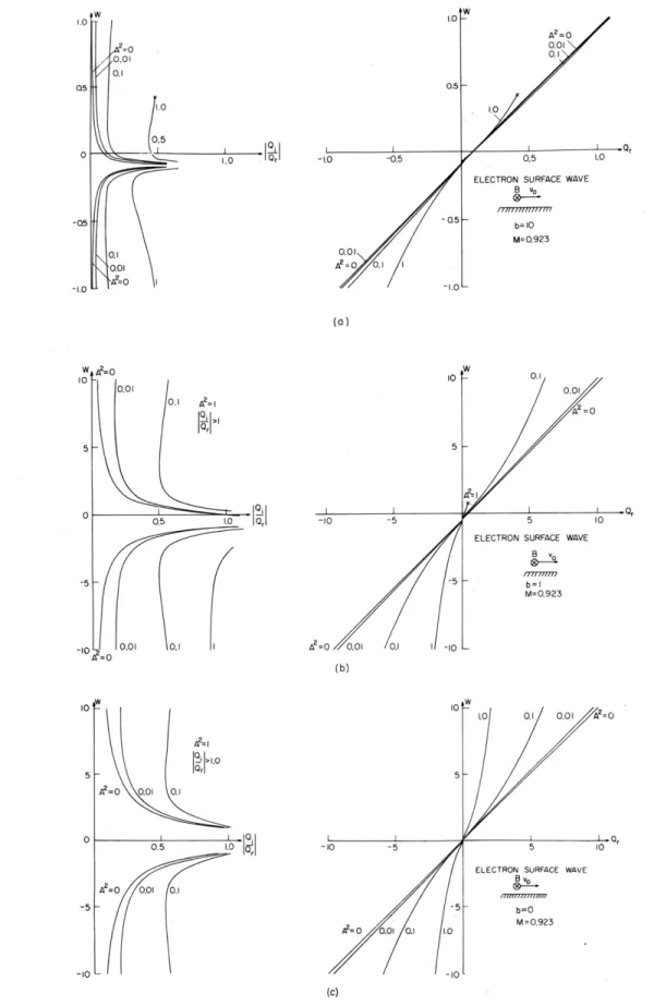
Fig. IX-15.
QPR No. 99
Dispersion relations for the electron surface wave including
diffusion. The relative damping along each of the curves is
shown at the left. Note change of scale for b
=
10.
103
(IX.
APPLIED PLASMA RESEARCH)
to be fixed. The magnetic field may be oriented in two ways with respect to the drift velocity as shown. With the use of this set, roots of Eq. 2 with positive and negative real parts correspond to propagation parallel and antiparallel to the drift velocity, respectively. If negative frequencies are included, solutions need only be calculated for one of the two cases shown in Fig. IX-12, since they are related by the trans-formation (b -- b, W -- W, Q--Q ).
Some general characteristics of the roots of Eq. 2 may be obtained by examining their locus on the complex Q-plane as a function of b as shown in Fig. IX-13. With increasing frequency the root locus is drawn monotonically to the right as shown. The wave is weakly damped for sufficiently large positive or negative frequencies and for b >> 1. For a finite A2 the single-root locus for a cold plasma splits into two branches as shown in Fig. IX-14. As before, increasing frequency moves the loci to the right. With increasing A the separation from the cold wave increases and the roots move toward the origin as shown.
Each of the roots of the dispersion relation must be tested to determine whether the associated fields decay away from the surface, as required of a surface wave. Cutoffs will occur when either of the two waves required to satisfy the boundary conditions at the surface fail this test. Only the branch drawn in solid lines in Fig. IX-14 is a true surface wave. Each branch is cut off as it crosses the imaginary axis, and the surface wave shifts from one branch to the other. Furthermore, at some positive frequency the surface wave will cease to exist because of the cutoff of the thermal component of the surface wave.
0i
W>O
>0Fig.
IX-16. Root locus of the third root of the
warm-plasma dispersion relation. This root isb / a surface wave only for Q > 0 as shown
\a2
by the dashed line.
The dispersion relation for the electron surface wave is plotted in Fig. IX-15 for several values of b and A . The corresponding value of lqi/qr I along each curve is shown at the left. Only qi/qr < 1. 0 are shown, since higher values represent waves that cannot be considered weakly damped. An important effect of diffusion (A 20) is
2
2
to increase the damping of the wave. For A = nKT/E E2 << 1 the damping is
essen-2 s o
tially independent of diffusion. For finite A the curves are discontinuous for Q = 0, as the surface wave changes branches. The cutoff of the thermal component of the surface wave is apparent only in the curves for A2
![Fig. IX- 11. Dispersion characteristics [(a), b > 0; (b), b < 0]](https://thumb-eu.123doks.com/thumbv2/123doknet/14056109.460741/15.918.241.622.461.814/fig-ix-dispersion-characteristics-a-b-gt-lt.webp)