Publisher’s version / Version de l'éditeur:
Vous avez des questions? Nous pouvons vous aider. Pour communiquer directement avec un auteur, consultez la Questions? Contact the NRC Publications Archive team at
[email protected]. If you wish to email the authors directly, please see the first page of the publication for their contact information.
https://publications-cnrc.canada.ca/fra/droits
L’accès à ce site Web et l’utilisation de son contenu sont assujettis aux conditions présentées dans le site LISEZ CES CONDITIONS ATTENTIVEMENT AVANT D’UTILISER CE SITE WEB.
AIP Advances, 10, 10, pp. 1-5, 2020-10-07
READ THESE TERMS AND CONDITIONS CAREFULLY BEFORE USING THIS WEBSITE. https://nrc-publications.canada.ca/eng/copyright
NRC Publications Archive Record / Notice des Archives des publications du CNRC :
https://nrc-publications.canada.ca/eng/view/object/?id=040a986c-e28a-4b4e-965f-3adc8a8c6ff9
https://publications-cnrc.canada.ca/fra/voir/objet/?id=040a986c-e28a-4b4e-965f-3adc8a8c6ff9
This publication could be one of several versions: author’s original, accepted manuscript or the publisher’s version. / La version de cette publication peut être l’une des suivantes : la version prépublication de l’auteur, la version acceptée du manuscrit ou la version de l’éditeur.
For the publisher’s version, please access the DOI link below./ Pour consulter la version de l’éditeur, utilisez le lien DOI ci-dessous.
https://doi.org/10.1063/5.0021739
Access and use of this website and the material on it are subject to the Terms and Conditions set forth at
Consistent probe spacing in multi-probe STM experiments
Consistent probe spacing in multi-probe
STM experiments
Cite as: AIP Advances 10, 105213 (2020);doi: 10.1063/5.0021739
Submitted: 14 July 2020 • Accepted: 17 September 2020 • Published Online: 7 October 2020
Jo Onoda,1 Doug Vick,2 Mark Salomons,2 Robert Wolkow,1 and Jason Pitters2,a)
AFFILIATIONS
1Department of Physics, University of Alberta, Edmonton, Alberta T6G 2E1, Canada
2Nanotechnology Research Centre, National Research Council of Canada, Edmonton, Alberta T6G 2M9, Canada a)Author to whom correspondence should be addressed:[email protected]
ABSTRACT
Multi-probe scanning tunneling microscopy can play a role in various electrical measurements and characterization of nanoscale objects. The consistent close placement of multiple probes relies on very sharp apexes with no other interfering materials along the shank of the tip. Electrochemically etched tips can prepare very sharp apex tips; however, other asperities on the shank can cause interference and limit the close positioning of multiple tips to beyond the measured radii. Gallium focused ion beam (FIB) milling is used to remove any interfering material and allow closely spaced tips with a consistent yield. The tip apex radius is evaluated with field ion microscopy, and the probe spacing is evaluated with STM on hydrogen terminated silicon surfaces. FIB prepared tips can consistently achieve the measured probe to probe spacing distances of 25 nm–50 nm.
© 2020 Author(s). All article content, except where otherwise noted, is licensed under a Creative Commons Attribution (CC BY) license (http://creativecommons.org/licenses/by/4.0/).https://doi.org/10.1063/5.0021739., s
Multi-probe scanning tunneling microscopy (M-STM) has advanced in recent years from custom built to commercially avail-able systems as researchers strive for atom resolving multi-tip sur-face analysis with the ability to controllably contact and electri-cally probe surfaces.1–10 Several studies have shown the advan-tages of M-STM on various types of samples such as semicon-ductors,11–18graphene,19–21carbon films,22and topological insula-tors.23–26Recently, the resistivity of an atomic step on a silicon sur-face was measured,12,16and lithographically prepared dangling bond (DB) wires on a germanium surface were also measured.14,15 How-ever, one issue in measuring small structures is the ability to consis-tently prepare closely spaced probes at distances less than 100 nm. This is because the close spacing is determined not only by the apex sharpness but also by the geometry between the multiple tips and the shoulders/shanks of the probes themselves. Establishing a procedure that achieves a separation distance less than 100 nm would allow for routine measurement of transconductance experiments14,27–29of nanoscale objects.
In this paper, we describe methods used to prepare closely spaced probes in the Omicron LT Nanoprobe system. This sys-tem has four scannable probes, all with angles of ∼45○
to the surface, organized in a square arrangement. We consider various
methods to prepare closely spaced probes including electrochem-ical etching of probes, Field Ion Microscopy (FIM) imaging of probe apexes, and focused ion beam (FIB) milling of probes. We found that although electrochemical etching can occasionally cre-ate closely spaced probes, and FIM measurement confirmed very sharp apexes, protrusions on the shoulders of the tips limited the close spacing. Implementing an FIB milling routine to remove asperities/protrusions allowed for consistent close spacing of probes. There are two geometries to optimize in a four probe arrange-ment. Opposite facing probes have a 90○angle between them, while
adjacent probes are closer to 60○. For tips with perfect shanks, the
minimum separation distance is just over the sum of the radii (to avoid tunneling between tips). Figure 1shows this schematically. However, any protrusions beyond this radius can dramatically affect the separation distances as will be discussed in this paper.
Generally, STM tips are prepared using a DC electrochemical etch method.30,31In this method, a tip of smooth concave etch pro-file is prepared. In most cases during the electrochemical etch, the tips are sufficiently far from the wire edge that close placement of the probes is not an issue. This is usually true for opposing tips. How-ever, if tips are blunt or the tip apex is off-center from the central axis of the wire or there is a slight bend in the wire, it is possible that
FIG. 1. Tip geometry. (a) Schematic of two probes at 45○. R is the tip radius, and
the separation distance minimizes at R + R. The shank includes the tip surface beyond R. (b) Four probes contacting a similar surface point. Opposing tips are 90○, while adjacent probes are ∼60○.
FIG. 2. SEM images of various tips in multi-probe STM: (a) interfering shanks
of adjacent tips; (b) automatic withdrawal during etching creates long tips with minimal shank interference while also providing a good SEM view of the tip region.
adjacent tips cannot measure the same area.Figure 2(a)shows a case where the wire body restricts the probe position for adjacent probes. Because of this potential interference, the electrochemical etching system incorporated an automatic withdrawal method that slowly
withdrew the wire during the electrochemical etch.32,33This creates a longer etched region that easily allows the probes to be positioned closely. In addition, because the field of view of the apex is greater when imaged with SEM, it is easier to identify regions of interest on the surface for the probe to interact with.Figure 2(b)shows two probes etched using this method. The probe on the left (A) was con-stantly withdrawn from the solution, while the right probe (B) was withdrawn and then stopped prior to etching. The stationary period of the etch created a short concave section close to the tip apex. The typical etching parameters involved a withdrawal rate of ∼1 mm over ∼10 min (our typical DC etching time for 0.25 mm wire thickness in 2M NaOH).
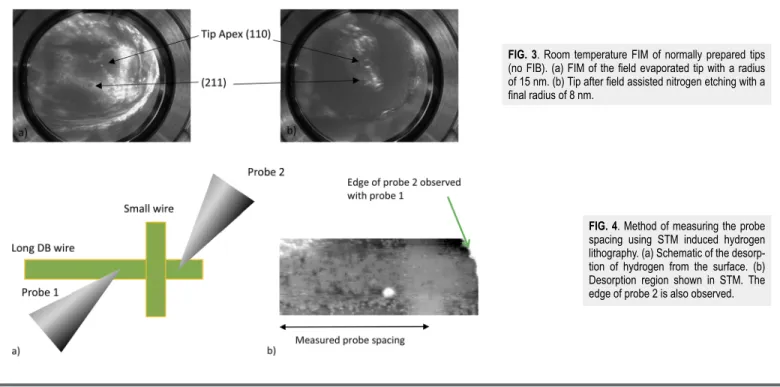
In order to evaluate the close spacing of the tunneling tips, one needs to first know the radius of curvature of the apex. This can be achieved by observing the tip apex using a field ion microscope,34 which has been integrated with various STMs in the past.35 Prior to FIM imaging, the tips were e-beam heated in order to degas and remove surface contamination and/or oxide. The field ion micro-scope was then backfilled with helium gas for imaging. Imaging of the apex atoms occurred gradually as the voltage increased, indicat-ing that the surface was generally clean from the e-beam procedure (no blow-off of oxide or dirt was observed). Field evaporation was performed to create a clean crystalline apex. The FIM images have some distortion as the apex is not orthogonal to the screen.
The radius of curvature of the tip was determined by the ring counting method34 where the number of rings between two crystallographic directions can evaluate the radius
R = ns/(1 − cos γ),
where n is the number of rings, s is the step height, and γ is the angle between crystal directions. We evaluated the number of rings between the (110) and (211) directions of the observed tips. The tip
FIG. 3. Room temperature FIM of normally prepared tips
(no FIB). (a) FIM of the field evaporated tip with a radius of 15 nm. (b) Tip after field assisted nitrogen etching with a final radius of 8 nm.
FIG. 4. Method of measuring the probe
spacing using STM induced hydrogen lithography. (a) Schematic of the desorp-tion of hydrogen from the surface. (b) Desorption region shown in STM. The edge of probe 2 is also observed.
FIG. 5. Histogram of the measured tip spacing for normal probes (no FIB
treatment).
imaged inFig. 3(a)was determined to have a radius of curvature of ∼15 nm. In some cases, the tips were further sharpened by the field controlled nitrogen etching method.36–38Figure 3(b)shows the same tip after etching, with a radius of curvature of ∼8 nm. This probe was only marginally etched in order to reduce its radius.
After determining the tip radius, the tip was transferred, in vac-uum, to the nanoprobe vacuum chamber with no air exposure. Tips were not installed into the nanoprobe unless they were deemed sharp in the field ion microscope, with a measured radius of curvature below 20 nm.
Once the probes were placed in the STM Nanoprobe, a pro-cedure to determine the minimum distance between them was required. We used STM imaging and hydrogen desorption lithogra-phy to prepare dangling bond (DB) patterns on a silicon surface that can determine the probe spacing.Figure 4shows this schematically and with STM images. The procedure implemented to determine the spacing was as follows:
(1) Probe 2 desorbed a larger patch (wire) of hydrogen, creating a long silicon DB wire.
(2) Probe 2 was then moved to the end of the desorbed wire [right side inFig. 4(a)].
(3) Probe 2 was set stationary over the end of the wire. (4) Probe 1 was then scanned until the long wire was found (on
the left side of the wire).
(5) Probe 1 was moved along the wire until contact between the two probes occurred. Probe 1’s absolute XY position is recorded.
(6) Probe 1 was removed from contact of probe 2 by a set amount of 50 nm and set stationary.
(7) Probe 2 then drew a perpendicular wire as a marker on the surface.
(8) Probe 2 was then removed from the perpendicular wire. (9) Probe 1 was repositioned by the 50 nm offset to its initial
contact position.
(10) Probe 1 then scanned an image that could observe the per-pendicular wire. The distance measured to the center of the perpendicular wire from probe 1’s absolute XY contact posi-tion was taken as the distance between the two apexes of the tips.Figure 4(b)shows the edge of probe 2 imaged with probe 1 while imaging the silicon DB wires.
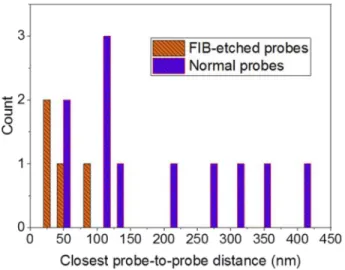
Using this procedure, the closest measured distance between two probes that were electrochemically etched and FIM evaluated was tested. Figure 5 shows the evaluated distances for multiple experiments. The closest distances between probes varied greatly, from ∼50 nm to over 400 nm, despite the field ion microscope’s radius of curvature always measured below 20 nm (Fig. 5).
This led to the conclusion that some other portion of the tip was interfering prior to the apex region. In order to deter-mine the structure of tips, SEM images were acquired in a Hitachi dual beam SEM FIB system. The tips were mounted in the SEM FIB with the same 45○ orientation as in the STM Nanoprobe.
Figure 6(a)shows an example SEM image of a probe. As shown inFig. 6(b), there is a protrusion at the shoulder location near the apex. It is believed that these protrusions limit the spacing of the probes.
FIG. 6. FIB procedure to shape the probe apex and shoulders. (a) SEM of the typical tip. (b) Close-up SEM of the tip apex. The STM imaging portion is shown for a
45○mounted tip. Protruding shoulders are also shown. The yellow box indicates the approximate milling region to cut the tip. (c) Tip after FIB shaping and polishing
along the indicated blue lines. The apex remains sharp, and the shoulders are removed to allow for close spacing. (d) FIM of the FIB prepared tip showing a sharp apex.
In order to reduce the imperfections of the probes, they were reshaped with a gallium FIB. During this process, the end of the probe was removed with a gallium beam set at 30 kV, 150 pA. The gallium beam was rastered over a region approximately indicated by the yellow box inFig. 6(b). This removed a portion of the tip. After cutting, the apex was polished using a 30 kV, 10 pA beam rastered on line segments positioned proximal to the tip apex, as indicated schematically inFig. 6(c)by blue lines. The segments were initially positioned in the vacuum and were nudged in 20 nm increments toward and into the tip material. Simultaneous SEM imaging per-mitted the milling to be monitored and terminated once a clean cut back apex was observed, as inFig. 6(c). This process was per-formed on relatively sharp initial tips. Severely blunted or damaged tips could also be repaired; in such cases, a significant amount of material must first be removed using higher current FIB probes in order to reshape the probes and create a new apex, allowing the fine polishing steps to be applied.
Once FIB machining was completed, probes were again installed in the LT Nanoprobe. FIM imaging again confirmed a sharp tungsten apex below 20 nm based on magnification [Fig. 6(d)]. Note that gallium contaminants left over at the tip apex after FIB milling were removed by field evaporation.
STM and hydrogen desorption lithography procedure (Fig. 4) were again used to determine the closest spacing between probes. The measured distance on the FIB prepared tips is shown inFig. 7. The data from the FIB probes are overlaid with those from the nor-mal probes (no FIB processing fromFig. 5). It was determined that the FIB probes could consistently achieve distances under 50 nm.
The close tip spacing in multi-probe scanning tunneling microscopy does not rely solely on the radius of curvature of the tip apex in order to determine the minimum multi-tip displace-ment. Although electrochemically etched tips can have very sharp radii, as measured by FIM (∼15 nm), the probe spacing can vary greatly from 50 nm to over 400 nm with the majority of spacings greater than 100 nm. SEM imaging shows that electrochemically
FIG. 7. Histogram of the measured tip spacing for normal probes and FIB shaped
probes. FIB prepared probes can consistently achieve spacings under 50 nm.
prepared tips can have asperities/protrusions that limit the close spacing. FIB milling removes any protrusions and cuts the shoul-ders of the tips to idealize the tip shape for close spacing. FIB tips can routinely obtain close placements under 50 nm. This procedure can help provide a consistent probe spacing for nanoscale electrical measurements.
We would like to acknowledge Martin Cloutier for technical help and graphics design. Funding was provided by the National Research Council of Canada, Alberta Innovates Technology Futures, the Natural Sciences and Engineering Research Council of Canada, and Compute Canada.
DATA AVAILABILITY
The data that support the findings of this study are available from the corresponding author upon reasonable request.
REFERENCES
1V. Cherepanov, E. Zubkov, H. Junker, S. Korte, M. Blab, P. Coenen, and
B. Voigtländer,Rev. Sci. Instrum.83(3), 033707 (2012).
2
T. Kanagawa, R. Hobara, I. Matsuda, T. Tanikawa, A. Natori, and S. Hasegawa,
Phys. Rev. Lett.91(3), 036805 (2003).
3S. B. Kjeldby, O. M. Evenstad, S. P. Cooil, and J. W. Wells,J. Phys.: Condens.
Matter29(39), 394008 (2017).
4
K. Li, C. Zhang, Y. Wu, W. Lin, X. Zheng, Y. Zhou, S. Lu, and J. Kang,Nano Lett.
18(3), 1724–1732 (2018).
5F. Lüpke, D. Cuma, S. Korte, V. Cherepanov, and B. Voigtländer,J. Phys.:
Condens. Matter30(5), 054004 (2018).
6
I. Matsuda, M. Ueno, T. Hirahara, R. Hobara, H. Morikawa, C. Liu, and S. Hasegawa,Phys. Rev. Lett.93(23), 236801 (2004).
7T. Nakayama, O. Kubo, Y. Shingaya, S. Higuchi, T. Hasegawa, C.-S. Jiang,
T. Okuda, Y. Kuwahara, K. Takami, and M. Aono,Adv. Mater.24(13), 1675–1692 (2012).
8T. Nakayama, Y. Shingaya, and M. Aono,Jpn. J. Appl. Phys., Part 1 55(11), 1102A7 (2016).
9
B. Voigtländer, V. Cherepanov, S. Korte, A. Leis, D. Cuma, S. Just, and F. Lüpke,
Rev. Sci. Instrum.89(10), 101101 (2018).
10J. Yang, D. Sordes, M. Kolmer, D. Martrou, and C. Joachim,Eur. Phys. J.: Appl.
Phys.73(1), 10702 (2016).
11
P. Jaschinsky, J. Wensorra, M. I. Lepsa, J. Mysliveˇcek, and B. Voigtländer,J. Appl. Phys.104(9), 094307 (2008).
12S. Just, M. Blab, S. Korte, V. Cherepanov, H. Soltner, and B. Voigtländer,Phys.
Rev. Lett.115(6), 066801 (2015).
13
S. Just, H. Soltner, S. Korte, V. Cherepanov, and B. Voigtländer,Phys. Rev. B
95(7), 075310 (2017).
14M. Kolmer, P. Brandimarte, J. Lis, R. Zuzak, S. Godlewski, H. Kawai, A.
Garcia-Lekue, N. Lorente, T. Frederiksen, C. Joachim, D. Sanchez-Portal, and M. Szy-monski,Nat. Commun.10(1), 1573 (2019).
15M. Kolmer, P. Olszowski, R. Zuzak, S. Godlewski, C. Joachim, and M.
Szymon-ski,J. Phys.: Condens. Matter29(44), 444004 (2017).
16
B. V. C. Martins, M. Smeu, L. Livadaru, H. Guo, and R. A. Wolkow,Phys. Rev. Lett.112(24), 246802 (2014).
17C. M. Polley, W. R. Clarke, J. A. Miwa, M. Y. Simmons, and J. W. Wells,Appl.
Phys. Lett.101(26), 262105 (2012).
18
M. Wojtaszek, J. Lis, R. Zuzak, B. Such, and M. Szymonski,Appl. Phys. Lett.
105(4), 042111 (2014).
19
J. Aprojanz, S. R. Power, P. Bampoulis, S. Roche, A.-P. Jauho, H. J. W. Zandvliet, A. A. Zakharov, and C. Tegenkamp,Nat. Commun.9(1), 4426 (2018).
20
J. Baringhaus, M. Ruan, F. Edler, A. Tejeda, M. Sicot, A. Taleb-Ibrahimi, A.-P. Li, Z. Jiang, E. H. Conrad, C. Berger, C. Tegenkamp, and W. A. de Heer,Nature
21
J. Baringhaus, M. Settnes, J. Aprojanz, S. R. Power, A.-P. Jauho, and C. Tegenkamp,Phys. Rev. Lett.116(18), 186602 (2016).
22
S. Hettler, J. Onoda, R. Wolkow, J. Pitters, and M. Malac,Ultramicroscopy196, 161–166 (2019).
23
L. Barreto, L. Kühnemund, F. Edler, C. Tegenkamp, J. Mi, M. Bremholm, B. B. Iversen, C. Frydendahl, M. Bianchi, and P. Hofmann,Nano Lett.14(7), 3755–3760 (2014).
24S. M. Hus, X. G. Zhang, G. D. Nguyen, W. Ko, A. P. Baddorf, Y. P. Chen, and
A.-P. Li,Phys. Rev. Lett.119(13), 137202 (2017).
25W. Ko, G. D. Nguyen, H. Kim, J. S. Kim, X. G. Zhang, and A.-P. Li,Phys. Rev.
Lett.121(17), 176801 (2018).
26F. Lüpke, S. Just, M. Eschbach, T. Heider, E. Mły´nczak, M. Lanius, P.
Schüffelgen, D. Rosenbach, N. von den Driesch, V. Cherepanov, G. Mussler, L. Plucinski, D. Grützmacher, C. M. Schneider, F. S. Tautz, and B. Voigtländer,
npj Quantum Mater.3(1), 46 (2018).
27
J. M. Byers and M. E. Flatté,Phys. Rev. Lett.74(2), 306–309 (1995).
28Q. Niu, M. C. Chang, and C. K. Shih, Phys. Rev. B 51(8), 5502–5505
(1995).
29
M. Settnes, S. R. Power, D. H. Petersen, and A.-P. Jauho,Phys. Rev. Lett.112(9), 096801 (2014).
30
J. P. Ibe, P. P. Bey, Jr., S. L. Brandow, R. A. Brizzolara, N. A. Burnham, D. P. DiLella, K. P. Lee, C. R. K. Marrian, and R. J. Colton,J. Vac. Sci. Technol., A
8, 3570 (1990).
31Y. Nakamura, Y. Mera, and K. Maeda,Rev. Sci. Instrum.
70(8), 3373–3376 (1999).
32
Y. Khan, H. Al-Falih, Y. Zhang, T. K. Ng, and B. S. Ooi,Rev. Sci. Instrum.83(6), 063708 (2012).
33
B. Zhang and E. Wang,Electrochim. Acta39(1), 103–106 (1994).
34
E. W. Muller and T. T. Tsong,Field Ion Microscopy (American Elsevier Publish-ing Company, Inc., New York, 1969).
35T. Sakurai, T. Hashizume, and S.-i. Hyodo,Prog. Theor. Phys. Suppl. 106, 387– 395 (1991).
36
R. Urban, R. A. Wolkow, and J. L. Pitters,Ultramicroscopy122, 60–64 (2012).
37
J. L. Pitters, R. Urban, C. Vesa, and R. A. Wolkow,Ultramicroscopy131, 56–60 (2013).
38M. Rezeq, J. Pitters, and R. Wolkow,J. Chem. Phys.