Patric A. Grubera)
Universität Stuttgart, Institute of Physical Metallurgy, D-70569 Stuttgart, Germany
Sven Olliges
Laboratory for Nanometallurgy, Department of Materials, Eidgenössische Technische Hochschule (ETH) Zürich, 8093 Zurich, Switzerland
Eduard Arzt
Universität Stuttgart, Institute of Physical Metallurgy, D-70569 Stuttgart, Germany; Max Planck Institute for Metals Research, D-70569 Stuttgart, Germany; and Leibniz Institute for New Materials (INM), D-66123 Saarbrücken, Germany
Ralph Spolenakb)
Laboratory for Nanometallurgy, Department of Materials, ETH Zurich, 8093 Zurich, Switzerland (Received 10 February 2008; accepted 16 May 2008)
Temperature and film thickness are expected to have an influence on the mechanical properties of thin films. However, mechanical testing of ultrathin metallic films at elevated temperatures is difficult, and few experiments have been conducted to date. Here, we present a systematic study of the mechanical properties of 80–500-nm-thick polycrystalline Au films with and without SiNxpassivation layers in the temperature range from 123 to 473 K. The films were tested by a novel synchrotron-based tensile testing technique. Pure Au films showed strong temperature dependence above 373 K, which may be explained by diffusional creep. In contrast, passivated samples appeared to deform by thermally activated dislocation glide. The observed activation energies for both mechanisms are considerably lower than those for the bulk material,
indicating that concomitant stress relaxation mechanisms are more pronounced in the thin film geometry.
I. INTRODUCTION
Microstructural and dimensional constraints in poly-crystalline thin films strongly influence their mechanical properties.1,2Small grain sizes and film thicknesses lead to high stresses at low temperatures due to the confine-ment of either dislocation motion3–5 or dislocation nu-cleation and interaction.6–9 However, at elevated tem-peratures increased stress relaxation by diffusional flow of matter between the free surface and the grain boundary is expected.10,11Thus, the mechanical properties of thin films should depend significantly on temperature.
The only technique routinely used to study deforma-tion of thin films at elevated temperatures is the substrate curvature technique.3 Using this technique, several au-thors have shown that stress relaxation in unpassivated
thin films on substrates can occur by diffusional defor-mation.12–16
The presence of a passivation layer on the surface of the film can inhibit diffusional flow and results in the activation of dislocation processes within the grains.13–15,17,18 Although this technique has provided valuable insight into the deformation behavior of thin films on substrates over a wide range of temperatures and requires little sample preparation, it is limited because it does not allow for independent control of temperature and stress or strain. Thus, it is not possible to obtain comparable data for the same sample at different tem-peratures.
To achieve more defined loading conditions, it would be desirable to adapt other techniques to elevated tem-peratures. In particular, displacement measurements with a resolution of a few nanometers are severely influenced by temperature changes due to thermal expansion of the experimental setup. Therefore, only few experiments at elevated temperatures are described in the literature. Among them are nanoindentation creep tests,19tensile or creep testing of freestanding films,20–22membrane reso-nance measurements,23and bulge tests.24,25 Due to dif-ficulties in data analysis, sample preparation, and experi-mental realization, the number of tested samples is small. a)
Present address: Universität Karlsruhe, Institut für Zuverläs-sigkeit von Bauteilen und Systemen, Kaiserstrasse 12, D-76131 Karlsruhe, Germany
b)
Address all correspondence to this author. e-mail: ralph.spolenak@mat.ethz.ch DOI: 10.1557/JMR.2008.0292
In recent years, our group has developed a novel syn-chrotron-based testing technique,26 by which it is pos-sible to characterize the stress evolution in metallic films thinner than 40 nm during isothermal tensile tests. In the current study, heating and cooling capabilities were in-troduced in the experimental setup to allow for measur-ing stress–strain curves in a temperature regime from 123 to 473 K. The samples consisted of polycrystalline Au film systems with and without additional SiNx -passivation layers on polyimide substrates. Au was cho-sen because it does not oxidize and thus can serve as a model system for a free surface. The influence of differ-ent surface and interface conditions on the deformation mechanisms of the Au films could be systematically in-vestigated. In this way, the flow stress of the different Au film systems could be determined as a function of film thickness and temperature. The measured flow stresses were used to estimate the activation energies for ther-mally activated dislocation glide and grain-boundary dif-fusional creep. Thus, additional information about the correlation of stress, temperature, and predominant de-formation mechanism was obtained.
II. EXPERIMENTAL
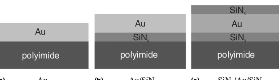
A. Sample preparation and characterization Different Au, Au/SiNx and SiNx/Au/SiNx samples were prepared (Fig. 1). The films were deposited on 125-m-thick dogbone-shaped polyimide substrates (Kapton HN, DuPont, Wilmington, DE) with a gauge section of 6 × 20 mm. Au as well as SiNx films were deposited in a direct-current (DC) magnetron sputtering system (DCA Instruments, Turku, Finland) with a base pressure of 1 × 10⁻⁸mbar. Prior to film deposition, the substrate surface was Ar+ sputter cleaned for 2 min at 200 eV and subsequently heated up to 573 K. Au films were sputtered at this temperature with an areal power density of 4.65 W/cm2, an Ar pressure of 2.5 × 10⁻³ mbar, and a deposition rate of 42 nm/min. The nominal Au film thickness was varied between 80 and 500 nm. The SiNxinterlayers and surface layers were prepared by reactive sputtering at 573 K with an areal power density of 4.65 W/cm2and an N2 pressure of 3.2 × 10
−4 mbar. The Ar flow was adjusted such that the total gas pressure was again 2.5 × 10⁻³mbar. In between Au and SiNxfilm
deposition, the gas flow was cut off, and the sputter system was pumped for 10 min. The deposition rate for the SiNxfilms was 4 nm/min, and the nominal film thick-ness was always 10 nm. Auger electron spectroscopy measurements gave an almost stoichiometric composi-tion of Si3N4. High-resolution transmission electron microscopy (TEM) images suggested that these films were nanocrystalline with a grain size of about 10 nm.
The grain size of the Au films was characterized by focused ion beam (FIB) microscopy and plan-view TEM. Films thicker than 160 nm were investigated using FIB (FEI FIB 200xP, Hillsboro, OR). To ensure the identifi-cation of all grain boundaries by the channeling contrast in the FIB, images with at least three different tilt angles between 0° and 25° were taken and compared. Plan-view TEM samples were cut out of samples with 80 and 160 nm Au film thickness and were thinned to electron trans-parency by dimpling and ion milling. TEM investigations were carried out using a 200 kV TEM (JEOL 2000FX, Tokyo, Japan). The grain boundaries from FIB and TEM pictures were drawn manually on a transparency foil and scanned to determine the area of the grains using com-mercial software (Leica Quantimet Q5501W, Wetzlar Germany). Grain size was defined as the diameter of a circle with the equivalent area and at least 400 grains were evaluated for each film. The thickness of the Au films in the different Au, Au/SiNx, and SiNx/Au/SiNx film systems was determined by Rutherford backscatter-ing spectrometry (RBS). All measurements were con-ducted using 2 MeV He+
ions (6.5MV Pelletron accel-erator of the Max Planck Institute for Metals Research). The film thickness was obtained by fitting the RBS spec-tra with the X-RUMP simulation software (Computer Graphics Service Ltd., www.genplot.com).
B. Tensile testing
X-ray diffraction measurements were performed at the MPI-MF-Beamline at the synchrotron radiation source ANKA (Angströmquelle Karlsruhe, Germany). The de-tails for the experimental procedure and data analysis of the synchrotron-based tensile testing technique are de-scribed for Au films in Ref. 26. Prior to tensile testing, the initial stress state in the films was measured by clas-sical sin2 measurements in reflection geometry. Figure
FIG. 1. Schematic drawing of the different Au, Au/SiNx, and SiNx/Au/SiNxsamples.
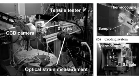
2(a) shows the experimental setup for the transmission geometry used to evaluate the stress evolution during the tensile tests. The microtensile tester (the Kammrath & Weiss, Dortmund, Germany) was mounted on the sample stage of 2 + 3 circle diffractometer. The Debye–Scherrer rings of the sample were recorded using a large area charge-coupled device (CCD; MarCCD, Evanston, IL). The elastic lattice strains in longitudinal and transverse direction were deduced from the elliptical distortion of the Debye–Scherrer rings. Subsequently, the film stress was calculated from the measured elastic strains via Hooke’s law. For calibration, tungsten powder was at-tached to the backside of the polyimide substrate by vacuum grease. The total strain of the sample was meas-ured by an optical strain measurement (2D-Strainmaster, LaVision, Göttingen, Germany).
The setup in transmission geometry enabled the deter-mination of the film stress without sample rotation and the implementation of additional devices to heat and cool the sample. The cooling system consisted of a sample chamber with two funnel-shaped openings on the back and front side for the x-ray beam and narrow slits at the top and the bottom for the sample [Fig. 2(b)]. This design prevented ice formation on the sample. The chamber was continuously filled through a flat nozzle with cold N2gas which was generated by guiding N2gas in a Cu tube coil through a reservoir of liquid N2. The temperature was controlled by adjusting the N2gas pressure and the dip-ping depth of the Cu coil in the liquid N2. Using an N2 pressure of 0.8 bar and dipping the Cu coil completely in liquid nitrogen, a sample temperature of 123 ± 5 K could be realized. For heating, a commercial heating device (Kammrath & Weiss) was mounted on the back side of the tensile tester [Fig. 2(c)]. It consists of a round ceramic heater with a central hole for the incoming x-ray beam
(2.8 mm in diameter, x-ray beamsize 1 × 1 mm). A thermocouple was positioned at the back side of the sample to measure the temperature of the sample. The thermocouple was also connected to the control unit of the tensile tester, which controlled the temperature. Ex-periments were performed at five different temperatures ranging from 123 to 473 K.
Prior to the tensile tests the evolution of thermal stresses in the Au films was characterized. A CCD frame was taken every two minutes after the heating or cooling was started until the temperature and stress in the sample remained constant. Then the tensile test was performed by increasing the crosshead displacement in steps be-tween 30 and 100m up to a maximum displacement of 1900m. Again, a CCD frame was taken for each step. The exposure time was always 30 s to ensure strain rates were nearly identical for all testing temperatures. It must be noted that no direct strain measurement was possible for the experiments at low temperatures due to the pres-ence of the sample chamber, which covered the field of view of the optical strain measurement. Therefore the crosshead displacement was calibrated by tests without a sample chamber.
III. RESULTS A. Microstructure
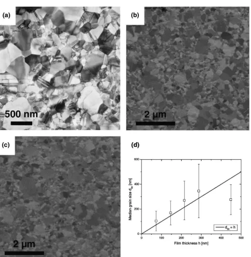
Exemplary FIB and TEM micrographs of Au and Au/ SiNx samples are shown in Fig. 3. All films had a co-lumnar grain structure with equiaxed grains in the plane of the film. Some few twins are visible in the TEM micrograph of the 80-nm-thick Au film, whereas almost no twins were found in the 160-nm-thick films. The in-troduction of a SiNx interlayer had no influence on the film microstructure, as can be seen in Figs. 3(b) and 3(c).
FIG. 2. (a) Experimental setup at the MPI-MF-Beamline for x-ray measurements in transmission geometry. The Debye–Scherrer rings of the sample and calibration were recorded on a large area CCD camera. The total strain of the sample was measured by optical means. (b) and (c) provide closer views of the cooling system and heating device, respectively. To prevent ice formation during cooling, a chamber was built around the sample. The sample temperature was measured by thermocouples.
This was also found for other film thicknesses and films with SiNx surface and interlayer. Therefore, the grain size distributions were only determined for Au samples. The grain size distributions were found to be lognormal. The median grain size values were comparable to the actual film thickness and increased linearly with increas-ing film thickness, as long as the film thickness was smaller than 300 nm [Fig. 3(d) and Table I]. For the
thickest film, the grain size stagnated. The mean values of the film thickness, measured by RBS, for different samples of the same nominal thickness are listed in Table I. The difference between nominal and real film thick-ness was about 10%. All films showed a very strong 〈111〉 fiber texture.
B. Stress–strain curves and yield strength
In Figs. 4(a) and 4(b), the evolution of temperature and thermal stresses in 160-nm-thick Au films during cooling and heating is shown. In both cases, the measured tem-perature changed faster than the stress state in the film. However, after 4 min (heating up to 423 K) or 12 min (cooling to 123 K), a constant stress level was reached. The stress state remained equibiaxial during the tempera-ture change. In principle, the thermal expansion coeffi-cient of the polyimide is higher than that of the Au film (␣PI⳱ 30 × 10 −6 K−1 >␣Au⳱ 14.2 × 10 −6 K−1 ), which should lead to compressive stresses during cooling and tensile stresses during heating. This was not observed because the samples were clamped in the tensile tester. Thus, a longitudinal contraction of the substrate during cooling was not allowed, which led to a tensile load on FIG. 3. Microstructural characterization of the different samples: TEM micrograph of (a) 80-nm-thick Au film and FIB images of (b) 160-nm-thick Au and (c) a 160-nm-160-nm-thick Au/SiNxfilm. The microstructure is not affected by the SiNxlayer; (d) median grain size versus film thickness
for Au samples. Up to 300-nm film thickness the median grain size increases linearly. Above that, the grain size stagnates.
TABLE I. Summary of microstructural data of Au samples: Nominal and measured film thickness h, median grain size d50, mean grain size
dmean, standard deviationdev, and number of detected grains N. The error for the measured film thickness is estimated from the deviation between different samples. The error of the RBS measurements was below 2%.
Sample
Film thickness h (nm)
Grain size statistics
d50 (nm) dmean (nm) dev (nm) dmax (nm) Nominal Measured N Au80 80 73 ± 3 104 126 80 653 610 Au160 160 146 ± 4 170 194 97 640 550 Au240 240 215 ± 6 269 303 155 1313 532 Au320 320 288 ± 13 346 403 215 1568 441 Au500 500 449 ± 11 276 295 121 731 541
the sample and tensile stresses in the film (the load cell showed loads of about 10 N). In contrast, the elongation of the substrate during heating was possible, which led to a distinct bending of the sample but did not affect the evolution of thermal stress in the sample. The bending of the sample had to be compensated by crosshead move-ment prior to the tensile test to ensure correct loading and straining of the sample.
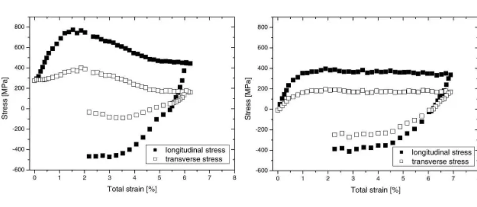
Two different types of stress–strain curves could be identified, one exhibiting a stress maximum and the other showing a stress plateau. Figure 5(a) shows the stress– strain curve of a 160-nm-thick Au film tested at 123 K. After the linear elastic regime, the film deformed plasti-cally up to a total strain of about 2%. For higher strains, the longitudinal and transverse stresses decreased con-tinuously. This stress drop is typical for stress relaxation by sequential cracking of a ductile metallic film on a compliant substrate.27,28 Upon unloading, compressive stresses developed in the film because the film was plas-tically deformed, whereas the substrate was still elastic. No delamination or buckling was observed. The comple-mentary evolution of the transverse stress was due to the mismatch in Poisson’s ratio of the Au film and the poly-imide substrate.26
The stress–strain curve of an identical
sample tested at 323 K is shown in Fig. 5(b). Here, no stress decrease was observed up to a total strain of more than 7%. Instead, stress plateaus in tension and compres-sion were found.
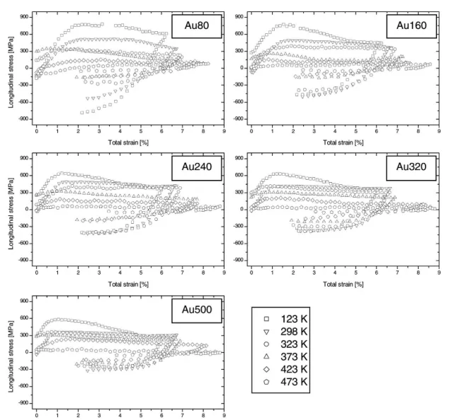
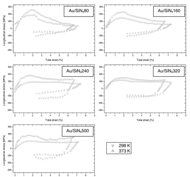
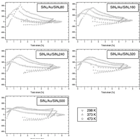
Figures 6–8 show the temperature dependence of the stress–strain curves for all film thicknesses and film sys-tems. Stress–strain curves showing a stress decrease at high total strain were observed for low and high tem-peratures as well as for samples with and without SiNx layers. For Au samples, stress drops were only found for tests at 123 K, independent of film thickness, whereas for samples with at least one SiNx layer, stress drops were obtained more likely for thinner films and all tempera-tures. The onset of the stress drop always decreased with increasing temperature. The second type of stress–strain curve without stress decrease was found for Au samples tested at intermediate temperatures and for thicker Au/ SiNxsamples. Overall, a strong temperature dependence of the stress values was found for all samples.
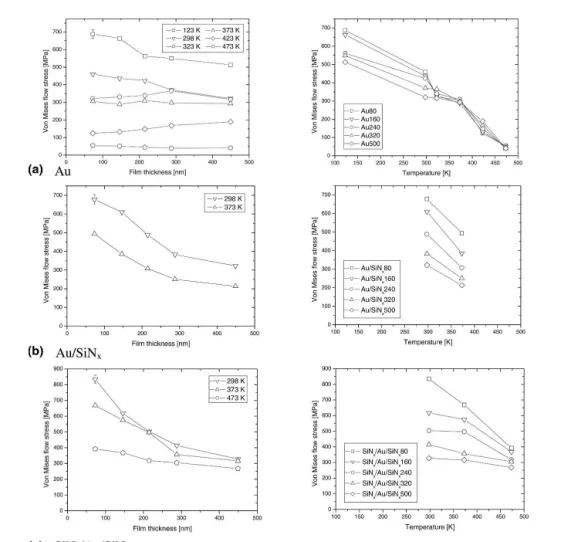
Consequently, a strong temperature dependence of the flow stresses was also observed. The flow stress was determined from the von Mises stress at 0.5% permanent strain. This was necessary to account for the biaxial stress state in the films.26
In Fig. 9, the von Mises flow FIG. 4. Stress and temperature versus time for 160-nm-thick Au films during (a) cooling down to 123 K and (b) heating up to 423 K sample temperature. The temperature of the thermocouples is plotted which differs slightly from the sample temperature. The sample temperature has been calibrated by reference measurements. An increase in equibiaxial stress is found for both cases.
FIG. 5. Stress–strain curves for 160-nm-thick Au films tested at (a) 123 K and (b) at 323 K. The longitudinal (filled symbols) as well as transverse (open symbols) is shown. The different shapes are typical for all stress–strain curves.
stress is shown as function of film thickness and temperature for all film systems. The strongest effects were found for Au samples, where the flow stress already decreased significantly for temperatures above 323 K. In addition, the thickness dependence of the flow stress dis-appeared completely. In contrast, samples with SiNx lay-ers showed much higher flow stresses for the same tem-perature or film thickness. For 473 K, the flow stress of SiNx/Au/SiNxsamples was still above 300 MPa and still increased with decreasing film thickness. The difference between Au/SiNx and SiNx/Au/SiNxsamples was low. IV. DISCUSSION
A. Low- and high-temperature fracture
The stress decrease in the stress–strain curves in Figs. 6–8 can be correlated to sequential channel cracking in the Au films. Cracking leads to local stress relaxa-tion,29,30 which results in a continuous decrease of the average film stress.27,28 Fracture was observed for Au
samples at 123 K and for Au/SiNx and SiNx/Au/SiNx samples at low and high temperatures with a decreasing fracture strain with increasing temperature. Different mechanisms may be responsible for this. The flow stress of the Au films continuously increases with decreasing temperature, indicating that dislocation plasticity is re-stricted at low temperatures, which is unusual for face-centered cubic (fcc) metals. Thus, stress concentrations around defects in the film may not be relaxed by plastic flow and lead to cracks. The situation is even more criti-cal if SiNx layers are present. Due to their brittleness, they are favorable sites of crack initiation. Once cracked, they generate additional and larger stress concentrations in the sample. This may explain why fracture was more pronounced in Au/SiNxand SiNx/Au/SiNx samples than in Au samples and could be observed at all temperatures. Lack of adhesion between the films and the substrate may be a second contributor to the fracture process.31,32 If the film is well bonded to the substrate, the substrate constraint suppresses strain localization in the film. On FIG. 6. Au samples: Stress–strain curves for 80 to 500 nm thick Au films measured at six different temperatures ranging from 123 to 473 K. For clarity only the longitudinal stress is plotted.
the other hand, if the film locally debonds from the sub-strate, it becomes freestanding and ruptures at a smaller strain than the well bonded film. The high-temperature fracture of our samples may have resulted from a weak interface between the films and the polyimide substrate. The low flow stresses at these temperatures may have enhanced necking of the films and led to the decreasing fracture strain with increasing temperature. However, a flow stress could be determined for all samples as frac-ture always occurred after the macroscopic yield point. The strong temperature dependence of flow stresses will be discussed in the following section with respect to thermally activated dislocation glide and diffusional creep.
B. Thermally activated dislocation glide
The yield strength of most polycrystalline fcc metals does not depend strongly on strain rate and temperature. Nevertheless, dislocation glide is a kinetic process, and
the strain rate ⑀˙dg for glide in the presence of discrete obstacles is given by33 ⑀˙dg⳱ ⑀˙0exp
冋
− ⌬Fdg kT冉
1− s ˆ冊
册
, (1)where ⑀˙0 is a characteristic constant taking the initial dislocation density into account;⌬Fdgthe activation en-ergy at zero stress; the applied stress; ˆ the critical shear stress, which can be interpreted as the flow stress at 0 K; k Boltzmann’s constant; T the absolute temperature; and s the Schmid factor for single crystals or strong texture.
In the following, Eq. (1) shall be used to determine ⌬Fdg as function of temperature and film thickness. Therefore ˆ is determined by extrapolating our flow stress data [Figs. 9(a)–9(c)] to 0 K and multiplying the corresponding flow stress by the Schmid factor. The strain rate⑀˙dgis replaced by the experimental strain rate of the tensile tests, which was 5.2 × 10⁻⁵s−1, s ⳱ 0.27 FIG. 7. Au/SiNxsamples: Stress–strain curves for 80 to 500-nm-thick Au films measured at 298 and 373 K. For clarity, only the longitudinal stress
(for〈111〉 fiber texture) and ⑀˙0is set to 10 −6
s−1.33Finally ⌬Fdg is calculated for the von Mises flow stress y,0.5 [Figs. 9(a)–9(c)].
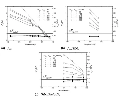
In Fig. 10, the results for ⌬Fdg are shown and com-pared to the von Mises flow stressy,0.5as well as to the activation energy⌬Fdg,bulkfor bulk Au. For Au and Au/ SiNx systems,⌬Fdg is about 1.0 to 1.3 ± 0.3 eV for all temperatures and thicknesses. This is about half of the bulk value, which is 2.01 eV.33
This may be due to the free surface in the Au and Au/SiNxfilm systems, where dislocations can leave the film leading to a lower obstacle density. In contrast, for SiNx/Au/SiNx samples, ⌬Fdg increases with film thick-ness and reaches⌬Fdg,bulkfor thicknesses above 300 nm. Here, the columnar grain structure is embedded between two stiff SiNx layers, and dislocations cannot escape from the film. This may lead to a pileup of dislocations at the interfaces and an increasing back-stress on other dislocations.8The fact that the activation energy is high-est for the thickhigh-est film would indicate that the disloca-tion density increases with film thickness. Another rea-son for the low activation energies may be a change in deformation mechanism from full to partial dislocations as postulated for passivated and unpassivated Cu films9 and found for single-crystalline Au films34,35in the same thickness regime.
Overall, the low and constant values for⌬Fdgindicate that an interpretation in terms of thermally activated dis-location glide is not unreasonable. However, there seems to be no thickness effect on obstacle strength. This indi-cates that the effective obstacle spacing may be smaller than the film thickness or grain size. Indeed, in situ TEM experiments for Ag18
and Cu films36
on amorphous SiNx substrates have shown that the pinning distance of mov-ing dislocations is about 70 nm and scales to some extent with film thickness. The correlation between obstacle density and film strength is reflected inˆ. For pure metals strengthened by work-hardening,ˆ can be estimated by the obstacle spacing l or the dislocation density:
ˆ ≈Gb
l ≈ Gb
公
, (2)where G is the shear modulus and b the Burgers vector. Using G ⳱ 27 GPa and b ⳱ 0.288 nm, the obstacle spacing would have to be less than 10 nm, or a disloca-tion density higher than 1014
m−2
would be necessary to explain the extrapolated values for ˆ. Both are far from values observed in TEM studies (l⳱ 50 to 70 nm17,18,36 and ⳱ 3 to 6 × 10⁹ m−2). Therefore, thermally acti-vated dislocation glide may be responsible for the tem-perature dependence of the flow stress, but it cannot fully FIG. 8. SiNx/Au/SiNx samples: Stress–strain curves for 80–500-nm-thick Au films measured at 298, 373, and 473 K. For clarity only the
longitudinal stress is plotted.
explain its strong size effect. Additional strength contri-butions may arise from other mechanisms of thin film hardening. This could be the deposition of misfit dislo-cations at interfaces3 or grain boundaries4 or the back-stress on dislocation sources.6,37The latter is promising because the size of dislocation sources is similar to the pinning distance of moving dislocations, and the corre-sponding Orowan stresses are close to experimentally observed flow stresses.28,37In this sense, the film thick-ness and temperature dependence of the flow stress for our Au films may result from impeded dislocation source activation and subsequent thermally activated dislocation glide.
For Au samples, the decrease in flow stress at tem-peratures above 400 K is even more pronounced [dashed line in Fig. 10(a)]. In addition, the thickness dependence of the flow stress disappears. This may indicate a further change in deformation mechanism. For 473 K, the flow stresses for Au samples are reduced to 40 to 50 MPa, whereas the flow stresses of SiNx/Au/SiNx samples are still 200 MPa and above. Experimental evidence for a change in mechanism is also given by the evolution of
peak-width in the synchrotron experiments with total strain (Fig. 11). The peak width was determined from the full width at half -maximum of Gauss-fits to radial scans of the Debye–Scherrer rings. The mean of 70 Gauss-fits around the loading axis has been defined as peak-width. Subsequently, the peak width w was normalized by the initial peak width w0. Similar behavior is found for Au samples with 80 and 500 nm film thicknesses. At room temperature, the peak width is constant as long as the film deforms elastically and increases afterward during plastic deformation. The increase in relative peak width is more pronounced in the thicker film. Peak width re-flects the distribution in stress and the grain size of the film as well as the density of statistically stored disloca-tions. Inhomogeneous stress distributions and local yield-ing as well as small grains result in peak broadenyield-ing. Therefore, the stronger increase in peak width for the thicker film indicates higher dislocation activity. In con-trast, for tensile tests at 423 K, the peak width slightly decreases during the tensile test. The decrease in peak-width is similar for both film thicknesses. Peak refine-ment by grain growth can be excluded because several FIG. 9. Von Mises flow stress as function of film thickness and temperature for (a) Au, (b) Au/SiNx, and (c) SiNx/Au/SiNxsamples. The flow
annealing experiments at even higher temperatures and microstructural investigation of deformed and unde-formed samples have not resulted in measurable grain growth. This is in contrast to high-temperature tensile tests on freestanding Au films where grain growth was observed.21Tensile tests on nanocrystalline Al films re-vealed stress-assisted discontinuous grain growth, even at room temperature.38The decrease in peak width may therefore indicate a reduction in dislocation density and relaxation of inhomogeneous stress fields. However, it is shown above that thermally activated dislocation glide cannot explain the strong temperature dependence of the flow stress found for our Au films on polyimide. There-fore, we assume that a further deformation mechanism comes into play. A plausible candidate for such a defor-mation mechanism may be diffusional creep. A second one could be power-law creep, which is not considered here because the introduction of power-law creep in Eq. (1) produces several unknown parameters, like power-law exponent, diffusion coefficient for lattice, and even-tually core diffusion and the quantity of the dimension-less constant. Calculations based on the combination of thermally activated dislocation glide and power-law creep using our experimental data gave unreasonable val-ues for at least one of these parameters.
C. Role of diffusional creep
Several authors have shown that stress relaxation in thin films on substrates can occur by diffusional
defor-mation where material is transported between the free surface of the film and the grain boundary.11,14,15,39,40 All these studies, theoretical as well as experimental, are related to constrained diffusional creep where diffusion along the film/substrate interface is limited or not pos-sible. It is questionable whether this holds for our Au samples. The following experimental findings indicate that the Au/polyimide interface is weak: (i) the occur-rence of fracture at high temperature presumably due to local film debonding and (ii) the pronounced temperature dependence of flow stress found for unpassivated samples. Therefore, we assume that the Au/polyimide interface is too weak to retard interfacial diffusion and will allow interfacial sliding. In the following, we use a model for grain-boundary diffusional creep in a foil with a two-dimensional grain structure without substrate con-straint originally developed by Gibbs.10
The model is FIG. 10. Activation energy for dislocation glide according Eq. (1) and von Mises flow stressy,0.5as function of temperature and film thickness for (a) Au, (b) Au/SiNx, and (c) SiNx/Au/SiNx samples. The activation energy⌬Fdg,bulk for bulk Au is 2.01 eV.
33Except for Au at high temperatures, the constant values for⌬Fdgcorrelate to a constant decrease in flow stress. For Au, the flow stress decrease is pronounced for high temperatures (dashed line). For Au and Au/SiNxsamples⌬Fdgis lower than⌬Fdg,bulk.
FIG. 11. Relative peak-width w/w0versus total strain for (a) Au80 and (b) Au500 samples and testing temperatures of 298 and 423 K. The evolution of peak-width is different for low and high testing tempera-tures.
schematically shown for tensile stress in the inset in Fig. 12(a). The strain rate⑀˙gb is given by
⑀˙gb= Agb
␦Dgb
kT ⍀
dh2 = C , (3)
where Agb is a constant of approximately 15, ⍀ the atomic volume,␦Dgbthe grain boundary width times the grain boundary diffusivity, d the grain size, and h the film thickness. The constant C is introduced to facilitate fur-ther calculations. The stress–strain curve, as measured in a tensile test, can be calculated by integrating the differ-ential equation:
d
dt = E⑀˙x− E⑀˙gb , (4)
where E is the Young’s modulus of the film and⑀˙xis the experimental strain rate. Integration of Eq. (4) leads to:
=⑀˙x C −
冉
⑀˙x C − 0冊
exp冉
− EC⑀ ⑀˙x冊
, (5)which has the functional form
y⳱ a + b exp共−cx兲 , (6)
and where␦Dgbcan be determined from the constant a, 0 from b and E from c, after fitting the stress–strain
curve according to Eq. (6). For the grain boundary dif-fusivity, ␦Dgb, ⍀ ⳱1.694 × 10
−29
m3 and⑀˙x ⳱ 5.2 × 10⁻⁵s−1were used.
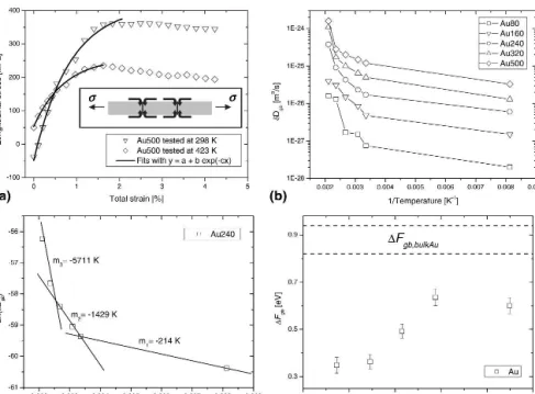
Figure 12(a) shows exemplary fits for two stress– strain curves of Au samples with 500-nm film thickness tested at 298 and 423 K. Obviously, the fit describes the experimental data better for the stress–strain curve meas-ured at higher temperature. Because the model considers only elastic deformation and diffusional creep, the unfa-vorable fit for the room-temperature stress–strain curve indicates that diffusional creep is not active at room tem-perature. This is not unexpected and is also reflected in the values extracted for␦Dgb[Fig. 12(b)]. They increase strongly for temperatures above 373 K and with increas-ing film thickness. In the Arrhenius plot for 240-nm-thick Au samples, three regimes with different slope can be identified [Fig. 12(c)]. The first two regimes reach from 123 to 298 K and from 298 to 373 K. The cor-responding slopes m1 and m2 would give activation en-ergies for grain-boundary diffusion of only 0.02 and 0.12 eV, which again indicates the absence of diffusional creep. The third and steepest regime above 373 K, how-ever, leads to an activation energy of 0.49 eV. The slope of the third regime has been determined for all film thick-nesses and is listed together with the corresponding ac-tivation energies and pre-exponential factors ␦D0,gb in Table II. The activation energy ⌬Fgb is also plotted against the film thickness in Fig. 12(d).
FIG. 12. (a) Stress–strain curves for Au500 samples tested at 298 and 423 K with corresponding fits according to Eq. (6). The inset shows a schematic illustration for grain-boundary diffusional creep in a freestanding foil under tensile stress. (b)␦Dgbversus reciprocal temperature for Au samples with different film thickness. Grain-boundary diffusion is strongly enhanced in thicker films. (c) ln(␦Dgb) versus reciprocal tem-perature for Au240 samples. Three different regimes with different slope can be identified. The activation energy has been only determined for the high temperature regime with the highest slope. (d) Activation energy for grain-boundary diffusion⌬Fgbas function of film thickness. The dashed lines represent the upper and the lower limit of literature values for the activation energy⌬Fgb,bulkfor bulk Au.
Both the activation energy as well as the pre-exponential factor increase with film thickness. The ac-tivation energy increases from 0.35 up to 0.6 eV. This is in any case considerably smaller than reported values for bulk Ag [⌬Fgb,bulkAg≈ 0.88 to 0.93 eV,
33,41
black line in Fig. 12(d)] or Cu (⌬Fgb,bulkCu⳱ 1.06 eV
42
). On the other hand, similar values of about 0.6 eV have been found experimentally for Ag thin films40 and nanocrystalline Cu,43 which have similar melting points as Au. In contrast to⌬Fgb, the pre-exponential factors ␦D0,gb are lower than literature values for bulk materials (Ag: 4.5 × 10⁻¹⁵ m3 /s,33 Cu: 9.7 × 10⁻¹⁵ m3 /s42 ). This is given by the lower temperature dependence due to the lower ac-tivation energy. On the other hand, in the temperature range of our experiments, the determined␦Dgbvalues are considerably higher than those of the bulk materials. In Fig. 13, the␦Dgbvalues for 80-nm-thick Au samples are compared to polycrystalline (pc)42 and nanocrystalline (nc) Cu.43For both, nc Cu and Au films␦Dgbis orders of magnitudes higher than for pc Cu at temperatures below 373 K. The high diffusivities in nanocrystalline materials have often been attributed to the strongly enhanced vol-ume fraction and the non-equilibrum structure of grain boundaries in these materials (for reviews see e.g., Refs.
44 and 45). Similar arguments may possibly hold for the grain boundaries in our films.
Another important diffusion path for diffusional creep in our films is the film–substrate interface. For the ap-plicability of the Gibbs model, diffusion along the Au/ polyimide has to be at least as fast as grain-boundary diffusion. Raj and Ashby46
have studied the correlation of sliding at nonplanar grain boundaries and diffusional creep as well as elastic accommodation. According to their analysis, the sliding rate is higher for a sinusoidal than for a stepped boundary shape and for elastically weak interfaces. In this sense, the interface between an amorphous polymer and a ductile metallic film (like Au on polyimide) is more likely subjected to interfacial slid-ing than an interface between a metal and ceramic layer (like Au and SiNx) or a regular grain boundary within the film.
So far, the origin of the increasing grain boundary diffusivity for increasing thickness of the Au films is not clear [Fig. 12(b)]. Any argument given above would help to explain a decrease in diffusivity. However, according to Eq. (3), the strain rate for diffusional creep strongly depends on the film thickness and grain size of the films. In our experiments the strain rate was constant, and thus for increasing film thickness and grain size, the diffusiv-ity must increase as well. If, for example, the inherent diffusivity of the Au films would be high enough to accommodate the external strain rate by diffusional creep for a 500-nm-thick film, the diffusivity could be lower for a thinner film. This would mean that the stress re-laxation by diffusional creep in the films must be faster than the external strain rate for all film thicknesses and could also explain the phenomenon of the parallel de-crease in diffusivity and activation energy for decreasing film thickness.
In closing, it must be acknowledged that quantitative arguments in support of diffusional creep processes in thin films remain somewhat speculative. Diffusional creep does not leave traces behind and cannot be fol-lowed by microscopic techniques. The numerical consid-erations and experimental findings given here at least support the possibility that it contributes to the strong temperature dependence found in thin films with small grain sizes and weak interfaces.
V. SUMMARY AND CONCLUSION
The temperature and thickness dependence of the me-chanical properties of passivated and unpassivated Au films has been investigated. Tensile tests have been per-formed in the temperature range between 123 and 473 K. The findings can be summarized as follows.
The temperature dependence of the flow stress was considerably stronger for thin films than that previously found in bulk materials.
TABLE II. Arrhenius data for Au samples: The parameter m3 repre-sents the slope of the Arrhenius plot for the temperature regime above 373 K.⌬Fgbis the activation energy for grain-boundary diffusion and ␦D0,gbthe corresponding pre-exponential factor.
Sample m3(K) ⌬Fgb(eV) ␦D0,gb(m3/s) Au80 −4036 0.35 1.1 × 10⁻²² Au160 −4214 0.36 9.1 × 10⁻²² Au240 −5712 0.49 6.7 × 10⁻²⁰ Au320 −7372 0.64 6.2 × 10⁻¹⁸ Au500 −6964 0.60 4.0 × 10⁻¹⁸
FIG. 13. ␦Dgbas function of temperature for Au80 samples as well as poly-43 and nanocrystalline Cu.44 Nanocrystalline Cu shows even higher diffusivities than the Au films.
Film fracture occurred at low and high temperatures. Low-temperature fracture may be due to decreasing duc-tility, whereas high temperature fracture may result from decreasing adhesion.
For passivated Au films and samples with a SiNx in-terlayer, the temperature dependence of the flow stress could be rationalized by thermally activated dislocation glide. However, the activation energy was lower than the bulk value; this was attributed to the different density and arrangement of obstacles in thin films.
For pure Au films on polyimide, the decrease in flow stress is even more pronounced for temperatures above 373 K, and the thickness dependence of the flow stress disappears. An analysis on the basis of a model for grain-boundary diffusional creep of a freestanding foil gives values for the activation energy of about 0.3–0.6 eV, which are again considerably lower than those for the bulk material. The activation energy and diffusivity de-crease with film thickness, which indicates that diffu-sional creep is strongly pronounced in the thinnest films and may accomplish the complete deformation of the film. This is remarkable because the testing temperatures are at most 0.3 of the homologous temperature.
ACKNOWLEDGMENTS
The synchrotron experiments were carried out at the MPI-MF Surface Diffraction beamline at Ang-strömquelle Karlsruhe (ANKA) (Forschungszentrum Karlsruhe, Germany). We thank A. Stierle, R. Weigel, and N. Kasper for their excellent technical support. The sample chamber for the cooling experiments was built during the beamtime at the MPI-MF beamline and could not have been realized without the help from R. Weigel. We like to extend our special thanks to I. Lakemeyer and G. Richter of the MPI Thin Film Laboratory for the preparation of the thin films. We gratefully acknowledge H.D. Carstanjen and his team for giving us the opportu-nity to perform the RBS measurements at the MPI Pel-letron Accelerator as well as B. Heiland, N. Sauer, S. Haag, and C. Solenthaler for their support in FIB and TEM work. We wish to thank J. Kienle and J.G. Schaller of the MPI Low Temperature Services for the advice and construction of parts of the cooling system.
REFERENCES
1. E. Arzt, G. Dehm, P. Gumbsch, O. Kraft, and D. Weiss: Interface controlled plasticity in metals: Dispersion hardening and thin film deformation. Prog. Mater. Sci. 46, 283 (2001).
2. G. Dehm, T.J. Balk, B. von Blanckenhagen, P. Gumbsch, and E. Arzt: Dislocation dynamics in sub-micron confinement: Recent progress in Cu thin film plasticity. Z. Metallkd. 93, 383 (2002). 3. W.D. Nix: Mechanical properties of thin films. Metall. Trans. A
20,2217 (1989).
4. C.V. Thompson: The yield stress of polycrystalline thin films.
J. Mater. Res. 8, 237 (1993).
5. W.D. Nix: Yielding and strain hardening of thin metal films on substrates. Scr. Mater. 39, 545 (1998).
6. B. von Blanckenhagen, P. Gumbsch, and E. Arzt: Dislocation sources in discrete dislocation simulations of thin-film plasticity and the Hall–Petch relation. Modell. Simul. Mater. Sci. Eng. 9, 157 (2001).
7. P. Pant, K.W. Schwarz, and S.P. Baker: Dislocation interactions in thin fcc metal films. Acta Mater. 51, 3243 (2003).
8. A. Needleman, L. Nicola, Y. Xiang, J.J. Vlassak, and E. Van der Giessen: Plastic deformation of freestanding thin films: Experiments and modeling. J. Mech. Phys. Solids 54, 2089 (2006).
9. P.A. Gruber, J. Böhm, F. Onuseit, A. Wanner, R. Spolenak, and E. Arzt: Size effects on yield strength and strain hardening for ultrathin Cu films with and without passivation: A study by syn-chrotron and bulge test techniques. Acta Mater 56, 2318 (2008). 10. G.B. Gibbs: Diffusion creep of a thin foil. Philos. Mag. 13, 589
(1966).
11. H. Gao, L. Zhang, W.D. Nix, C.V. Thompson, and E. Arzt: Crack-like grain-boundary diffusion wedges in thin metal films. Acta
Mater. 47, 2865 (1999).
12. R.P. Vinci, E.M. Zielinski, and J.C. Bravman: Thermal strain and stress in copper thin films. Thin Solid Films 262, 142 (1995). 13. R. Keller, S.P. Baker, and E. Arzt: Quantitative analysis of
strengthening mechanisms in thin Cu films: Effects of film thick-ness, grain size, and passivation. J. Mater. Res. 13, 1307 (1998). 14. D. Weiss, H. Gao, and E. Arzt: Constrained diffusional creep in UHV-produced copper thin films. Acta Mater. 49, 2395 (2001). 15. T.J. Balk, G. Dehm, and E. Arzt: Parallel glide: Unexpected
dis-location motion parallel to the substrate in ultrathin copper films.
Acta Mater. 51, 4471 (2003).
16. L. Sauter: Microstructural and film thickness effects on the ther-momechanical behavior of thin Au films. Ph.D. Thesis, University of Stuttgart, Stuttgart, Germany (2006).
17. M.J. Kobrinsky and C.V. Thompson: Activation volume for in-elastic deformation in polycrystalline Ag thin films. Acta Mater.
48,625 (2000).
18. M.J. Kobrinsky, G. Dehm, C.V. Thompson, and E. Arzt: Effects of thickness on the characteristic length scale of dislocation plas-ticity in Ag thin films. Acta Mater. 49, 3597 (2001).
19. B.N. Lucas and W.C. Oliver: Indentation power-law creep of high-purity indium. Metall. Mater. Trans. A 30, 601 (1999). 20. F.R. Brotzen, C.T. Rosenmayer, C.G. Cofer, and R.J. Gale: Creep
of thin metallic films. Vacuum 41, 1287 (1990).
21. R. Emery, C. Simons, B. Mazin, and G.L. Povirk: High tempera-ture tensile behavior of free-standing gold films, in Thin-Films—
Stresses and Mechanical Properties VII, edited by R.C. Cammarata,
M. Nastasi, E.P. Busso, and W.C. Oliver (Mater. Res. Soc. Symp. Proc. 505, Warrendale, PA, 1998), pp. 57–62.
22. M.A. Haque and M.T.A. Saif: Thermo-mechanical properties of nano-scale freestanding aluminum films. Thin Solid Films 484, 364 (2005).
23. S. Hyun, W.L. Brown, and R.P. Vinci: Thickness and temperature dependence of stress relaxation in nanoscale aluminum films.
Appl. Phys. Lett. 83, 4411 (2003).
24. A.J. Kalkman, A.H. Verbruggen, and G. Janssen: High-temperature bulge-test setup for mechanical testing of free-standing thin films. Rev. Sci. Instrum. 74, 1383 (2003). 25. M. Cieslar, V. Oliva, A. Karimi, and J.L. Martin: Plasticity of thin
Al films as a function of temperature. Mater. Sci. Eng., A 387-389, 734 (2004).
26. J. Böhm, P. Gruber, R. Spolenak, A. Stierle, A. Wanner, and E. Arzt: Tensile testing of ultrathin polycrystalline films: A syn-chrotron-based technique. Rev. Sci. Instrum. 75, 1110 (2004). 27. P. Gruber, J. Böhm, A. Wanner, L. Sauter, R. Spolenak, and
E. Arzt: Size effect on crack formation in Cu/Ta and Ta/Cu/Ta thin film systems, in Nanoscale Materials and Modeling–
Relations Among Processing, Microstructure and Mechanical Properties, edited by P.M. Anderson, T. Foecke, A. Misra, and
R.E. Rudd (Mater. Res. Soc. Symp. Proc. 821, Warrendale, PA, 2004), P2.7.
28. P.A. Gruber, E. Arzt and R. Spolenak: Brittle-to-ductile transition in ultrathin Ta/Cu film systems. J. Mater. Res. (submitted). 29. J.L. Beuth, Jr.: Cracking of thin bonded films in residual tension.
Int. J. Solids Struct. 29, 1657 (1992).
30. Z.C. Xia and J.W. Hutchinson: Crack patterns in thin films.
J. Mech. Phys. Solids 48, 1107 (2000).
31. T. Li, Z.Y. Huang, Z.C. Xi, S.P. Lacour, S. Wagner, and Z. Suo: Delocalizing strain in a thin metal film on a polymer substrate.
Mech. Mater. 37, 261 (2005).
32. Y. Xiang, T. Li, Z.G. Suo, and J.J. Vlassak: High ductility of a metal film adherent on a polymer substrate. Appl. Phys. Lett. 87, 61910 (2005).
33. H.J. Frost and M.F. Ashby, Deormation-Mechanism Maps: The
Plasticity and Creep of Metals and Ceramics (Pergamon Press,
Oxford, UK, 1982).
34. P.A. Gruber, C. Solenthaler, E. Arzt, and R. Spolenak: Strong single-crystalline Au films tested by a new synchrotron technique.
Acta Mater. 56, 1876 (2008).
35. S.H. Oh, M. Legros, D. Kiener, P. Gruber, and G. Dehm: In situ TEM straining of single crystal Au films on polyimide: Change of deformation mechanisms at the nanoscale. Acta Mater. 55, 5558 (2007).
36. G. Dehm, D. Weiss, and E. Arzt: In situ transmission-electron-microscopy study of thermal-stress-induced dislocations in a thin Cu film constrained by a Si substrate. Mater. Sci. Eng., A 309-310, 468 (2001).
37. B. von Blanckenhagen, P. Gumbsch, and E. Arzt: Dislocation sources and the flow stress of polycrystalline thin metal films.
Philos. Mag. Lett. 83, 1 (2003).
38. D.S. Gianola, S. Van Petegem, M. Legros, S. Brandstetter, H. Van Swygenhoven, and K.J. Hemker: Stress-assisted discon-tinuous grain growth and its effect on the deformation behavior of nanocrystalline aluminum thin films. Acta Mater. 54, 2253 (2006).
39. M.D. Thouless: Effect of surface diffusion on the creep of thin films and sintered arrays of particles. Acta Metall. Mater. 41, 1057 (1993).
40. M.J. Kobrinsky and C.V. Thompson: The thickness dependence of the flow stress of capped and uncapped polycrystalline Ag thin films. Appl. Phys. Lett. 73, 2429 (1998).
41. A. Gangulee and F.M. Dheurle: Activation-energy for electromi-gration and grain-boundary self-diffusion in gold. Scr. Metall. 7, 1027 (1973).
42. W. Gust, S. Mayer, A. Bogel, and B. Predel: Generalized repre-sentation of grain-boundary self-diffusion data. J. Phys. E 46, 537 (1985).
43. J. Horvath, R. Birringer, and H. Gleiter: Diffusion in nanocrys-talline material. Solid State Commun. 62, 319 (1987).
44. R. Birringer, H. Hahn, H. Hofler, J. Karch, and H. Gleiter: Diffusion and low temperature deformation by diffusional creep of nanocrystalline materials. Diffusion and defect data—Solid state data. Part A. Defect and Diffusion Forum 59, 17 (1988). 45. R. Wurschum, S. Herth, and U. Brossmann: Diffusion in
nanocrystalline metals and alloys—A status report. Adv. Eng.
Mater. 5, 365 (2003).
46. R. Raj and M.F. Ashby: On grain boundary sliding and diffusional creep. Metall. Trans. 2, 1113 (1971).