HAL Id: hal-00806026
https://hal.archives-ouvertes.fr/hal-00806026
Submitted on 29 Mar 2013
HAL is a multi-disciplinary open access
archive for the deposit and dissemination of
sci-entific research documents, whether they are
pub-lished or not. The documents may come from
teaching and research institutions in France or
abroad, or from public or private research centers.
L’archive ouverte pluridisciplinaire HAL, est
destinée au dépôt et à la diffusion de documents
scientifiques de niveau recherche, publiés ou non,
émanant des établissements d’enseignement et de
recherche français ou étrangers, des laboratoires
publics ou privés.
The Apparent Constant-Phase-Element Behavior of an
Ideally Polarized Blocking Electrode
Vicky Mei-Wen Huang, Vincent Vivier, Mark E. Orazem, Nadine Pébère,
Bernard Tribollet
To cite this version:
Vicky Mei-Wen Huang, Vincent Vivier, Mark E. Orazem, Nadine Pébère, Bernard Tribollet. The
Ap-parent Constant-Phase-Element Behavior of an Ideally Polarized Blocking Electrode. Journal of The
Electrochemical Society, Electrochemical Society, 2007, vol. 154, pp.C81-C88. �10.1149/1.2398882�.
�hal-00806026�
O
pen
A
rchive
T
oulouse
A
rchive
O
uverte (
OATAO
)
OATAO is an open access repository that collects the work of Toulouse researchers and
makes it freely available over the web where possible.
This is an author-deposited version published in:
http://oatao.univ-toulouse.fr/
Eprints ID : 2417
To link to this article :
URL :
http://dx.doi.org/10.1149/1.2398882
To cite this version :
Huang , Vicky Mei-Wen and Vivier , Vincent and Orazem,
Mark E. and Pébère, Nadine and Tribollet, Bernard ( 2007)
The Apparent
Constant-Phase-Element Behavior of an Ideally Polarized Blocking Electrode.
Journal of The Electrochemical Society (JES), vol. 154 (n° 2). C81-C88. ISSN
0013-4651
Any correspondence concerning this service should be sent to the repository
administrator: [email protected]
The Apparent Constant-Phase-Element Behavior of an Ideally
Polarized Blocking Electrode
A Global and Local Impedance Analysis
Vicky Mei-Wen Huang,a,
*
Vincent Vivier,b,**
Mark E. Orazem,a,***
,zNadine Pébère,c,
**
and Bernard Tribolletb,**
a
Department of Chemical Engineering, University of Florida, Gainesville, Florida 32611, USA b
UPR15 du CNRS, Laboratoire Interfaces et Systèmes Electrochimiques, Université Pierre et Marie Curie, 75252 Paris, France
c
CIRIMAT, UMR CNRS 5085, ENSIACET, 31077 Toulouse Cedex 04, France
Two numerical methods were used to calculate the influence of geometry-induced current and potential distributions on the impedance response of an ideally polarized disk electrode. A coherent notation is proposed for local and global impedance which accounts for global, local, local interfacial, and both global and local ohmic impedances. The local and ohmic impedances are shown to provide insight into the frequency dispersion associated with the geometry of disk electrodes. The high-frequency global impedance response has the appearance of a constant-phase element共CPE兲 but can be considered to be only an apparent CPE because the CPE exponent␣ is a function of frequency.
关DOI: 10.1149/1.2398882兴
Both primary and secondary current and potential distributions associated with the disk geometry have been developed by Newman.1,2The primary distribution applies when the current and potential are governed by the ohmic resistance to current flow in the electrolyte. The secondary distribution applies when both ohmic and kinetic resistances are controlling. In the absence of faradaic reac-tions and for very short time scales, the primary current distribution associated with the charging of an electrode surface can be expected to follow i 具i典= 1 2
冑
1 −冉
r r0冊
2 关1兴where r0 is the radius of the disk and 具i典 is the average current
density on the electrode. In the absence of mass-transfer limitations, the transient response of a disk electrode requires the solution of Laplace’s equation with flux conditions at the electrode surface.
Nisancioglu and Newman3,4 have developed a solution for the transient response of a faradaic reaction on a nonpolarizable disk electrode to step changes in current. The solution to Laplace’s equa-tion was performed using a transformaequa-tion to rotaequa-tional elliptic co-ordinates and a series expansion in terms of Legendre polynomials. Antohi and Scherson have recently expanded the solution to the transient problem by expanding the number of terms used in the series expansion.5
The solutions described above account for the relaxation of the potential at the electrode surface.3-5Conversely, the solution pre-sented by Oldham6is incorrect because it assumes that the fixed-potential condition at the electrode surface applies for all time scales and that the local ohmic impedance is therefore a real number ob-tained from the primary current distribution共Eq. 1兲.
The impedance response of electrodes rarely show the ideal re-sponse expected for single electrochemical reactions. The imped-ance response typically reflects a distribution of reactivity that is commonly represented in equivalent electrical circuits as a constant phase element共CPE兲.7-9For a blocking electrode, the CPE can be represented as
Z共f兲 = Re+
1
共j2f兲␣Q 关2兴
where the parameters ␣ and Q are constants. When ␣ = 1, Q has units of a capacitance, i.e.,F/cm2, and represents the capacity of
the interface. When␣ ⫽ 1, the system shows behavior that has been attributed to surface heterogeneity10,11or to continuously distributed time constants for charge-transfer reactions.12-16 The phase angle associated with a CPE is independent of frequency.
Using both global and local impedance measurements on a mag-nesium alloy, Jorcin et al.17have shown that the geometry of a disk in an insulating plane can induce CPE behavior and that this CPE behavior can be associated with a radial distribution of local resis-tance. The authors suggested that these results could be explained in terms of the numerical and analytic treatment for the impedance response of a disk electrode presented in 1970 by Newman.18
The objective of this work was to explore the role of current and potential distributions on the global impedance response of an ide-ally polarized electrode and to relate this response to the local im-pedance. Subsequent papers will address the influence of current and potential distributions on the impedance response of systems exhib-iting local CPE behavior19共i.e., coupled 2D and 3D distributions兲 and faradaic reactions.20
2D and 3D Distributions
Frequency dispersion leading to CPE behavior can be attributed to distributions of time constants along either the area of the elec-trode共involving only a two-dimensional surface兲 or along the axis normal to the electrode surface共involving a three-dimensional as-pect of the electrode兲. A 2D distribution could arise from surface heterogeneities such as grain boundaries, crystal faces on a poly-crystalline electrode, or other variations in surface properties. The frequency dispersion associated with geometry-induced nonuniform current and potential distributions results from a 2D distribution.
CPE behavior may also arise from a variation of properties in the direction that is normal to the electrode surface. Such variability may be attributed, for example, to changes in the conductivity of oxide layers21-23 or from porosity or surface roughness.24,25 This CPE behavior is said to arise from a 3D distribution, with the third direction being the direction normal to the plane of the electrode.17 A schematic representation of a 2D distribution for an ideally polarized disk electrode is presented in Fig. 1a. For a 2D distribu-tion, the circuit parameters, e.g., capacitance and ohmic resistance, could be a function of radial position along the electrode. Integration
*Electrochemical Society Student Member.
**Electrochemical Society Active Member.
***Electrochemical Society Fellow.
z
of the admittance associated with these circuit elements would yield a global impedance with a CPE behavior. The local impedance, in the case of a 2D distribution, would, however, show ideal behavior. A 3D distribution of blocking components in terms of resistors and constant-phase elements is presented in Fig. 1b. Such a system yields a local impedance with a CPE behavior, even in the absence of a 2D distribution of surface properties. If the 3D system shown schematically in Fig. 1b is influenced by a 2D distribution, the local impedance should reveal a variation of CPE coefficients along the surface of the electrode. Thus, local impedance measurements can be used to distinguish whether the CPE behavior arises from a 2D distribution, from a 3D distribution, or from a combined 2D and 3D distribution.
Using both global and local impedance measurements on a disk made of AZ91 magnesium alloy, Jorcin et al.17found CPE behavior that was attributed to a 2D distribution, which yielded locally a pure capacitive response coupled with a radial distribution of local resis-tance. Jorcin et al.17have also found CPE behavior on a pure alu-minum disk in which the local impedance response showed a CPE which was modified only slightly by an apparent 2D distribution.
Mathematical Development
The steady-state solution for the current distribution at a block-ing electrode is that the current is equal to zero. The primary current distribution given as Eq. 1 therefore applies, not at the steady state, but at infinite frequency. This situation differs from the special case of a faradaic system with an ohmic resistance that is much larger than the kinetic resistance and for which Eq. 1 provides the steady-state current distribution.
The object of this work was to calculate, from first principles, the influence of geometry-induced current and potential distributions on the impedance response of a disk electrode. The mathematical de-velopment follows that presented by Newman.18Laplace’s equation in cylindrical coordinates was expressed in rotational elliptic coor-dinates, i.e.
y = r0 关3兴
and
r = r0
冑
共1 + 2兲共1 − 2兲 关4兴where 0ⱕ ⱕ ⬁ and 0 ⱕ ⱕ 1. Within the revised coordinate system, the electrode surface at y = 0 and rⱕ r0can be found at = 0 and 0 ⱕ ⱕ 1. The reference electrode and counter electrode located at r→ ⬁ can be found at → ⬁. The insulating surface of the disk at y = 0 and r⬎ r0is located at = 1 and 0 ⬍ ⱕ ⬁, and
the center line at y⬎ 0 and r = 0 is located at = 0 and 0 ⬍ ⱕ ⬁.
Laplace’s equation can be expressed in rotational elliptic coordi-nates as
冋
共1 + 2兲 ⌽ 册
+ 冋
共1 − 2兲 ⌽ 册
= 0 关5兴 The potential was separated into steady and time-varying parts as⌽ = ⌽¯ + Re关⌽˜ exp共jt兲兴 关6兴 where⌽¯ is the steady-state solution for potential and ⌽˜ is the com-plex oscillating potential. Thus, Eq. 5 could be written as
2 ⌽ ˜ r +共1 + 2兲 2⌽˜ r 2 − 2 ⌽˜ r +共1 − 2兲 2⌽˜ r 2 = 0 关7兴 and 2 ⌽ ˜ j +共1 + 2兲 2⌽˜ j 2 − 2 ⌽˜ j +共1 − 2兲 2⌽˜ j 2 = 0 关8兴
where⌽˜rand⌽˜jrefer to the real and imaginary parts of the com-plex oscillating potential, respectively.
The flux boundary condition at the electrode surface共 = 0 and 0ⱕ ⱕ 1兲 is i = C0 共V − ⌽0兲 t = −
冏
⌽ y冏
y=0 = − r0冏
⌽ 冏
=0 关9兴where C0is the interfacial capacitance and is the electrolyte
con-ductivity. Equation 9 was written in frequency domain as K⌽˜j= − 1
冏
⌽˜ r 冏
=0 关10兴 and KV˜r− K⌽˜r= − 1 冏
⌽˜ j 冏
=0 关11兴where V˜rrepresents the imposed perturbation in the electrode poten-tial referenced to an electrode at infinity and K is the dimensionless frequency
K = C0r0
关12兴
At = 0 and = 1, for all ⬎ 0, zero-flux conditions impose that ⌽˜ r = 0 关13兴 and ⌽˜ j = 0 关14兴
At the far boundary condition共 → ⬁ and 0 ⱕ ⱕ 1兲 ⌽˜
r= 0 关15兴
and
Figure 1. Schematic representation of an impedance distribution for a
block-ing disk electrode where Rerepresents the ohmic resistance, C0represents
the interfacial capacitance, and z0represents an interfacial impedance corre-sponding to Eq. 2:共a兲 2D distribution of blocking components in terms of resistors and capacitors and共b兲 3D distribution of blocking components in terms of resistors and CPEs.
⌽˜
j= 0 关16兴
The equations were solved under the assumption of a uniform ca-pacitance C0 using the collocation package PDE2D developed by Sewell.26Calculations were performed for differing domain sizes, and the results reported here were obtained by extrapolation to an infinite domain size.
The equations were also solved in the cylindrical coordinates using a finite-elements package FEMLAB. The results obtained by the two packages were in excellent agreement for dimensionless frequencies K⬍ 100.
Definition of Terms
The global impedance results presented in the following section can be understood through examination of the local impedance dis-tribution. As there are several types of local impedance at play, discussion of local impedance requires clear notation and defini-tions.
A schematic representation of the electrode–electrolyte interface is given as Fig. 2, where the block used to represent the local ohmic impedance reflects the complex character of the ohmic contribution to the local impedance response. The impedance definitions pre-sented in Table I differ in the potential and current used to calculate the impedance. To avoid confusion with local impedance values, the symbol y is used to designate the axial position in cylindrical coor-dinates.
Global impedance.— The global impedance is defined to be
Z =V ˜ I
˜ 关17兴
where the complex current contribution is given by I
˜ =
冕
0
r0
i˜共r兲2rdr 关18兴 The use of an upper-case letter signifies that Z is a global value. The global impedance may have real and imaginary values designated as Zrand Zj, respectively. The total current could also be represented
by I˜ = r02具i˜共r兲典, where the brackets signify the area-average of the current density.
Local impedance.— The term local impedance traditionally in-volves the potential of the electrode measured relative to a reference electrode far from the electrode surface.27,28Thus, the local imped-ance is given by
z = V ˜
i˜共r兲 关19兴
The use of a lower-case letter signifies that z is a local value. The local impedance may have real and imaginary values designated as zrand zj, respectively.
The global impedance can be expressed in terms of the local impedance as
Z =
冓
1 z冔
−1
关20兴 Equation 20 is consistent with the treatment of Brug et al.7in which the admittance of the disk electrode was obtained by integration of a local admittance over the area of the disk.
Local interfacial impedance.— The local interfacial impedance involves the potential of the electrode measured relative to a refer-ence electrode⌽0共r兲 located at the outer limit of the diffuse double
layer. Thus, the local interfacial impedance is given by z0=V˜ − ⌽
˜
0共r兲
i˜共r兲 关21兴
The use of a lower-case letter again signifies that z0is a local value, and the subscript 0 signifies that z0 represents a value associated
only with the surface. The local interfacial impedance may have real and imaginary values designated as z0,rand z0,j, respectively.
Local ohmic impedance.— The local ohmic impedance involves the potential of a reference electrode⌽˜0共r兲 located at the outer limit
of the diffuse double layer and the potential of a reference electrode located far from the electrode⌽˜ 共⬁兲 = 0 共see Fig. 2兲. Thus, the local ohmic impedance is given by
ze=
⌽˜
0共r兲
i˜共r兲 关22兴
The use of a lower-case letter again signifies that zeis a local value,
and the subscript e signifies that ze represents a value associated only with the ohmic character of the electrolyte. The local ohmic
Table I. Notation proposed for local impedance variables.
Symbol Meaning Units
Z global impedance共Eq. 17兲 ⍀ or ⍀ cm2
Zr real part of global impedance ⍀ or ⍀ cm2
Zj imaginary part of global impedance ⍀ or ⍀ cm2
Z0 global interfacial impedance共Eq. 24兲 ⍀ or ⍀ cm2
Z0,r real part of global interfacial impedance ⍀ or ⍀ cm2
Z0,j imaginary part of global interfacial impedance ⍀ or ⍀ cm2
Ze global ohmic impedance共Eq. 26兲 ⍀ or ⍀ cm2
Ze,r real part of global ohmic impedance ⍀ or ⍀ cm2
Ze,j imaginary part of global ohmic impedance ⍀ or ⍀ cm2
z local impedance共Eq. 19兲 ⍀ cm2
zr real part of local impedance ⍀ cm2
zj imaginary part of local impedance ⍀ cm2
z0 local interfacial impedance共Eq. 21兲 ⍀ cm2
z0,r real part of local interfacial impedance ⍀ cm2
z0,j imaginary part of local interfacial impedance ⍀ cm2
ze local ohmic impedance共Eq. 22兲 ⍀ cm2
ze,r real part of local ohmic impedance ⍀ cm2
ze,j imaginary part of local ohmic impedance ⍀ cm2
具⌽典 spatial average of potential V
⌽¯ time average or steady-state value of potential V
具i典 spatial average of current density A/cm2
i¯ time average or steady-state value of current density A/cm2
y axial position variable cm
Figure 2. The location of current and potential terms that make up
impedance may have real and imaginary values designated as ze,r
and ze,j, respectively. The local impedance
z = z0+ ze 关23兴
can be represented by the sum of local interfacial and local ohmic impedances.
The representation of an ohmic impedance as a complex number represents a departure from standard practice, and the related in-sights constitute a major contribution of the present work. As is shown in subsequent sections, the local impedance has inductive features that are not seen in the local interfacial impedance. As the calculations assumed an ideally polarized blocking electrode, the result is not influenced by faradaic reactions and can be attributed only to the ohmic contribution of the electrolyte.
Global interfacial impedance.— The global interfacial imped-ance is defined to be Z0= 2
冉
冕
0 r0 1 z0共r兲rdr冊
−1 关24兴 or Z0=冓
1 z0共r兲冔
−1 关25兴 The use of an upper-case letter signifies that Z0 is a global value. The global interfacial impedance may have real and imaginary val-ues designated as Z0,rand Z0,j, respectively.Global ohmic impedance.— The global ohmic impedance is de-fined to be
Ze= Z − Z0 关26兴
The use of an upper-case letter signifies that Z is a global value. As is shown in subsequent sections, the global ohmic impedance has a complex behavior in a mid-frequency range共near K = 1兲. The glo-bal ohmic impedance may have real and imaginary values desig-nated as Ze,rand Ze,j, respectively.
Results and Discussion
The calculated results for global, local, local interfacial, and both local and global ohmic impedances are presented in this section. The results of both the collocation and finite element method 共FEM兲 methods were in perfect agreement for frequencies K⬍ 100.
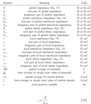
Global impedance.— The global impedance response presented in Fig. 3a shows the influence of frequency dispersion at frequencies K⬎ 1. This dispersion is seen as a deviation from the vertical line obtained for low frequencies共K ⬍ 1兲. The expanded logarithmic representation presented in Fig. 3b shows the agreement with the numerical solutions presented by Newman.18 The impedance is made dimensionless according to Z/r0, in which the units of im-pedance Z are scaled by unit area, for example,⍀ cm2.
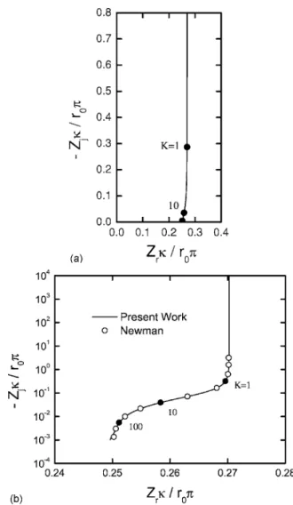
The comparison with Newman’s calculations is seen more clearly in the representation of the real and imaginary parts of the impedance response shown in Fig. 4a and b, respectively. As dis-cussed by Orazem et al.,29 the change in the slope of the lines presented in Fig. 4b shows that the impedance response transitions from ideal RC behavior at low frequencies to a CPE-like behavior at frequencies K⬎ 1. The slope is equal to −␣, the exponent of the CPE presented in Eq. 2. A deviation from Newman’s results is seen for both the collocation and FEM calculations for frequencies K ⬎ 100. This error is attributed to a singular perturbation problem that arises at the periphery of the electrode at high frequencies.18
The value of −␣, which is equal to the slope of the log共Zj/r0兲 with respect to log共K兲, is presented in Fig. 5 as a function of dimen-sionless frequency K. The numerical results obtained by collocation and FEM methods is compared to the asymptotic limit developed by Newman using a singular perturbation approach. The system be-haves as an ideal capacitor at low frequencies K⬍ 1 with ␣ = 1. At
frequencies K⬎ 1, the value of alpha changes to roughly ␣ = 0.85 before beginning a gradual return towards unity. As the slope is not independent of frequency, the frequency dispersion seen at K⬎ 1 does not represent true CPE behavior.
The frequency K = 1 at which the current and potential distribu-tions begin to influence the impedance response can be expressed as
f = 2C0r0
关27兴 or, in terms of electrolyte resistance, as
f = 1 8C0Re
关28兴 As shown in Fig. 6, this characteristic frequency can be well within the range of experimental measurements. The value /C0 = 104cm/s can be obtained for a capacitance C0= 1F/cm2
共cor-responding to an oxide layer兲 and conductivity = 0.01 S/cm 共cor-responding to a 0.1 M NaCl solution兲. The value /C = 103cm/s
can be obtained for a capacitance C0= 10F/cm2共corresponding
to the double layer on an inert metal electrode兲 and conductivity = 0.01 S/cm 共corresponding to a 0.1 M NaCl solution兲. Figure 6 can be used to show that, by using an electrode that is sufficiently small, the experimentalist may be able to avoid the frequency range that is influenced by current and potential distributions.
Figure 3. Calculated Nyquist representation of the impedance response for
an ideally polarized disk electrode:共a兲 linear plot showing effect of disper-sion at frequencies K⬎ 1 as a deviation from a vertical line and 共b兲 loga-rithmic scale showing agreement with the calculations of Newman.
Local interfacial impedance.— The calculated local interfacial impedance is presented in Fig. 7a as a function of frequency with position as a parameter and in Fig. 7b as a function of position with
frequency as a parameter. All four curves indicated in Fig. 7a and b, respectively, are superposed. The results presented in Fig. 7 show that the local interfacial impedance is that associated with a pure capacitive behavior. At all frequencies, z0,jK/r0 = 1/ as is ex-pected for an ideal capacitance. The real part of the local interfacial impedance, not shown here, was equal to zero within computational accuracy.
Figure 4. Calculated representation of the impedance response for an ideally
polarized disk electrode:共a兲 real part and 共b兲 imaginary part showing agree-ment with the calculations and asymptotic formula of Newman.
Figure 5. The slope of log共Zj/r0兲 with respect to log共K兲 共Fig. 4b兲 as a
function of log共K兲. The results were calculated by the collocation method, by FEM methods, and by using the asymptotic formula of Newman. The value of this slope is equal to −␣.
Figure 6. The frequency K =1 at which the current distribution influences
the impedance response with/C0as a parameter.
Figure 7. Calculated imaginary part of the local interfacial impedance:共a兲 as
a function of frequency with position as a parameter and共b兲 as a function of position with frequency as a parameter. All four curves indicated in Fig. 7a and b, respectively, are superposed.
Local impedance.— The calculated local impedance response is presented in Fig. 8 in Nyquist format with radial position as a pa-rameter. The dimensionless impedance is scaled to the disk arear02 in order to show the comparison with the asymptotic value of 0.25 for the real part of the dimensionless impedance. The impedance is largest at the center of the disk and smallest at the periphery, reflect-ing the greater accessibility of the periphery of the disk electrode. Inductive loops are seen at high frequencies, and these were ob-tained by both methods of calculation.
The real and imaginary parts of the local impedance are pre-sented in Fig. 9a and b, respectively, with radial position as a pa-rameter. The real part of the local impedance presented in Fig. 9a reaches asymptotic values at K→ 0 and K → ⬁. The imaginary part presented in Fig. 9b shows the change of sign associated with the inductive features seen in Fig. 8. The changes in sign occur at frequencies well below K = 100, showing that the inductive loop cannot be ascribed to a calculation artifact. The deviation from ideal capacitive behavior for frequencies K⬎ 1 is similar to that seen in Fig. 4b for the imaginary part of the global impedance.
The radial distribution of the real and imaginary impedance is presented in Fig. 10a and b, respectively, with dimensionless fre-quency K as a parameter. At high frequencies, e.g., K = 100, the calculated radial distribution of the real part of the local impedance follows the expression
zr r0
冉
r r0冊
= 0.5冑
1 −冉
r r0冊
2 关29兴 derived from Eq. 1 using the expression for the primary resistance1 in the formRe=
1 4r0r0
2 关30兴
The radial distribution for the imaginary part of the impedance de-viates from ideal capacitive behavior for frequencies K⬎ 1.
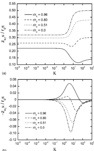
Local ohmic impedance.— Following Eq. 23, the local ohmic impedance zeaccounts for the difference between the local interfa-cial and local impedances. As the local interfainterfa-cial impedance
corre-sponds to a pure capacitor, the term zecannot be a pure electrolyte resistance Re. The calculated local ohmic impedance is presented in
Fig. 11 in Nyquist format with radial position as a parameter. The shape of the diagrams are strongly dependent on the position on the electrode. At the periphery of the electrode, two time constants 共in-ductive and capacitive loops兲 are seen, whereas at the electrode center only an inductive loop is evident. These loops are distributed around the asymptotic value of 1/4. The calculated values for real and imaginary parts of the local ohmic impedance are presented in Fig. 12a and b, respectively, as a function of frequency, with radial position as a parameter. The local ohmic impedance has only real values at K→ 0 and K → ⬁, but in the frequency range 10−2
⬍ K ⬍ 100, zehas both real and imaginary components. Figure 12a
clearly shows the asymptotic behavior in the low frequency range with values distributed around 1/4.
Global interfacial and global ohmic impedance.— The local in-terfacial impedance is associated with a pure capacitance that is independent of radial position. Thus, the global interfacial imped-ance arises from a pure capacitimped-ance C0 in units of F/cm2. The
global ohmic impedance Zeis obtained from the global impedance Z by the expression
Ze= Z −
1
jC0 关31兴
or, in the dimensionless terms used in the present work
Figure 8. The local impedance in Nyquist format with radial position as a
parameter.
Figure 9. Calculated local impedance with radial position as a parameter:共a兲
Ze r0= Z r0 − 1 jK 关32兴
The real part of Zeis equal to the real part of Z as given in Fig. 4a. The imaginary part of Zeis given in Fig. 13 as a function of
dimen-sionless frequency K. In the low frequency range Zeis a pure resis-tance equal to 1.08Re, and in the high frequency range Ze tends
towards Re.
The imaginary part of the global ohmic impedance shows a non-zero value in the frequency range that is influenced by the current and potential distributions. Figures 4a and 13 show that all the ef-fects of the current and potential distribution appears in the global ohmic impedance.
At high and low frequency limits, the global ohmic impedance defined in the present work is consistent with the accepted under-standing of the ohmic resistance to current flow to a disk electrode. The global ohmic impedance approaches, at high frequencies, the primary resistance for a disk electrode 共Eq. 30兲 described by
Figure 10. Calculated local impedance as a function of radial position:共a兲
real part and共b兲 imaginary part multiplied by dimensionless frequency K. The solid line is given in Fig. 10b to indicate the axis at zj= 0.
Figure 11. The local ohmic impedance in Nyquist format with radial
posi-tion as a parameter.
Figure 12. Calculated values for local ohmic impedance as a function of
frequency with radial position as a parameter:共a兲 real part and 共b兲 imaginary part. The solid line is given in Fig. 12b to indicate the axis at ze,j= 0.
Figure 13. The imaginary part of the global ohmic impedance, calculated
Newman.1The global ohmic impedance approaches, at low frequen-cies, the value for the ohmic resistance calculated by Newman18for a disk electrode.
The complex nature of both the global and local ohmic imped-ances is seen at intermediate frequencies. This complex value is the origin of the inductive features calculated for the local impedance and the quasi-CPE behavior found at high frequency for the global impedance.
Conclusions
The global impedance for an ideally polarized disk electrode is influenced by current and potential distributions at high frequencies. While the local interfacial impedance shows the expected ideally polarized behavior, the local impedance shows inductive behavior at high frequency and ideal behavior at low frequency. The local im-pedance is influenced by the local ohmic imim-pedance, which has complex behavior near dimensionless frequency K = 1. The imagi-nary part of both the local and global ohmic impedance is equal to zero at both high and low frequencies where the ohmic impedance has purely resistive character.
The explanation of the frequency dispersion requires a coherent notation for local and global impedance which accounts for global, local, local interfacial, and both the local and global ohmic imped-ances. A notation is proposed in Table I that extends terms found in the local impedance literature to account for both local ohmic and local interfacial impedances.
The local and global ohmic impedance is shown to provide in-sight into the frequency dispersion associated with the geometry of disk electrodes. The high-frequency impedance response has the ap-pearance of a CPE but can be considered to be only an apparent CPE because the CPE exponent␣ is not independent of frequency.
Acknowledgment
The authors gratefully acknowledge the financial support of their home institutions, which facilitated this collaboration.
Centre National de la Recherche Scientifique assisted in meeting the publication costs of this article.
References
1. J. S. Newman, J. Electrochem. Soc., 113, 501共1966兲. 2. J. S. Newman, J. Electrochem. Soc., 113, 1235共1966兲.
3. K. Nisancioglu and J. Newman, J. Electrochem. Soc., 120, 1339共1973兲. 4. K. Nisancioglu and J. Newman, J. Electrochem. Soc., 121, 523共1974兲. 5. P. Antohi and D. A. Scherson, J. Electrochem. Soc., 153, E17共2006兲. 6. K. B. Oldham, Electrochem. Commun., 6, 210共2004兲.
7. G. J. Brug, A. L. G. van den Eeden, M. Sluyters-Rehbach, and J. H. Sluyters, J. Electroanal. Chem. Interfacial Electrochem., 176, 275共1984兲.
8. J. R. Macdonald, Impedance Spectroscopy: Emphasizing Solid Materials and Sys-tems, John Wiley & Sons, New York共1987兲.
9. A. Lasia, in Modern Aspects of Electrochemistry, Vol. 32 R. E. White, B. E. Con-way, and J. O. Bockris, Editors, p. 143, Plenum Press, New York共1999兲. 10. Z. Lukacs, J. Electroanal. Chem., 432, 79共1997兲.
11. Z. Lukacs, J. Electroanal. Chem., 464, 68共1999兲. 12. J. R. Macdonald, J. Appl. Phys., 58, 1971共1985兲. 13. J. R. Macdonald, J. Appl. Phys., 58, 1955共1985兲.
14. R. L. Hurt and J. R. Macdonald, Solid State Ionics, 20, 111共1986兲. 15. J. R. Macdonald, J. Appl. Phys., 62, R51共1987兲.
16. J. R. Macdonald, J. Electroanal. Chem., 378, 17共1994兲.
17. J.-B. Jorcin, M. E. Orazem, N. Pébère, and B. Tribollet, Electrochim. Acta, 51, 1473共2006兲.
18. J. S. Newman, J. Electrochem. Soc., 117, 198共1970兲.
19. V. M.-W. Huang, V. Vivier, I. Frateur, M. E. Orazem, and B. Tribollet, J. Electro-chem. Soc., 154, C89共2006兲.
20. V. M.-W. Huang, V. Vivier, M. E. Orazem, N. Pébère, and B. Tribollet, J. Electro-chem. Soc., 154, C99共2006兲.
21. L. Young, Trans. Faraday Soc., 51, 1250共1955兲.
22. L. Young, Anodic Oxide Films, Academic Press, New York共1961兲. 23. C. A. Schiller and W. Strunz, Electrochim. Acta, 46, 3619共2001兲.
24. R. Jurczakowski, C. Hitz, and A. Lasia, J. Electroanal. Chem., 572, 355共2004兲. 25. T. Pajkossy, Solid State Ionics, 176, 1997共2005兲.
26. G. Sewell, The Numerical Solution of Ordinary and Partial Differential Equations, John Wiley & Sons, New York共2005兲.
27. R. S. Lillard, P. J. Moran, and H. S. Isaacs, J. Electrochem. Soc., 139, 1007共1992兲. 28. F. Zou, D. Thierry, and H. S. Isaacs, J. Electrochem. Soc., 144, 1957共1997兲. 29. M. E. Orazem, N. Pébère, and B. Tribollet, J. Electrochem. Soc., 153, B129