HAL Id: hal-00591004
https://hal.archives-ouvertes.fr/hal-00591004
Submitted on 6 May 2011HAL is a multi-disciplinary open access
archive for the deposit and dissemination of sci-entific research documents, whether they are pub-lished or not. The documents may come from teaching and research institutions in France or abroad, or from public or private research centers.
L’archive ouverte pluridisciplinaire HAL, est destinée au dépôt et à la diffusion de documents scientifiques de niveau recherche, publiés ou non, émanant des établissements d’enseignement et de recherche français ou étrangers, des laboratoires publics ou privés.
A Largely Reconfigurable Impulse Radio UWB
Transceiver
Aubin Lecointre, Daniela Dragomirescu, Robert Plana
To cite this version:
Aubin Lecointre, Daniela Dragomirescu, Robert Plana. A Largely Reconfigurable Impulse Radio UWB Transceiver. Electronics Letters, IET, 2010, 46 (6), p.453-455. �hal-00591004�
A Largely Reconfigurable Impulse Radio UWB
Transceiver
A. Lecointre, D. Dragomirescu and R. Plana
This letter presents a new and efficient digital baseband architecture for impulse radio ultra wideband (IR-UWB) transceivers with reconfigurable capacities for wireless sensor network (WSN) applications. An implementation is done on FPGA for validation by measurements. It achieves the highest data rate and the largest number of operating modes for an IR-UWB reconfigurable transceiver, to the best of the author’s knowledge. Measurements demonstrate reconfigurability in data rate (from 4 to 125 MBits/s), chip duration (from 8 to 32 ns), pulse duration (from 1 to 4 ns), bit duration (from 8 to 256 ns), processing gain (from 1 to 8 pulses/bit), occupied bandwidth, radio range, BER performance, synchronization accuracy (from 0.5 to 4 ns), pulse amplitude, transmitted power density, duty cycle (from 3 to 50 %), power consumption, spectrum occupation, and maximum supported UWB channel delay spread (from 4 to 31 ns).
Introduction:
IR-UWB is well known to be a radio technology which answers WSN requirements thanks to the use of low duty cycle transmissions [1]. IR-UWB advantages’ are low size, low complexity and low cost, as well as the possibility of low power implementation [1]. This letter presents a dynamically reconfigurable IR-UWB digital baseband transceiver, for fulfilling efficiently the
large needs of WSN applications, at the best cost at any time even with some changes in the operating conditions, the local regulation, or the radio channel behavior.
Implemented IR-UWB transceivers reconfigurable in multiple properties are rare in literature. Reference [2] demonstrates a pulse modulation and data rate reconfigurable FPGA based IR-UWB transceiver. Reference [3] presents an IR-UWB transceiver reconfigurable in data rate (up to 30 Mbits/s), pulse duration, occupied bandwidth and modulation. The most complete IR-UWB reconfigurable transceiver is introduced in [4]. Its reconfigurability is in data rate (up to 50 Mbits/s), processing gain, and synchronization algorithm. Thus it has the ability to adjust its radio range, bit error rate (BER) performance, power consumption and spectrum occupation.
The proposed IR-UWB transceiver:
The proposed IR-UWB reconfigurable digital baseband is implemented on FPGA using VHDL. Analog-to-digital and digital-to-analog converters (ADC/DAC) are used for interfacing the digital baseband and the radio frequency (RF) front-end. The proposed transceiver uses BPSK modulation and a direct spread spectrum technique. Thanks to its time domain signal processing, IR-UWB is well suited for a digital implementation, and thus lends itself to the implementation of reconfigurability. Each property (the bit duration
Tb, the chip duration Tc, the pulse duration Tp, the synchronization accuracy
Sa) of the transceiver can be defined by reconfigurable input parameters M*x
time resolution is defined by the ADC/DAC performance. For example, the reconfigurability in chip duration Tc is expressed as
Tc = M*Tc x r. (1)
By adjusting the reconfigurable input parameter values M*x, the transceiver
can dynamically change its properties. This scheme is applied for the pulse duration, the chip duration, the bit duration and the synchronization accuracy. These four basic reconfigurability parameters imply also reconfigurability in data rate, processing gain, BER performance, synchronization performance, duty cycle, power consumption, spectrum shape, supported channel delay spread, and radio range. In addition, by being able to change the output pulse amplitude, reconfigurability in emitted power and in compliance with local regulations is added to the IR-UWB transceiver.
The digital baseband transmitter is designed for driving a high speed time interleaved DAC. The transmitter comprises a data generator block which generates a frame with a start frame delimiter (SFD) and a payload data field. A BPSK pulse generator and a spreading block are also implemented. The spreading block is dedicated to map the data with the spread spectrum sequence. The BPSK pulse generator drives the DAC with a signal of length
Tp (pulse duration) at either the positive full scale range or the negative full
scale range.
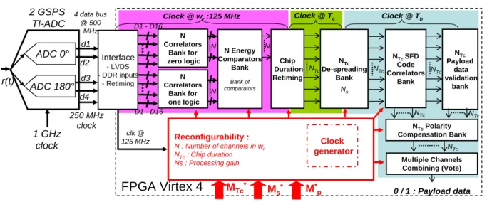
The digital baseband receiver implementation is presented in the fig. 1. The proposed reconfigurable BPSK IR-UWB receiver is a coherent Rake-like receiver with parallel search frame level synchronization on N bins. These N bins are used for covering the synchronization search space. The length of a bin is equal to the synchronization accuracy Sa. For each bin, the receiver
dedicates two cross correlators, an energy comparator, a de-spreading block and a SFD code correlator to carry out a first bit demodulation and the frame level synchronization. In function of the N SFD code correlators outputs, Nsync outputs are considered as frame level synchronized outputs and can be seen as fingers of the Rake. From the N bins, the receiver selects Nsync fingers on a frame level synchronization criteria. A vote procedure combines the Nsync correlators outputs for improving the signal to noise ratio and the BER performance. The output bit value is equal to the value of the majority of the
Nsync correlators outputs. It’s a high level (bit level after frame synchronization)
combining technique.
To allow reconfigurability based on a time domain signal processing, a chip duration retiming block, a clock generator block are necessary as well as a
block for dealing with the reconfigurability parameters M*x, at both the
transmitter and the receiver side.
Reconfigurability measurements results:
Due to the higher complexity of the receiver with respect to the transmitter, the overall performance is limited by the receiver implementation. The synchronization accuracy, the chip duration and the pulse duration of the transceiver directly impact the size of the circuit. The number and the range of features are limited by the hardware, i.e. the size of the FPGA, and the sampling frequency of the DAC and ADC.
Two Xilinx Virtex4lx15 FPGAs are used for baseband implementation, one for the transmitter and one for the receiver. A 1 GSPS DAC, a 2 GSPS ADC and RF blocks are commercial off-the-shelf (COTS) components. The RF
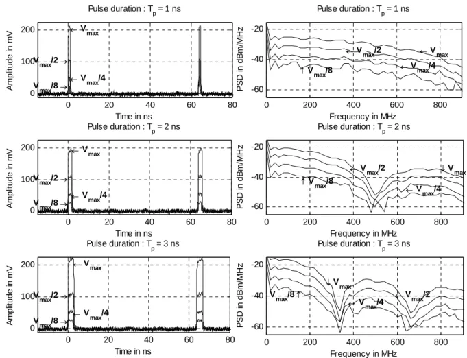
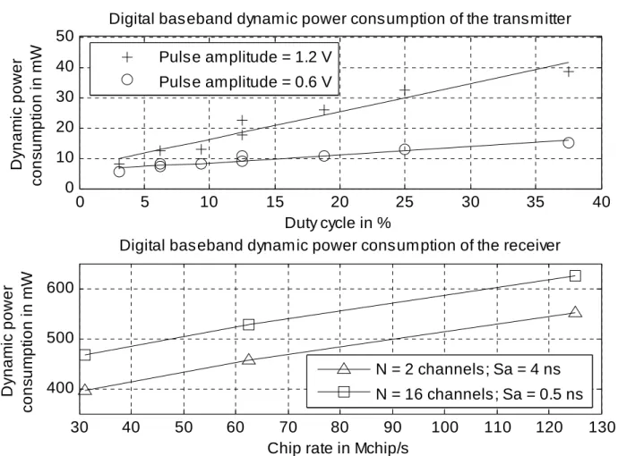
front-end contains LNA, PA, filters, antennas and up- and down-conversion stages centred at 3.9 GHz. Measurements are made in an industrial environment. The transmitter-receiver distance is 4 meters. The SNR is changed thanks to digital step attenuator in the receiver RF front-end. The measurements in fig. 2 to 4 show the vast reconfigurability (48 distinct operating modes) of the implemented IR-UWB transceiver. The implemented transceiver achieves reconfigurability in chip duration (8 to 32 ns), bit duration (8 to 256 ns), data rate (4 to 125 Mbits/s), processing gain (1 to 8 pulses/bit), pulse duration (1 to 4 ns) (fig. 2), pulse amplitude (25 to 200 mV) (fig. 2), occupied bandwidth (250 MHz to 1 GHz) (fig. 2), transmitted power density (fig. 2), radio range (fig. 2), BER performances (fig. 3), synchronization accuracy (0.5 to 4 ns) (fig. 3), synchronization performances (fig. 3), duty cycle (3 to 50 %), power consumption (fig. 4), and maximum supported UWB channel delay spread (4 to 31 ns). Fig. 3 presents the reconfigurability in synchronization accuracy, demodulation performance (BER) and synchronization performance, versus
the Eb/N0 measured at the FPGA receiver input. By reconfiguring its
synchronization accuracy itself from 4 to 0.5 ns, the proposed transceiver
achieves a gain of 6 dB in Eb/N0 for the synchronization, and a gain of 5 dB in
Eb/N0 for a 6.10-5 BER level. The radio range is thus also reconfigurable. Link
budget calculations show distinct ways for using the available dB obtained thanks to reconfigurability. For example, as illustrated by the fig. 4, the 4 ns synchronization accuracy allows a 72 mW decrease of the FPGA receiver dynamic power consumption in comparison with the 0.5 ns synchronization accuracy. These measurements demonstrate the validity of the proposed reconfigurable IR-UWB digital baseband transceiver architecture. The
transceiver offers a larger range of reconfigurable properties and a higher data rate than the transceivers presented in [2]-[3]-[4].
Conclusion: A new and efficient IR-UWB reconfigurable transceiver
architecture for digital baseband is proposed. Validation implementation is done on FPGA. Measurements show that the implemented reconfigurable IR-UWB transceiver achieves the largest number of reconfigurable properties and the highest data rate, i.e. 125 Mbits/s, for a reconfigurable UWB transceiver to the best author’s knowledge. It allows to the radio to use its best operating parameters for answering any kind of change in the environment (channel response, communication range, energy available, local regulation, and applications needs). The proposed transceiver architecture and implementation are well suited for wireless sensor networks applications with time-variant operating performance requirements.
References
1 L. Yang and G. B. Giannakis: ‘Ultra-wideband communications, an idea whose time has come’, IEEE Signal Processing Magazine, pp. 26-54, November 2004.
2 C. Anderson and J. Reed: ‘A software defined ultra wideband communication system testbed’, Virginia Space Grant Consortium Student Research Conference, 2006.
3 I. D. O’Donnel and R. Brodersen: ’A flexible, low power, DC-1GHz impulse-UWB transceiver front-end’, IEEE International Conference on Ultra-Wideband, ICUWB 2006, pp. 275-279.
4 M. Verhelst, J. Ryckaert, Y. Vanderperren, and W. Dehaene: ‘A low power, reconfigurable IR-UWB system’, IEEE International Conference on Communications, ICC 2008, pp. 3770-3774.
A. Lecointre, D. Dragomirescu, and R. Plana. (CNRS ; LAAS ; 7 avenue du colonel Roche, F-31077 Toulouse, France ; Université de Toulouse ; UPS, INSA, INP, ISAE ; LAAS ; F-31077 Toulouse, France) [email protected], [email protected], [email protected].
Figure captions:
Fig. 1 The proposed reconfigurable BPSK IR-UWB receiver digital baseband implementation.
Fig. 2 Pulse duration, pulse amplitude, occupied bandwidth and power spectral density reconfigurability measurements.
Fig. 3 Synchronization and BER performances reconfigurability measurements in function of the synchronization accuracy and the number of channels N over a multipath indoor channel.
Fig. 4 Dynamic power consumption reconfigurability measurements of the digital baseband for both the transmitter and the receiver side.
Figure 1 2 GSPS TI-ADC r(t) ADC 180° ADC 0° 1 GHz clock FPGA Virtex 4 Interface - LVDS - DDR inputs - Retiming 250 MHz clock Reconfigurability : N : Number of channels in wr NTc: Chip duration Ns : Processing gain 4 data bus @ 500 MHz d1 d2 d3 d4 Clock @ wr:125 MHz D1 - D16 0 / 1 : Payload data clk @ 125 MHz N Correlators Bank for
zero logic Chip
Duration Retiming NTc De-spreading Bank NTcSFD Code Correlators Bank NTc Payload data validation bank NTcPolarity Compensation Bank Multiple Channels Combining (Vote) N Energy Comparators Bank Bank of comparators Clock generator Clock @ Tc Clock @ Tb N NTc Ns N N NTc NTc NTc NTc NTc Ms* M * p MTc* N Correlators Bank for one logic D1 - D16
Figure 2 0 20 40 60 80 0 100 200 V max Vmax/2 Vmax/4 Vmax/8 Time in ns A m p lit u d e in m V Pulse duration : Tp = 1 ns 0 200 400 600 800 -60 -40 -20 Vmax Vmax/2 V max/4 V max/8 Frequency in MHz P S D in dB m/ MH z Pulse duration : Tp = 1 ns 0 20 40 60 80 0 100 200 Vmax Vmax/2 Vmax/4 Vmax/8 Time in ns A m p lit u d e in m V Pulse duration : Tp = 2 ns 0 200 400 600 800 -60 -40 -20 Vmax Vmax/2 V max/4 V max/8 Frequency in MHz P S D in dB m/ MH z Pulse duration : Tp = 2 ns 0 20 40 60 80 0 100 200 V max Vmax/2 Vmax/4 Vmax/8 Time in ns A m p lit u d e in m V Pulse duration : Tp = 3 ns 0 200 400 600 800 -60 -40 -20 V max Vmax/4 Vmax/2 V max/8 Frequency in MHz P S D in dB m/MH z Pulse duration : Tp = 3 ns
Figure 3 -6 -4 -2 0 2 4 0 50 100 E b/N0 in dB P a c k et det ec ti on r a te in %
Synchronization performance evolution with reconfigurability
-6 -4 -2 0 2 4 10-4 10-2 E b/N0 in dB BE R
Demodulation performance evolution with reconfigurability
N=16; Sa=0.5ns. N=8; Sa=1ns. N=4; Sa=2ns. N=2; Sa=4ns.
Figure 4 0 5 10 15 20 25 30 35 40 0 10 20 30 40 50 Duty cycle in % Dy nam ic power c o ns um pt ion in m W
Digital baseband dynamic power consumption of the transmitter Pulse amplitude = 1.2 V Pulse amplitude = 0.6 V 30 40 50 60 70 80 90 100 110 120 130 400 500 600
Chip rate in Mchip/s
Dy nam ic power c o ns um pt ion in m W
Digital baseband dynamic power consumption of the receiver
N = 2 channels; Sa = 4 ns N = 16 channels; Sa = 0.5 ns