A Ballistic Transport Model for HEMTs and
III-V
MOSFETs
by
Shireen M. Warnock
B.S. Electrical Engineering
Massachusetts Institute of Technology, 2011
SUBMITTED TO THE DEPARTMENT OF ELECTRICAL ENGINEERING AND COMPUTER SCIENCE IN PARTIAL FULFILLMENT OF THE REQUIREMENTS FOR THE
DEGREE OF
MASTER OF ENGINEERING IN ELECTRICAL ENGINEERING AT THE
MASSACHUSETTS INSTITUTE OF TECHNOLOGY
FEBRUARY 2013
0 2013 Shireen M. Warnock. All rights reserved.
The author hereby grants to MIT permission to reproduce and to distribute publicly paper and electronic copies of this thesis document in whole or in part in any medium now known or
hereafter created.
Signature of author:
Department of Electrical Engineering and Computer Science February 1, 2013 Certified by:
Accepted by:
Jesis A. del Alamo Professor of Electrical Engineering Thesis Supervisor
Dennis M. Freeman Professor of Electrical Engineering Chairman, Masters of Engineering Thesis Committee
A Ballistic Transport Model for HEMTs and
I1-V
MOSFETs
by
Shireen M. Warnock
Submitted to the Department of Electrical Engineering and Computer Science February 1, 2013
in Partial Fulfillment of the Requirements for the Degree of Master of Engineering in Electrical Engineering
ABSTRACT
As silicon MOSFETs keep scaling down in size, the continued improvement on their logic performance is threated by their fundamental physical limits. With silicon approaching these limits, MOSFETs designed with III-V semiconductors have emerged as promising candidates to replace them. The low-effective mass of various III-V materials such as InGaAs and InAs allow both faster and more power efficient performance.
One of the key challenges, particularly as devices continue to shrink, is to understand the
important of non-idealities in FET structures. High-electron mobility transistors, or HEMTs, are III-V Quantum-Well FETs that we can use to explore many issues of relevance to future III-V MOSFETs. HEMTs are worthwhile transistors in their own right, but are also simpler than III-V MOSFETs and therefore allow a more thorough exploration into the basic transport physics of a quantum-well III-V device.
We know from HEMT experimental data that electrons travel ballistically at gate lengths of 30-40 nm, suggesting that a ballistic transport model will only become more accurate as channel lengths are scaled down to 10 nm. We would like to investigate to what extent this is true in III-V MOSFETs, and also to study the impact of short channel effects and other parasitics inherent to a III-V design.
To accomplish these goals, we have developed a flexible transistor model in MATLAB based on a ballistic theory of transport. We will first verify the model with HEMT experimental data coming from devices fabricated at MIT, and then focus our attention on peculiarities specific to III-V MOSFETs, namely a buried-channel design and the presence of traps at the
oxide-semiconductor interface. We will use the model to extract the trap density as a function of
energy, and then make measurements independent of interface trap effects to extract the 2D sheet carrier concentration and mobility, two figures of merit important in characterizing FET devices. The ability to correctly model and predict device behavior will help identify the problems ahead that need improvement in the iterations of future device fabrication.
Thesis supervisor: Jesu's A. del Alamo Title: Professor of Electrical Engineering
Acknowledgements
I would first of all like to thank my research supervisor Jesu's A. del Alamo for giving me the opportunity to work on such an exciting research topic and to be involved in such an interesting field of study. His guidance and depth of knowledge have really allowed me to grow as a researcher, and I could not have asked for a better advisor.
Many thanks also go to Jianqing Lin, Dr. Tae-Woo Kim, and Ling Xia for the devices they were so kind to share with me for my experimental work and for their helpful discussions in getting me started and making sure I was always on the right track. I would similarly like to express thanks to Winston Chern for his many helpful conversations and the valuable samples he gave me as well.
I would also like to extend thanks to members of the Francis Bitter Magnet Laboratory, particularly Jagadeesh Moodera, Peng Wei, and Marius Eich. They always took time to teach and help in any way they could, making themselves available and making me feel like I was a part of the Magnet Lab family.
I am very appreciative of the other members of the del Alamo research group-Donghyun Jin, Luke Guo, and Xin Zhao, who have provided me with valuable insight not only into research but have given me advice on gradual school and life in general. I look forward to continuing my work with them and all the new members of the group.
I would like to thank my closest friends for their never-ending support: Naomi Jiang, Clark Davenport, Clara Bennett, Alex Guo, and Chase Anderson.
Lastly, I would like to thank my family, without whose love and help none of this would have been possible.
Contents
LIST OF FIGURES ... 9
CHAPTER 1. INTRODUCTION... 11
1.1 Introduction to HEM Ts and III-V CM OS ... 11
1.2 M otivation- A Compact M odel For Device Studies ... 14
1.3 Thesis Outline ... 15
CHAPTER 2. CURRENT-VOLTAGE THEORETICAL MODEL... 17
2.1 Introduction ... 17
2.2 Previous Work... ... ... 17
2.2.1 Current in a Ballistic Quantum -W ell FET... 17
2.2.2 Gate Capacitance ... 21
2.3 I-V M odel for HEM T ... 22
2.3.1 Sim ulation Process Flow ... 23
2.3.2 Impact of the Drain on n, and vj ... 24
2.3.3 Parasitic Resistances: Source, Drain, and Access ... 25
2.3.4 Non-parabolic Band Structure... 27
2.3.5 Drain-Induced Barrier Lowering ... 28
2.3.6 Self-heating ... 29
2.3.7 Ballisticity Factor ... 30
2.4 III-V M OSFE T: Additions to the HEM T M odel ... 32
2.4.1 Interface State Traps... 33
2.4.2 Surface-Channel M OSFET ... 34
2.4.3 Buried-Channel M OSFET... 35
2.5 Sum m ary ... 36
CHAPTER 3. SIMULATION RESULTS & EXPERIMENTAL WORK ... 39
3.1 Introduction ... 39
3.2 Device Under Study ... 39
3.3 Sim ulation Study of Parameters ... 40
3.3.1 Significance of m * ... 40
3.3.2 Impact of Nonparabolicity... 43
3.3.3 Effect of Rcs, RCD, and Raccess ... ... ... 44
3.4 Comparison with Experimental Data ... 45
3.4.1 Transfer Characteristics... 45
3.4.2 Output Characteristics ... 50
3.5 Sum mary ... 51
CHAPTER 4. C-V CHARACTERISTICS & Dit: Ill-V MOSFET ... 53
4.1 4.2 4.3 4.4 4.5 Introduction ... 53
Quantum Capacitance M odel ... 53
D evice Under Study ... 55
Effect of D i on Subthreshold Swing ... 56
Comparison with Experim ental D ata ... 58
4.6 H all Effect M easurem ents... 67
4.6.1 Theory for the Hall Effect ... 67
4.6.2 p and n, for the III-V Quantum -W ell M OSFET... 69
4.7 Sum m ary ... 72
CHAPTER 5. CONCLUSIONS AND SUGGESTIONS... 75
5.1 Conclusions ... 75
List of Figures
Figure 1-1. Schematic of a HEMT structure, reproduced from D. Jin et al. [5]. The red dotted line in the schematic indicates the location of the 6 doping layer, and the channel consists
of either InG aA s or InA s... 12
Figure 1-2. Schematic of a MOSFET structure, reproduced from J. Lin et al. [6]. The black layer represents a thin high-K dielectric, and the 6 doping layer is located underneath the ch an n el. ... 13
Figure 2-1 Energy band diagram for a QW-FET. The first sub-band is depicted as EI, and the Fermi level in the material as EF. The surface potential is shown as s. ... 18
Figure 2-2 Conduction band along the length of the channel, for high drain bias, reproduced from [10]. Electrons injected from source and drain are labeled by arrows...19
Figure 2-3 Model of the different factors that contribute to gate capacitance...21
Figure 2-4 I-V characteristics of a 30 nm InAs HEMT compared with the HEMT theoretical m odel, reproduced from [11] ... 22
Figure 2-5 Conduction band simulation of a HEMT in nextnano under flatband conditions, with VGS=O. The conduction band (black) as well as the quantum sub-bands El and E2 (blue and green) is plotted with respect to the Fermi level (red). ... 23
Figure 2-6 Cross-section of a simplified HEMT device. Rs and RD are defined between the source and drain, and Raccess is symmetric on both sides of the intrinsic region...26
Figure 2-7 Variation of peak temperature as a function of VDS and VGs, reproduced from [17]..29
Figure 2-8 Potential profile from source to drain for large VDS. The potential drop of (kT/q) is labeled in red with the corresponding kT-layer f in orange... 31
Figure 2-9 Dit across the energy gap, shown in blue. The filled states are those below the Fermi lev e l...3 3 Figure 2-10 Gate capacitance model for surface-channel MOSFET. Cs, CD, and Cit are as previously defined, and Cis is the oxide capacitance...34
Figure 2-11 Gate capacitance model for buried-channel MOSFET. Capacitances are as previously defined, and Cbarrier is due to the barrier layer between the channel and oxide.35 Figure 3-1 Schematic of a HEMT structure, reproduced from D. Jin et al. [5]...39
Figure 3-2 Effect of m* on ns (left) and vinj (right). Arrows indicate direction of increasing m*. 41 Figure 3-3 Effect of m* on ID (top left), gm (top right), and gate capacitance CG (bottom). Arrows indicate direction of increasing m *. ... 42
Figure 3-4 Effect of a on ns, vinj, and ID- Arrows indicate the direction of increasing a...43
Figure 3-5 ID and gm vs. VGS for Rcs # 0 (top), RCD # 0 (middle), and Raccess # 0 (bottom). ... 46
Figure 3-6 gm for several values of m*, plotted against experimental gm. ... 47
Figure 3-7 Subthreshold simulated vs. experimental data...48
Figure 3-8 Transfer characteristics of simulation vs. experiment: I-V characteristics (left), and transconductance (right)... 49
Figure 3-9 Output characteristics of simulation vs. experiment, for extrinsic device parameters
extracted from transfer characteristics ... ...50
Figure 3-10 Output characteristics of simulation vs. experiment, for extrinsic parameters to match output conductance...51
Figure 4-1 Equivalent circuit diagram for quantum capacitance modeled, from D. Jin et al. [5].54 Figure 4-2. Schematic of a MOSFET structure, reproduced from J. Lin et al. [6]...55
Figure 4-3 Qualitative graph of the different Dit distributions explored in this study...56
Figure 4-4 ID vS. VGS in the subthreshold regime (logarithmic scale). Ideal case of perfect subthreshold swing is shown in blue. ... 57
Figure 4-5 ID vS. VGS in the saturation regime. Ideal case of perfect subthreshold swing is shown in b lu e...--- ---... 5 8 Figure 4-6 C-V characteristics of simulation (smooth lines) plotted against experiment (marked lines) for A1203 oxide, -65'C. The simulated CG is in blue, the quantum capacitance CQI of the first sub-band in green, the inversion capacitance of the first sub-band in aqua, and the second inversion capacitance in purple. The value of the A1203 capacitance Ci1 is plotted as the black dashed line for reference... 59
Figure 4-7 C-V characteristics of simulation plotted against experiment for HfD2 oxide, -65 C..61
Figure 4-8 C-V characteristics of simulation with Dit = 0 against experiment for A1203 oxide, room tem perature...- -- -- --- ---... 62
Figure 4-9 C-V characteristics of simulation & experiment for A1203 with Di, fit. ... 63
Figure 4-10 Dit distribution for A1203 in the InP band gap, extracted from C-V. ... 64
Figure 4-11 Dit distribution in the InP band gap, reproduced from [23]. ... 65
Figure 4-12 Room temperature C-V for simulation vs. experiment for Hft 2 (top left), C-V for simulation fitted with Di, (top right), Dit distribution in InP bandgap (bottom). ... 66
Figure 4-13 Schem atic of a simple Hall bar. ... 67
Figure 4-14 Sheet resistance (top right), sheet carrier concentration (middle right), and mobility (bottom right) for A1203 device. ... 70
Figure 4-15 Sheet resistance (top right), sheet carrier concentration (middle right), and mobility (bottom right) for HfO2 device. ... ... 71
CHAPTER 1. INTRODUCTION
Moore's law demands that logic devices must continue to shrink, but silicon-based MOSFETs are fast approaching their fundamental limits and may not be a viable option for gate lengths below 10 nm [1]. MOSFETs designed with III-V semiconductors, however, have become promising candidates to replace them. Their improved transport properties and efficiency stem from the low-effective mass of typical Ill-V materials such as InAs or InGaAs. In this study, we will explore not only the Ill-V MOSFET but also the III-V high electron mobility transistor, or HEMT. The HEMT will give us insight into the fundamental transport properties common to all quantum-well FETs, and from there we can address the unique characteristics that arise from the presence of an oxide layer in the III-V MOSFET.
1.1 Introduction to III-V HEMTs and MOSFE Ts
Whereas many traditional semiconductor devices use p-n homojunctions, high electron mobility transistors exploit the characteristics of a heterojunction. The use of a large-bandgap, highly doped material next to an undoped, narrow-bandgap material creates sheet of electrons within which the electrons can move with far less scattering and a higher velocity. This concept of modulation doping, where there is a spatial separation between the dopants and the electrons, results in the formation of a two-dimensional electron gas (2DEG) at the interface between the different bandgap materials [2]. The electrons in the quantum well have a high mobility and can move quickly without colliding with any impurities, due to the fact that the channel is made out of an undoped material.
Commonly used material combinations for HEMTs include AlGaAs/GaAs, AlGaN/GaN, and InAlAs/InGaAs. These pairs are chosen by the need to have a close lattice match but also large conduction band discontinuity between the two materials, and the specific pair is determined by the desired device application be it high power or high frequency performance. In this work, we
will study InAlAs/InGaAs HEMTs. Figure 1-1 shows the schematic for a typical HEMT structure. An InAlAs buffer layer is grown on top of an InP substrate, and the channel is either InAs or InGaAs with a high-indium content, surrounded by InGaAs cladding layers. The choice of an InAs or InO.7Gao.3As channel is because both materials have been shown to exhibit high injection velocities and relatively low effective mass [3]. Above the channel is an InAlAs barrier layer with a 6 doping layer of Si that provides carriers to the channel. The highly doped InGaAs
capping layer improves the contact resistance of the HEMT.
There are various aspects of the HEMT to consider when characterizing its operation. A few key parameters of the device include Lg, the gate length, Lside, the distance between the edge of the gate and the edge of the cap as depicted in Figure 1-1, and both the channel and barrier thicknesses. These parameters greatly impact many figures of merit important to HEMTs, including the transconductance gm that is a measure of how steeply the current rises above threshold, and the subthreshold swing, which is the rate of the current drop-off below the threshold voltage VT. The drain-induced barrier lowering (DIBL) which is the dependence of the threshold voltage on the drain-to-source voltage VDs is another parameter of interest. Parasitic resistances and capacitances inherent to the structure of the material also play a role in determining the operational behavior of the HEMTs [3],[4].
S
D
ChWnnl InO.5GaOVAr (2 nm)
Chnnel= InolGao3As (8 nm)
... or InAs (5 nm )
tb ChWMnn.ln3GSOaAS (3 rn
Figure 1-1. Schematic of a HEMT structure, reproduced from D. Jin et al. [5]. The red dotted line in the schematic indicates the location of the 6 doping layer, and the channel consists of either
Until now, HEMTs have been used in high speed and high frequency applications, but not for logic applications. They cannot present a viable alternative to silicon-based logic devices because of their high gate leakage current. III-V quantum-well MOSFETs address this problem by inserting an oxide layer between the gate and the barrier layer, as shown in Figure 1-2. In fact, III-V MOSFETs employing high-K dielectrics are already in development and have been demonstrated with excellent performance [5, p. 2], making them promising candidates for future generations of CMOS technology. However, the presence of the oxide layer introduces a density of interface state traps, Dit, that can degrade the subthreshold swing and yield a poorer ION/LOFF ratio [7].
It is important, then, to consider not only the device characterization of HEMTs, but also the unique issues that arise in the transition from III-V HEMTs to MOSFETs. These two objectives will be the focus of this study.
Figure 1-2. Schematic of a MOSFET structure, reproduced from J. Lin et al. [6]. The black layer
1.2 Motivation - A Compact Model for Device Studies
As discussed above, there are many characteristics of a transistor, both intrinsic and extrinsic, that will have an effect on device performance. This leads to the desire for a flexible, compact model based on the ballistic transport of electrons as a 2DEG, which at 30 nm gate lengths, should be an accurate representation of the current in a FET and which will only become more accurate as channel lengths are scaled down to 10 nm. Experimental verification of this assumption comes from devices fabricated at MIT, where the source injection velocity of electrons at gate lengths of 30-40 nm is seen to approach saturation [3]. The saturation of the injection velocity suggests that the HEMT devices are close to operating in a purely ballistic regime.
One goal of this project is to develop a hybrid approach where the quantum-mechanical portion of the simulation, through means of Poisson-Schr6dinger simulations, is accurate but the device transport is simplified and short-channel effects are neglected so as to focus on the role of various parasitics, such as DIBL, subthreshold swing, etc., in limiting device performance.
A need also exists to explore the non-idealities of III-V quantum-well MOSFET structures; in particular, the presence of charge interface states and their impact on the I-V characteristics is a phenomenon that has not been fully studied. We can use C-V measurements to characterize the device and extract the sheet carrier concentration and mobility, n, and t respectively. However, because Dit has an impact on the C-V characteristics as well, it is important to be able to obtain n, and pt over a range of gate voltages through techniques independent of Dit, and to juxtapose them with the measured C-V characteristics. In this way, a Dit profile could be extracted and compared with other methodologies of finding interface trap densities [8].
A common way to extract the concentration of mobile charge in a 2D structure is to perform Hall measurements. Using a Hall bar, we can measure the differential voltage, or Hall voltage, in the presence of a magnetic field when current is injected down the length of the bar. This voltage, VHall, as well a determination of the sheet resistance, will yield the values of mobile charge and mobility independently. With a gated Hall bar, n, and p can be found across all regimes of
operation and compared with experimental C-V to yield a complete picture of Dit. The second goal of this study, therefore, will be to construct a complete capacitance-voltage model that accurately incorporates the role of Dit and to compare this against measurements on actual structures.
1.3 Thesis Outline
In this project, we develop a compact transistor model in MATLAB. This HEMT current-voltage model is based on ballistic transport and incorporates many parasitic elements such as DIBL and source and drain resistances with the intent of exploring the impact of these parasitics on device behavior.
We also build upon an existing quantum capacitance model for HEMTs [5] to incorporate Dit effects, and compare experimental C-V characteristics with simulated ones. As an integral piece of the C-V work, gated Hall measurements were carried out that resulted in extracted mobilities significantly higher than those measured by split C-V techniques [6].
This thesis is organized in the following way. Chapter 2 is a detailed theoretical discussion of both the ballistic current model and the gate capacitance model. The central physics of ballistic transport are outlined and a simulation process flow is introduced that allows the incorporation of non-idealities, each of which are also discussed in detail. The gate capacitance model is also described for both HEMTs and III-V MOSFETs. This theory results in a comprehensive framework against which experimental data can be compared.
In Chapter 3 we present the results of the theoretical model as they relate to the HEMT. We first discuss several important non-idealities, such as the effect of non-parabolic bands on the output and transfer characteristics. Then, we compare the simulated data against experimental data for HEMT devices.
Chapter 4 investigates the characteristics of the MOSFET, focusing first briefly on the effect of Dit on the I-V characteristics and in particular, the subthreshold swing. The primary focus of
Chapter 4, however, is to compare the C-V data for III-V MOSFETs against the quantum capacitance model, and to use this to extract Dit. To complement these results and demonstrate how large of an effect Dit can have on device figures of merit, conventional gated Hall measurements were performed and values of 2DEG sheet carrier concentration and channel mobility were obtained.
To conclude in Chapter 5, we summarize the results of this work on a ballistic compact model, and provide suggestions for future work in the field of III-V FET characterization.
CHAPTER 2. I-V THEORETICAL MODEL
2.1 Introduction
In this chapter, we use Poisson-Schrbdinger simulations to construct the current-voltage characteristics of both HEMTs and III-V MOSFETs. For this, we have developed a ballistic transport model. The peculiarities associated with MOSFETs are discussed separately as additions to the model for the HEMT.
2.2 Previous Work
2.2.1 Current in a Ballistic Quantum-Well FET
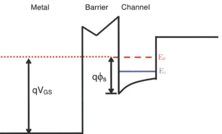
In a HEMT, electrons move in the undoped, narrow-bandgap channel material with minimal scattering. This is due to their spatial separation with the 6 doping layer in the barrier that provides the free carriers (see Figure 1-1: the 6 doping layer is located in the barrier, and carrier transport occurs inside the channel). For short enough gate lengths, the electrons actually travel at a ballistic velocity, where they do not scatter at all as they move through the channel. A detailed calculation of the current in a QW-FET is covered by [9], and summarized below.
For a QW-FET, the electrons are confined in one direction (normal to the wafer surface) and therefore create a two-dimensional electron gas. To simplify the analysis, we assume that only a single sub-band in the channel is occupied, as shown in Figure 2-1. This is actually the case in deeply scaled HEMTs and MOSFETs operating close to the peak transconductance point. The level labeled E1 is the bottom of the first 2D energy band that arises as a result of the quantum
well structure of the channel. EF is the location of the Fermi level in the material, whose level is extended beyond the channel for reference. The discontinuity in the barrier arises from the 6 doping layer, and we define the surface potential
4s
as the distance between the Fermi level andMetal Barrier Channel
9 s El
qVGS s
-Figure 2-1 Energy band diagram for a QW-FET. The first sub-band is depicted as E1, and the
Fermi level in the material as EF. The surface potential is shown as <s.
The 2D density of states in the sub-band is known to be:
92D(E) = (1)
m* is the effective mass of the electrons in the channel material, and h is the reduced Planck's constant. The sheet carrier concentration, n,, which is needed in order to find the current in the FET, can be found by integrating the product of g2D and the Fermi function f(E):
Jm*
7'
dEni=r2hE (~d 2 _..__ (2)
El ir 2E 1 1 +e kT
k is Boltzmann's constant, and T is the temperature of the material. Solving this integral yields the following simple expression:
ns = N2030 (3)
where N2D is the 2D effective density of states, m*kT
N2D = 2
Z30(x) = In (1 + ex) (5)
Figure 2-2 illustrates the concept of the virtual source model, where the current is limited by the injection of electrons over the barrier at the source [10]. For a high enough drain voltage, we assume there will be no back flow of electrons from the channel or the drain past the injection point.
Gate
Source
Drain
Figure 2-2 Conduction band along the length of the channel, for high drain bias, reproduced from [10]. Electrons injected from source and drain are labeled by arrows.
For such high drain biases, all the electrons at the virtual source contribute to the current, making the expression for current in the FET simply:
ID = qnsvinj (6)
where viaj, the injection velocity, is the average velocity of the electrons as they move towards
the drain. vinj can be found by computing v(E) for electrons in the channel, integrating over E, and then dividing by the number of electrons. If we consider the channel to be oriented in the x-direction, then the velocity of electrons at a given energy E is given by [9]:
2 2(E -E 1)
vx(E) = - , (7)
To find the injection velocity, we must consider both the occupation and the density of states at every energy E, and properly normalize:
SfjE 92D(E)vx(E)f(E)dE (8) fE1 92D(E)f(E)dE This yields: 1 EF - E1 Vin; =- VT EF - E (9) 30 kTE
where we have simplified the expression using the following definitions:
2kT
S= , (10)
2 fc
31/2(X = o1+e -XdE 1
where VT is the thermal velocity, F'1/ is the Fermi-Dirac integral of order one-half, and:
E -E 1
E = (12)
kT
Combining Eqs. 3, 6 and 9 yields the final expression for the drain current:
ID= qN2DVT3 1/2 (EFEkT) (13)
The Fermi-Dirac integrals for both n, and vij can be simplified in the non-degenerate limit where
EF-El «< 1 to give a much simpler expression for the drain current. However, the HEMT operates
kT
in degenerate conditions where the Fermi level is close to or above the first sub-band E, and therefore we cannot take the non-degenerate limit of these expressions.
Measurements or predictions of the drain current, ID, are important when studying both the output and transfer characteristics of a HEMT for logic purposes. Therefore, it is vital to have a
working model of ID to provide a basis for understanding experimental data and for verifying that the theory adequately describes the observed behavior.
2.2.2 Gate Capacitance
In order to continue building our theoretical model of the HEMT, we need to consider the effects of capacitance on our gate voltage. The effects of insulator capacitance, as well as inversion-layer and parasitic capacitances, are considered by del Alamo [9].
In Figure 2-3, Cin, is the capacitance arising from the HEMT insulator layer, CD is a linear capacitance to account for short channel effects, 4s is the surface potential at the barrier-channel interface as defined in Figure 2-1, and Cs is a non-linear capacitance related to the inversion layer in the channel:
dn,
cs ds (14)
Since the charge across Cis is equal to the charge across Cs and CD in parallel, we expression for the charge on the gate, QG:
QG (0s) =
f
sP + CD ds V j CinsTv--TCs(4s)
can write an (14) QT
CDThen, the voltage applied to the gate, VGS,i, can be written as:
QG + C 1 Os
VGSJ = ( + (i +s') +!-fs (P)ds s= (15)
tn s s ns 0
With the theoretical models in Sections 2.2.1 and 2.2.2, we have a complete set from which to obtain current-voltage characteristics. These models have actually been validated by experiment [3]. In Figure 2-4, the I-V characteristics of a 30 nm InAs-channel HEMT are shown against the model developed above. Even though the models are a starting point for further development, we can already see that they match experimental data over several orders of magnitude.
Model (m*=0.05 mo) * Exp (VDS= 0.5 V)
1.E+00 VDS=0.5 V
ON n
1.E-01 Rs=190 ohm.um *.u.
S=74 mV/dec f
1.1-02
1.E-03
1.E-04 ---
4--
IOFF =100 nA/uma~ NI i.E-05 1.E-06 VDS=0.5 V 1.E-07 --0.4 -0.3 -0.2 -0.1 0 0.1 0.2 0.3 VGS [V]
Figure 2-4 I-V characteristics of a 30 nm InAs HEMT compared with the HEMT theoretical model, reproduced from [11].
2.3 I-V Model for HEMT
As we have seen, we already have a foundation for a ballistic model that does quite well. However, there are many effects that have not been fully explored by this model. We have not yet considered the impact of the drain, which will be significant especially in the linear regime. There are additional effects, such as source and drain parasitics, heating in the device, the impact
of effective mass on device characteristics, and others, that we will consider here with the aim of building upon the previous work.
2.3.1 Simulation Process Flow
Before a detailed discussion on the work in this thesis can proceed, it is worthwhile to give brief mention to the simulation process flow that yields the results that will be compared with experimental data. Given knowledge of a HEMT heterostructure, we can model the device using a self-consistent Poisson-Schrddinger solver that we have chosen to be nextnano, which yields the charge-voltage characteristics of a one-dimensional structure. From the Poisson-Schr6dinger simulator, we can extract information about the band structure of the device and pull such values as the surface potential and location of the quantized energy bands with respect to the Fermi level, as show in Figure 2-5. Extrinsic device parameters, such as parasitic source and drain resistances or DIBL, can be defined separately, and all components serve as input to the device model, constructed in MATLAB, that yields the sought-after transfer or output characteristics. We will now discuss the additions to the previous work, which covers both further intrinsic theory and the inclusion of extrinsic parameters.
1.1 0.8 * 0.6->% E ~0.4. 0.2 - ~ - - -- -- -- - -j-- - -~
-V
E
0. - --- --- -- --25 30 35 40 45 50 55 x position [nm]Figure 2-5 Conduction band simulation of a HEMT in nextnano under flatband conditions, with
VGS=O. The conduction band (black) as well as the quantum sub-bands El and E2 (blue and green)
2.3.2 Impact of the Drain on n, and vij
For high values of the drain-to-source voltage VDS, we need not be concerned about any impact that the drain may have on the source injection velocity and sheet carrier concentration, vinj and n, respectively. However, in the linear regime when VDS is relatively small, electrons injected from the drain that oppose the direction of current flow can have a significant impact on the current. One way to think of the current is to consider it as the difference between fluxes in opposite directions [12]. One flux originates at the source, and the other at the drain and in the ballistic case, there will be no reflection. The charge density n, will be the sum of the charge densities at these two points, but the velocity at the drain will have the opposite sign because
electrons injected from the drain will oppose the overall flow of current.
We have to first obtain an expression for the overall charge density n, at the virtual source point. We have the original contribution from the source to the charge density as given in (3), but we now have to add the charge that the drain will contribute at the virtual source point. This has a similar form as (3) but the potential is modified by a term for the intrinsic drain voltage VDS,i-The sum of these two densities results in an overall expression for n, given by:
S
(E,
- E1 EF- E1 - qVDs,ins = N2D 1o30 (Fk ) + 50 ( - kT )1 (16)
We must now modify our expression for the injection velocity. Using (8) we can write the injection velocity of the source electrons as:
el-T1/2EF -El
Vinjsource = VT : (E -)
)
(17)(nso
=EF
-El) + -(EF E1 - qVDS,iS kT kT,
As with ns, the injection velocity of electrons from the drain will contribute a term to the virtual source point, again with a term that accounts for VDSJ. However, the direction of these electrons will be opposite to that of those from the source:
r 1/2 EF - E1 - qVDs,i
Vinjdramn VT' (EE) kT (18)
ginjtin
=velE
Et- E:
qVDs,i30 kT kT,
T1/{ (EF 712ikT ,El) --12 T1 2 (
EF
- E1 kT - qVDS,i))1(EF - )E1 + 0 (.- E1 - qVDos(
1! 0 ( kT I o kT )
We recognize that the denominator is simply the expression for n, divided by the constant N2D,
and so can write vinj in the following way:
(EF - El 1/2 (EF- E1 - qVDsiy
Vin;= N2DVT {/ ( E KT (20)
Using this identity, therefore, the current through the channel will only be modified by the addition of the new term in the numerator of vinj:
ID = qN2DVT {1/ 2 ~~ -1/2 (EF - E k VDsj (21)
2.3.3 Parasitic Resistances: Source, Drain, and Access
The value of the drain-to-source voltage used in the calculations for ns and vinj was the intrinsic drain-to-source voltage, VDS~i. Similarly, the gate-to-source voltage given by the gate capacitance model is also the intrinsic VGS,i and therefore to compare against experimental data we need to be able to make the conversion to external VGS and VDS, as those are the values applied across the
entire device in experiment. The difference between the intrinsic and extrinsic voltages arises from the presence of parasitic source and drain resistances. We will break each of these down into two components: a constant term that does not change with channel current, and a variable resistance in the access region. Figure 2-6 shows a cross-section for the HEMT structure, where we have defined all four terms. Rcs and RCD are the constant resistances associated with the source and drain respectively, and Raccess is a symmetric resistance occuring on both sides of the
channel in the access region. We can define overall source and drain resistances as:
Rs = Rcs + Raccess (22)
Source Access Drain
SCeGate Region
Cap Cap
E~L~L~ L.
LUn1 SLOP Barrier layer
Rcs RCD O
Channel layer
Intrinsic A04110 - ";4;
Figure 2-6 Cross-section of a simplified HEMT device. Rs and RD are defined between the source and drain, and Raccess is symmetric on both sides of the intrinsic region.
It is clear from Figure 2-6 that the access region is not modulated in any way by the gate.
Therefore, we would expect that the location of the Fermi level with respect to the first quantum
sub-band in the access region would not change, and we can find this value by completing Poisson-Schr6dinger simulations for the access region. There is no Schottky barrier because there is no metal layer on top of the access region heterostructure, but Fermi level pinning at the heterostructure surface can be modeled as a Schottky barrier whose height is the location of the pinning in the semiconductor band gap relative to the conduction band edge. We will assume that the behavior of electrons in the access region is ballistic, just as in the channel, so therefore to find expressions for the current and the voltage drop in the access region we use the same approach as we do in the intrinsic region.
We can use Eq. (21), but instead of a drain-to-source voltage drop VDs,i, we now just have the
voltage drop across the access region, Vaccess:
'access = qN2DvT 31/2 ([EF El
-31/2 ([EF - E kaccess
- qVaccess
Vaccess is an unknown, but we use the fact that the current in the channel must be the same as the current in the access region, so for a given value of the current in the channel we can find Vaccess. It is trivial from here to find Raccess.
Having found an expression for Raccess, we can now define the extrinsic gate- and drain-to-source voltages. Rcs and RCD will be values that can be set by the user. The current running through these resistances contributes extra voltage terms and therefore, the values of VDS and VGs are simply given by:
VGS = VGS,i + IDRS (25)
VDS = VDSi + ID(RS + RD) (26)
2.3.4 Non-parabolic Band Structure
In the previous equations for sheet carrier concentration and injection velocity, we have assumed that the conduction bands in the materials were completely parabolic-that is to say, that the effective mass is constant as a function of energy. It is known, however, that the effective mass of electrons in the conduction band of III-Vs is not perfectly parabolic [13]. In order to account for this change in effective mass as the energy of the electron moves up farther into the conduction band, therefore, the effective mass can be modeled as:
M* = m*(1 + 2aE) (27)
where m* is the electron effective mass at the bottom of the conduction band, E is the difference in energy between the electron and the bottom of the conduction band, and a is a non-parabolicity factor that signifies the departure from ideal behavior. It is easy to see that now, the term for effective mass further complicates the integrals for ns and vij. Instead, the expression for ns from the source must become:
m "* (1 + 2aE)dE
ns,source = 92D(E)f(E)dE = 2 E-EF 28
fEjr E1 1+e kT
EF- E, EF- El
ns,source = N2D (1 + 2aE) 0
(
)kT
+ 2akTN2D51( )
(29)This leads to a similar expression for n, from the drain:
SE F- E1 - qVDs
ns,drain = N2D (1 + 2aE) kT /V
EF - E1 - qVDs (30)
+ 2akTkND 51 ( U
The total sheet carrier concentration is again just the sum of ns,source and ns,drain. Now we can see that there is no simple analytical solution for even the sheet carrier concentration, and the expression must be evaluated numerically. The same approach to the injection velocity yields:
Vin] = 2 1 2m*(1 + 2aE)(E - E,) w2h2ntf E-EF dE 1s E1 + e kT (31) 2m*(1 + 2aE)(E - EI) d - C~ ]m~ E-EF+qVDS dE E1 1 + e kT
This finally gives the new drain current:
ID = 2q f2m*(1 + 2aE)(E - E1) 7r2h2 El 0 E-EF d E1 1+ kT (32) 2m*(1 + 2aE)(E - El) d - E-EF+qVDS dE 1 + e kT
2.3.5 Drain-Induced Barrier Lowering
For short channel devices, it has been experimentally observed that as the value of the drain-to-source voltage, VDS, increases, the threshold voltage of the device decreases [14]. This behavior has the consequence of a non-zero output conductance in the saturation regime. One of the causes of this output conductance is a phenomenon known as drain-induced barrier lowering (DIBL), where the barrier that electrons see at the source end of the channel is reduced as VDS increases, thus allowing a larger number of electrons to be injected into the channel [15].
Though DIBL is not a linear phenomenon and there are more complex expressions to capture its behavior [16], we will model the effect of DIBL as a linear shift of the threshold voltage with increasing VDS. This can be achieved by incrementally changing the surface potential:
(33)
0Ps = Os,nextnano - DIBL * VDs,i
2.3.6 Self-heating
For a given value of current through the channel, we would expect a finite thermal resistance to demand an increase in temperature from that of the device in the off state. Through the use of Monte Carlo simulations for other HEMT structures [17], a varying a temperature profile is demonstrated and can be seen in Figure 2-7. We must therefore consider the effects of heating in the device and its effect on the transfer and output characteristics.
440 420 400 380 0. E (-a. 360 -340 -320 qAf0 L 0.0 0.5 1.0 1.5 2.0
Applied Drain-to-Source Bias (V)
Figure 2-7 Variation of peak temperature as a function of VDs and
2.5 3.0
VGS, reproduced from [17].
There is no straightforward approach to addressing the issue of heating in the device, so what we implement instead is a series of Poisson-Schr6dinger simulations at varying temperatures. With a user-defined thermal resistivity, we can iteratively find the right combination of current and given temperature by interpolating between the results of the different simulations.
Vg= 1.0 v
vs= 0.5 V
2.3.7 Ballisticity Factor
Though for shorter gate lengths it has been shown that devices operate close to the ballistic limit [3], for wider applicability of the model for longer gate lengths, we consider the possibility that the HEMT may not be entirely ballistic. We can modify the current by means of a so-called ballisticity factor. The ballisticity factor B, introduced by Lundstrom [18], is the ratio of the
actual current in the device divided by its ballistic current:
B = ID -(34)
B D,ballistic
The ballisticity factor can be determined from the backscattering coefficient r:
B - r (35)
1+ r where r follows also a rather simple expression:
r = _ (36)
e is denoted as a critical length for backscattering [19], whose value is given by the length it takes for the potential to drop by (kT/q) from the top of the barrier to the channel. k is the carrier momentum relaxation length, which is valid even in high-bias conditions because the field at the source can be considered small and slowly varying. We concern ourselves primarily here with the ballistic current in the saturation regime.
We will first discuss the carrier momentum relaxation length k. The expression for X in non-degenerate conditions is a rather simple expression that depends on both the mobility and vT, the thermal velocity (Eq. 10), but we must go further and consider the degenerate conditions under which a HEMT operates. In this scenario, we cannot simplify the Fermi-Dirac integrals to solely exponential expressions. With the electric field close to zero at the source end of the channel, the diffusive limit in combination with McKelvey's flux method yields the degenerate momentum relaxation length [12]:
Eg, - E1 2
2Li kT 30 T (37)
V( T E E ,
Unfortunately, there is no simple analytical solution for the length of the kT-layer -e. We are left, then, to approximate this value using a simplified form of the potential in the channel from source to drain [16]:
77s sinh (LG-X + 77D sinh
77 (X) =-AS, )As 1 (38)
sinh
where LG is the gate length, 77s is the height of the potential barrier seen from the source to the channel, and:
77D = 71S + VDS (39)
Xj is the natural scale length of the potential and will be discussed momentarily. 1, 7s, and T7D
are not to be confused with the surface potential q5, but are in fact related to the surface potential in the following way:
7S = -schannel + Ossource (40)
The potential profile looks parabolic, as is shown in Figure 2-8.
x
kT/q
ID
Figure 2-8 Potential profile from source to drain for large VDS. The potential drop of (kT/q) is labeled in red with the corresponding kT-layer e in orange.
siI, the natural scale length of the potential, is a characteristic length of the channel and is given
by [20]:
As chan tchantins (41)
'Eins
Here, we have modified the more conventional expressions for silicon MOSFETs to be applicable to the HEMT. tins is the thickness of the barrier layer, and tchan is the thickness of the entire channel. Because the channels in HEMTs are often a composite of a higher-mobility core surrounded by lower-mobility cladding for the purposes of lattice matching, we have weighted the dielectric constant of the channel by the proportions of the charge in the core and cladding layers:
Echan ns,clg 16cla cdding + s,core Ecore (2
ns,cladding + ns,core n s,cladding + ns,core
It is clear that the expression for the channel potential will change as a function of drain bias, but it will also change as a function of gate bias because the barrier to the channel will be lowered as
the gate voltage increases. From (38), we could analytically find an expression for the value of x for which the potential peaks and then find the length at which it drops by a factor of (kT/q), but we have found it is much simpler to find this value numerically. Then we will have both components we need to calculate the backscattering coefficient r and the ballisticity factor B.
2.4 IHl-V MOSFE T: Additions to the HEMT Model
Having discussed the ballistic transport model in context of a HEMT, we will now turn our attention to the additions we must make for the 111-V MOSFET. The MOSFET differs from the HEMT in that there is an oxide layer inserted between the metal and the semiconductor. There are two different types of MOSFETs: surface-channel MOSFETs, where the oxide is directly on top of the channel, and buried-channel MOSFETs, where an additional barrier layer is inserted between the channel and the oxide. The presence of an oxide in the heterostructure also introduces traps at the oxide interface that degrade device performance. In this section, we will
discuss the effects of these traps, and how the gate capacitance will change as a result. We will consider both the surface-channel and buried-channel designs.
2.4.1 Interface State Traps
A persistent problem in III-V MOSFETs is the presence of interface traps at the surface between the semiconductor and the oxide. Interface traps can play an important role in the subthreshold characteristics of an FET, as well as shift the threshold voltage.
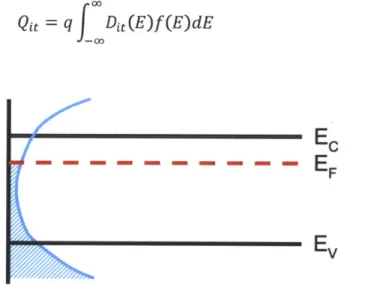
To model the interface states, we can define our own distribution of trap states, Dit, as a function of energy, as shown in Figure 2-9. We can find the total charge accumulated in those traps by integrating across the distribution and accounting for occupation probabilities given by the Fermi-Dirac distribution function. Thus, the charge from interface states can be written as:
= q
J
Dit(E)f(E)dE (43)EC
EF
EV
Figure 2-9 Dit across the energy gap, shown in blue. The filled states are those below the Fermi level.
In actuality, there can be two types of interface states: donor states and acceptor states. Both states are filled as the Fermi level sweeps upwards towards the conduction band. However, acceptor states are neutral until they take an extra electron as they are filled, leaving the states negatively charged as the Fermi level passes through them. This will cause a positive VT shift, relative to a case with no Di,. Conversely, donor states naturally give up an electron, making them positively charged until the Fermi level reaches them and they become neutral. Therefore,
donor states cause a negative VT shift until the Fermi level sweeps through them and they become neutral.
The presence of charge from interface states can be described as a parasitic capacitance that will affect the gate capacitance of the system. The differential capacitance arising from Dit can be written as:
Cj~ - (44)
C't = doQit44
Qit
is the value obtained in (41), and 4jt is the potential at the location of the interface traps. As we will see shortly, 4jt is identical to *s in a surface-channel MOSFET, where the edge of the channel is the semiconductor-oxide interface where the traps occur. With a buried-channel MOSFET, the two potentials are not the same, and we will discuss this in further detail in Section 2.4.3.2.4.2 Surface-Channel MOSFET
The addition of Cit will change the gate capacitance model by adding another capacitance in parallel with the existing Cs and CD, as shown in Figure 2-10. The traps are located at the interface between the channel and the gate oxide.
V ICins
Cs(4S) Ct((s) CD
Figure 2-10 Gate capacitance model for surface-channel MOSFET. Cs, CD, and Cit are as previously defined, and Ci,, is the oxide capacitance.
As mentioned earlier, with a surface-channel MOSFET the channel interfaces directly with the oxide. Therefore, it is clear that ijt should be the same as
4s.
We can write a new expression for the charge on the gate that incorporates the effects of Cit:Os
QG (S) [ s) + + it (s) + CD]ds (45)
This yields a total voltage on the gate of:
CD 1 f's VGS,i = 'Ps + (Ps + - [Cs(Ps) + Cit((Ps)]d)s ins ins 0 (46) 1 = Ps + (qns + PsCD+ QIt) ins 2.4.3 Buried-Channel MOSFET
The presence of a barrier layer between the oxide and the channel can offer various advantages to the performance of a Ill-V MOSFET, and it is for that reason that MOSFETs are often designed with a buried-channel structure such as that in [6]. This separates the interface states from the channel, and helps to reduce scattering. The buried-channel design leads to a gate capacitance model like the one shown in Figure 2-11.
V .L Cins
7it
Cbarrier Os COC it((Oit) Cs(s)T
CDFigure 2-11 Gate capacitance model for buried-channel MOSFET. Capacitances are as previously defined, and Cbarrier is due to the barrier layer between the channel and oxide.
The interface traps manifest in a different location in the buried-channel MOSFET because they always occur at the semiconductor-oxide interface. With the surface-channel MOSFET this happened to be at the surface of the channel, but with the buried-channel design it is at the edge of the barrier and so 4it is no longer the same as *,. Therefore, the derivation of the gate voltage VGSi becomes more complicated. The charge across the barrier layer is equal to the sum, in parallel, of the charge across Cs and CD, and can be found as:
Os
Qbarrier((Ps) = [Cs os) + CD]dJs (47)
If we remember that the charge accumulated in the interface traps is Qit, then the total charge on the gate becomes:
QG (0s,Pit) = Qit Pit) + Qbarrier (0s) (48)
And thus, VGS,i can be written as:
VGS~J = (P +
Qbarrier
QG
(49) Cbarrier Cins which yields: 1 1 VGS,i = (PS + (qn S CD) + (Qi + qn S + s 4sCD) (50) Cbarrier insWe have now developed a methodology for finding the charge from interface states, and accounting for their behavior in both surface-channel and buried-channel MOSFET designs. This, then, completes our considerations for the additions that need to be made to the model in order to accurately describe III-V MOSFET behavior.
2.5 Summary
In this chapter, we have introduced the ballistic transport model for quantum-well FETs that is the basis for a study of experimental data of MOSFETs and HEMTS. We have then extended this model to various first-order effects that will have a significant impact upon the I-V characteristics of this model. We have also discussed theory specific to HEMTs and III-V
MOSFETs in turn. In the following chapters, we will discuss the results of our ballistic transport modeling, and in comparing them against the experimental work, gain insight into the behavior of these FETs and the areas in which we should extend our model further.
CHAPTER 3. SIMULATION RESULTS & EXPERIMENTAL
WORK: HEMT
3.1 Introduction
In this chapter, we use the results of the theory in Chapter 2 to examine the output and transfer characteristics of an experimental HEMT device. We explore first the impact of several key parameters on device characteristics using the simulation environment of Ch. 2. We then compare simulations and experimental data, and detail the process and selection of extrinsic device parameters to best fit the data.
3.2 Device Under Study
The structure of a HEMT was explained in Chapter 1, but we reintroduce the heterostructure in Figure 3-1 so as to specify the choices made by Kim et al. [21], whose experimental data will be the basis upon which we make our comparison. The channel is a 5 nm layer of InAs surrounded by 2 nm and 3 nm In0.53Gao.4 7As cladding layers, and the barrier layer, which is Ino.52A10.48As, is
estimated to be about 4 nm. The gate length is about 30 nm.
-4-~i
Chmnnl 1n053Ga0AAs (2 rn Chaml= 1n0 7Gac As (8 nm) orInAs(5 nm) Channel=IlOMG0OAAS (3 nmn) -8 I Ua--3.3 Simulation Study of Parameters
Before we do a detailed study of our simulation with respect to the experimental device characteristics, it is worthwhile first to take a look at the impact of various parameters on the simulated I-V characteristics. With this understanding, it will be easier for us to both fit the experimental data and to ultimately make meaningful conclusions about any discrepancies.
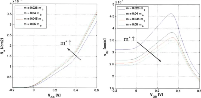
3.3.1 Significance of m*
The main advantage that III-V materials possess over the more traditional silicon is their low-effective mass, leading to increased mobility and therefore the capacity to drive more current. Studies suggest, however, that the effective mass of electrons in the channel of HEMTs and other FETs is larger than that given by the bulk as a consequence of a combination of tensile strain and band non-parabolicity [5]. We must therefore consider the effective mass to be a parameter in the Poisson-Schr6dinger simulations that can be increased to better fit the data and give us a sense for the real effective mass in the channel. The Poisson-Schr6dinger simulations will allow us to account for any increase in the effective mass from the bulk resulting from strain, and we will treat non-parabolicity effects separately in the next section. Here, we explore the effect of varying the effective mass on the sheet carrier concentration, injection velocity, and lastly the transfer characteristics of the HEMT. We will also take a look at the impact of effective mass on the C-V characteristics, but will only consider this in the simulation regime, as experimental data are not available.
From the theory in Chapter 2, we can guess at the influence of effective mass on ns and vinj. We would expect, since n, has a roughly linear dependence on m*, that the sheet carrier concentration will increase as the effective mass increases. We would also expect the opposite effect on the injection velocity, but because vij varies as 1/AV;iF, an anticipated overall increase in current will result. Figure 3-2 shows the results of the simulation in the saturation regime for ns and vinj
for four different effective masses. The InAs bulk value of 0.026 mo is compared to heavier values that are suspected to be closer to the actual experimental value of m* in the channel [5].
We can see that n, rises steadily as VGS increases, with a kink at around VGS = 0.35, and vj also rises steadily until this same point but then dramatically decreases. This is where the device begins to transition from the saturation to the linear regime for high values of VGS, and is caused by nonzero source and drain resistances Rs and RD. More on this behavior will be discussed in Section 3.3.3, where we investigate the impact of the parasitic resistances in detail.
4 X10 5 X10⁷ m = 0.026 m m = 0.026 m 3.5 - m =0.04m 4.5 =0. m =0.046 m m =0.046 m 3 m=0.06 M m =0.06 M 2 .5 ... ... .... ... /. 2R mP" 3.5
m.T
1.5 -1 2.5 0.5 -... 2 -0.2 0 0.2 0.4 0.6 -i.2 0 0.2 0.4 0.6 V Ge IV] V G VFigure 3-2 Effect of m* on n, (left) and vi, (right). Arrows indicate direction of increasing m.
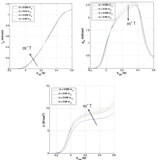
While the general behavior is as predicted by theory-lower vmnj and higher n, for larger m*-the actual impact on transistor characteristics is somewhat more subtle. Figure 3-3 shows the I-V transfer characteristics and gm versus VGs, as well as the C-V characteristics. The value of the m* changes the results of the Poisson-Schr6dinger simulation, in part by affecting how quickly the Fermi level sweeps upwards through the conduction band and the first quantum sub-band, but also by determining in part the location of the sub-bands themselves. The different sheet carrier concentrations with m* also affect the calculation of the gate capacitance as we have described it, which we can see most clearly in the C-V characteristics where the higher effective masses yield a higher capacitance. The sharp rise in the C-V characteristics at high VGS indicate that the second quantum sub-band is beginning to be populated. The overall result, however, is that the total drain current ID does not change much with effective mass. What is more important is the effect on the transconductance gm. The general shape of gm is peaked, where gm increases as the
![Figure 1-1. Schematic of a HEMT structure, reproduced from D. Jin et al. [5]. The red dotted line in the schematic indicates the location of the 6 doping layer, and the channel consists of either](https://thumb-eu.123doks.com/thumbv2/123doknet/14142258.470591/12.918.163.740.680.982/figure-schematic-structure-reproduced-schematic-indicates-location-consists.webp)
![Figure 1-2. Schematic of a MOSFET structure, reproduced from J. Lin et al. [6]](https://thumb-eu.123doks.com/thumbv2/123doknet/14142258.470591/13.918.253.639.580.985/figure-schematic-mosfet-structure-reproduced-j-lin-et.webp)
![Figure 2-4 I-V characteristics of a 30 nm InAs HEMT compared with the HEMT theoretical model, reproduced from [11].](https://thumb-eu.123doks.com/thumbv2/123doknet/14142258.470591/22.918.251.644.408.766/figure-characteristics-inas-hemt-compared-hemt-theoretical-reproduced.webp)