The Arctic Switch Fabric, a Scalable Network
Technology
by
Michael Sy
Submitted to the Department of Electrical Engineering and Computer
Science
in partial fulfillment of the requirements for the degrees of
Bachelor of Science in Computer Science and Engineering
and
Master of Engineering in Electrical Engineering and Computer Science
at the
MASSACHUSETTS INSTITUTE OF TECHNOLOGY
May 1998
(f2 ,@ Michael Sy, MCMXCVIII. All rights reserved.
The author hereby grants to MIT permission to reproduce and
distribute publicly paper and electronic copies of this thesis document
in whole or in part, and to grant others the right to do so.
Author .
...
Department of Electrical Engineering and Computer Science
May 15, 199$
Certified by
...
George Andy Boughton
Prirj4p
Research Scientist
Theur
rvor
Arthur C. Smith
c,-
r
c:
cepolted by
...
JUL14108
Chairman, Department Committee on Graduate Theses
The Arctic Switch Fabric, a Scalable Network Technology
by
Michael Sy
Submitted to the Department of Electrical Engineering and Computer Science on May 15, 1998, in partial fulfillment of the
requirements for the degrees of
Bachelor of Science in Computer Science and Engineering and
Master of Engineering in Electrical Engineering and Computer Science
Abstract
This thesis describes the design and implementation of the Arctic Switch Fabric. The switch fabric will be used to interconnect various SMP's in a fat tree configuration. The task of designing the Arctic Switch Fabric was broken into designing a Four Leaf Board and a backplane to which multiple Four Leaf Boards may be connected.
The design and implementation phase of the Four Leaf Board and the backplane entailed the generation of digital circuits that met the project specifications, writing behavioral models of the selected parts in Verilog, and verifying the behavior of the complete circuit. After verifying the design, a corresponding netlist in Allegro format with parts information was sent out for PC Board layout and manufacturing.
Most of the original objectives have been met. The first Four Leaf Board has been assembled and is in service. The PC Board for the backplane has been fabricated and will be assembled shortly.
Thesis Supervisor: George Andy Boughton Title: Principal Research Scientist
Acknowledgments
I would like to thank all the individuals and organizations that made this journey possible.
First, I would like to thank my thesis supervisor, Dr. George Andy Boughton. It has been a privilege to work under his guidance and support for the past year. He has been a constant source of inspiration and advice that has been immensely helpful in the completion of this thesis. Thanks Boss!
I am also grateful to the Computational Structures Group in MIT-LCS headed by Prof. Arvind for the opportunity to do research in his group. It has been a great learning process for me to be working in within a group of sharp computer architecture people.
Thanks also go out to Chiangkai Er, Geoff Lee Seyon, Weiyang Cheong, Choonsiang Tan, Tammy Yap, Cheewe Ng, Kokkeong Puah, Xuanhui Ng, Tommy Ng, Ben Leong, Tracey Ho, Steven Lee, and Tseh-hwan Yong who have made my stay at MIT a very memorable and pleasant one.
Finally, special thanks go to my parents, Manuel and Maria Sy; my brother, Manchester; my sisters, Marilyn, Marivic and Marianne; and Ellice Siytiu for their unending support, love and care throughout the course of my education at MIT.
_ ~_~~~___...lr-- -c-~ ^-~Y~-- C--- y
Contents
1 Introduction
1.1 Problem Statement and Motivation . . . . . 1.2 Arctic Switch Fabric . . . . 1.3 Four Leaf Board ...
1.4 Arctic Routing Chip . . . . 1.5 StarT . . . .
1.5.1 StarT-Voyager ... 1.5.2 StarT-X . ...
2 The Four Leaf Board
2.1 Functions and Design Issues . . . . 2.1.1 Arctic Chips . . . . 2.1.2 ECL-GTL Conversion Circuitry . . . 2.1.3 Retiming Circuitry . . . . 2.1.4 JTAG and Clock Distribution . . . .
2.1.5 Connectors and Links . . . . 2.2 Implementation . . . .
3 The Backplane
3.1 Functions and Design Issues ... 3.1.1 Connectors and Routing .. . 3.1.2 JTAG Distribution ... 3.1.3 Clocks ... 15 15 15 16 17 18 20 22 23 . . . . . 25 . . . . 25 . . . . 27 . . . . 29
3.1.4 Power Taps ... ... .... 30 3.2 Im plem entation ... 31 4 Status Report 32 4.1 Current Status . .. ... . .. .. . .. .. . .. .. . ... .. . .. 32 4.2 Further W ork ... ... ... 33 4.3 Accomplishments ... 34 _IP---I-~I~
-List of Figures
1-1 The Arctic Switch Fabric . . . . 1-2 Fat Tree Structure of the Arctic Switch Fabric . 1-3 Block Diagram for the Scalable Four Leaf Board 1-4 Arctic Block Diagram ...
2-1 GTL-ECL conversion . . . . . 2-2 JTAG circuitry . . . . 2-3 Clock Distribution PLL . . . 2-4 Clock Pads . . . ..
3-1 Floor Plan for the Backplane 3-2 Layer 1 Routing . . . . 3-3 Layer 2 Routing . . . .. 3-4 Layer 3 Routing . . . . 3-5 Layer 4 Routing . . . . 3-6 Pin to Pin Routing . . . . 3-7 Backplane JTAG distribution 3-8 Backplane Clock Circuitry . .
~...~~~
-
Y~ -U--~-
---
--
YL
p---
.
.
.
Chapter 1
Introduction
1.1
Problem Statement and Motivation
This thesis aims to design and implement the Arctic Switch Fabric, a scalable network technology that will be used to route packets in the StarT project. There are two main design challenges in this project. One is to design the Four Leaf Board which will serve as the basic unit of the switch fabric, and another is to design the backplane which will connect each of the Four Leaf Boards together.
The original idea for the Arctic Switch Fabric was conceived to support the StarT project. The StarT is a project aimed at developing a general purpose parallel sys-tem based on scalable architectures, implicitly parallel programming languages, and explicitly parallel dialects of conventional programming languages. Hence, to support scalable architectures, the Arctic Switch Fabric project was undertaken.
The Arctic Switch Fabric will be based on the Arctic Routing Chip that was designed in MIT. A brief description of the Arctic Switch Fabric, the Four Leaf Board, and the Arctic Routing Chip can be found in sections 1.2, 1.3, and 1.4 respectively. The StarT project is also briefly described in section 1.5.
The design of the Four Leaf Board can be found in chapter 2, while the design of the backplane can be found in chapter 3.
1.2
Arctic Switch Fabric
The Arctic Switch Fabric is designed mostly from off the shelf parts except for the Arctic Routing Chip [3] which was designed in MIT. It provides a 308Mbyte/sec/full-duplex-link with differential ECL signalling on the leaf nodes.
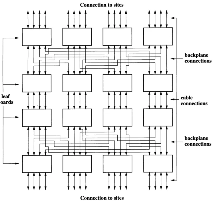
As shown in Figure 1-1, the switch fabric consists of a backplane, a few four leaf fat tree boards and a JTAG host. The current design has 16 four leaf fat tree boards per card cage which will result in a 32 leaf fat tree network. The card cages can in turn be connected to other card cages to result in larger networks.
tree
Backplane
Figure 1-1: The Arctic Switch Fabric
The switch fabric has a fat tree [5] structure as shown in figure 1-2. Although it is programmable which will allow it to be used in some other applications of staged networks. To program the switch fabric, the JTAG host is used.
Aside from programming the Arctics, the JTAG host also keeps track of statistics related to the network. Some of the statistics it keeps are error counts, and packet counts.
Connection to sites backplane connections cable connections backplane connections Connection to sites
Figure 1-2: Fat Tree Structure of the Arctic Switch Fabric
4 leaf
boards
_ .~---I1I I-_---L I~1I-~I.- ---~ ..l.-- -^l -~l-C .-I__._ I-.II~-1II I~-rr~CIL1- ~_
1.3
Four Leaf Board
The block diagram for the Four Leaf Board is shown in figure 1-3. It consists of four Arctic chips (AO, Al, A2 and A3); GTL-ECL and ECL-GTL conversion and retiming circuitries; clock distribution circuitry; JTAG circuitry; cable connectors;
and backplane connectors.
The voltage conversion circuitries are needed to translate the signals coming in from the network, which are in ECL, into the switch fabric, which communicates in GTL. After conversion, the packets are routed within the switch fabric in GTL until they are transmitted back out, in which case they will be converted into ECL signals. Due to skew effects of might arise in the transmission and voltage conversion of the signals, retiming was done. The retiming circuit was also responsible for rescaling the clock frequency that is sent with the data. Although the data rate for the incoming and outgoing data are the same, the Arctic Chip clocks its internal data differently from the incoming and outgoing data. The incoming and outgoing data to and from the nodes are clocked at 77MHz using the rising edge of the clock, while the internal data in the Arctic Chips are clocked at 38.5MHz using both edges of the clock.
The clock distribution is used for two purposes. One is to buffer and clean the clock signal coming in from the backplane to the Arctics, so as to ensure a clean clock signal with acceptable duty cycles. Another is to control the phase relationships of the clocks going into the four Arctics as needed.
The Four Leaf Board as a whole provides eight full-duplex links. Four of these can be connected externally by cables, either to an SMP or to another part of the network. While the other four are connected to the backplane and form the structure shown in figure 1-2.
1.4
Arctic Routing Chip
The Arctic Routing Chip was developed for use in the StarT project. The chip is a four input, four output packet switched router that can be used to implement a
Figure 1-3: Block Diagram for the Scalable Four Leaf Board
11
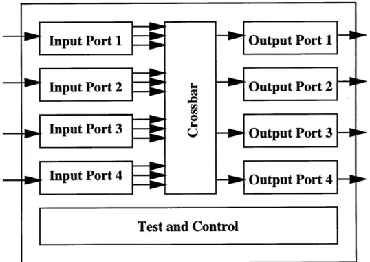
-I1IL-variety of staged networks. It is capable of supporting two packet priority levels, with packet sizes of up to 96 bytes. It also has an extensive error detection, but limited error handling mechanism; and is able to keep statistics. Although it is designed for use in fat tree networks, the chip can be reconfigured through the JTAG port for use in different staged networks.
The basic structure of Arctic is shown in Figure 1-4. It basically has 4 major sections. The input section, the output section, the crossbar and the test and control section. Each input section has its own clock domain, while the crossbar and the output section has another which results in a total of five different clock domains for each Arctic chip.
Input Port 1
Input Por
t2
Input Port 3
Input Port 4
k, 9 USOutput Port 1
Output Port 2
-
Output Port 3 -1
Output Port 4
Test and Control
Figure 1-4: Arctic Block Diagram
The routing of a packet in Arctic is determined by the packet header which is attached by the source. The first half of the header determines the up-route of the packet while the second part of the header determines the down-route.
1.5
StarT
The StarT project is aimed at developing a general-purpose parallel systems based on scalable architectures, implicitly parallel programming languages, and explicitly parallel dialects of conventional programming languages. Two of the undertakings in the project which will be using the Arctic Switch Fabric are presented in the following sections.
1.5.1
StarT-Voyager
The StarT-Voyager [1] [2] is a project that aims to build a high performance, flexi-ble message passing and coherent shared memory parallel machine using commercial SMP's. To connect the SMP's together, one processor in each SMP is replaced by a Network Endpoint System (NES) adapter card which is in turn connected to the Arctic Switch Fabric.
For the end nodes of this network, PowerPC 604E dual processor SMP will be used. The NES, which acts as the network interface, replaces one of the processors in the SMP and plugs in directly to the memory bus of the system. The NES board thus handles the interaction of the SMP site and the network and assures cache coherency. It supports four different types of messages to efficiently handle a wide variety of communication needs.
The NES contains an embedded processor which can be programmed to support other cache coherency and message passing protocols as desired. This is done to facilitate the study of the performance of different protocols on parallel machines.
1.5.2
StarT-X
The StarT-X [4] project aims to build a high performance parallel machine with support for message passing. The difference between the StarT-Voyager and StarT-X is that the StarT-X project will be connected to the Arctic Switch Fabric with a Network Interface Unit (NIU) card instead of the NES.
L~ --.- .IS--~~ ~--F-liCILIP E(IIYDYP~I~~~-Y~-Yllllsl~
Instead of connecting the SMP's through their memory bus, the NIU connects to the PCI bus of the SMP and is thus able to support a wider class of machines. This is because the PCI bus is a standard communication protocol as opposed to the vendor specific memory bus. Although the approach of using the PCI bus instead of the memory bus sacrifices some performance, like not being able to implement more aggressive cache coherency protocols, it is able to support a wider variety of SMP's and can conceivably adapt to emerging technologies.
Another difference between the NES and NIU is that the NIU is fully implemented in hardware. This makes the NIU non-programmable as opposed to the NES which makes it less flexible.
The StarT-X supports two different priorities of messages and three different modes of message passing. These modes are direct memory mapped register interface; message passing queues through host DRAM; and DMA transfer.
Chapter 2
The Four Leaf Board
The basic unit in the Arctic Switch Fabric is the Four Leaf Board. As shown in Fig-ure 1-3, it has 8 full-duplex links. Four of these links are connected to the backplane and the other four are connected to the network. It also has four Arctic chips for routing packets, ECL-GTL conversion, retiming, JTAG distribution and clock dis-tribution circuitries. The function .and design issues related to each of these parts will be discussed in section 2.1. The board also contains some passive elements, like resistors and capacitors, to ensure proper functionality.
In the implementation phase, the code corresponding to the design was placed into Verilog and then tested on the software level. After which, the code was then used to generate a netlist in Allegro format that was sent to a third party for PCB layout and manufacturing. The work entailed for this process is described in more detail in section 2.2.
2.1
Functions and Design Issues
2.1.1
Arctic Chips
All the packet routing within the switch fabric is done by the Arctic Chips. They also keeps track of statistics such as error counts and packet counts. Although the Arctic chip does not do error correction, it does some error detection as it performs
CRC on both the incoming and outgoing packets.
The interconnection of the four Arctic Chips on the Four Leaf Board is shown in Figure 1-3. This configuration is due to the fat tree structure of the switch fabric. As shown in figure 1-2, the fat tree configuration of the switch fabric is obtained by connecting the Four Leaf boards through a backplane.
2.1.2
ECL-GTL Conversion Circuitry
The ECL-GTL conversion circuitry is needed because the nodes of the network and the Arctic chips communicate using two different voltage levels. The incoming data use Emitter Coupled Logic (ECL), while the Arctic Chips uses Gunning Transceiver Logic (GTL) to pass bits of information along.
ECL dissipates more power than TTL but has a small voltage swing. The op-erating voltage of ECL is about 3.2 volts to 4.1 volts. On the other hand, GTL provides high speed, backplane and point-to-point communications with lower dissi-pation. The operating voltage for GTL is from 0.2 volts to 1.2 volts. The reason for using differential ECL for the incoming data is to have more noise tolerance on the data. This is needed since the data are passed along using cable from the nodes to the switch fabric. Single ended GTL was sufficient for Arctic to Arctic communication since it happens in a shielded environment inside the switch fabric.
The design for the conversion circuitry was taken from the board which was built by Dr. Andy Boughton to test the first few Arctic chips. In this implementation the outgoing GTL signal from the Arctic chips were passed through a voltage divider as shown in Figure 2-1 that basically increased the voltage level of the GTL signals. This signals were then passed on to an ECL buffer which had a large common mode input tolerance that worked with the range of voltages coming out of the voltage divider. These outputs were then registered and passed on to the nodes as ECL signals.
On the other hand, the incoming ECL signals from the nodes to the Arctic chips were first passed though an ECL to TTL converter and then passed through a voltage divider to obtain a GTL signal. The reason for this is that it is hard to achieve a valid logic low conversion from an ECL signal (3.2-3.5 volts) to a valid zero GTL
ECL Signal
ARCTIC ECL Buffer
GTL Signal
Figure 2-1: GTL-ECL conversion
signal (0.2-0.8 volts) by using a voltage divider and still maintain a valid logic high conversion. The availability of a commercially produced ECL-to-TTL converter like the 100ELT23 was helpful in this case.
2.1.3
Retiming Circuitry
Due to possible signal skew that might arise from transmission delays and voltage conversion, a retiming circuit was needed. The retiming circuit also rescales the clock frequency since the incoming and outgoing data, from and to the nodes, are clocked using the rising edge of a 77MHz clock while the Arctic Chips uses both edges of a a 38.5MHz clock for handling internal data. The retiming circuit that was used here is also based in part on the board designed to test the first few Arctic Chips.
The frequency of the incoming data clock is halved using a D flip-flop and the resulting clock is used by the Arctic to clock its internal data bus. To ensure that there is no loss of data, the incoming data, which is 16 bits, is registered inside the
Arctic which has a 32 bit internal data bus.
For the outgoing clock, a doubling in clock frequency is achieved by using a phase locked loop (PLL). This clock is then used at the output registers to time the outgoing data from the switch fabric to the nodes.
One minor revision from the design used in the testing of the Arctic Chip was the use of the Synergy 89421V PLL. On the board that was used to test the Arctic
Chips, they used a semi-custom PLL to double the frequency of the clock as there were no commercially available PLL in the market that met specifications. However
during the design of the Four Leaf Board, the Synergy 89421V PLL was already available and thus it was used in favor of the semi-custom chip. Even though the semi-custom PLL had a better specification, the Synergy 89421V was used since it was more economical.
2.1.4
JTAG and Clock Distribution
The JTAG and clock distribution circuitry for this board was designed to meet a few requirements. For the JTAG, since it is used for programming the Arctics and looking at statistics, the board should be able to get signals from the backplane, access all the Arctics and then go back out to the backplane. This is achieved by a circuit as shown in Figure 2-2.
For this implementation, the clock, mode select and reset are buffered signals so all the four Arctics see the same signals. For the data in and data out, it is implemented as a serial input that is passed along through the four Arctics and results are sent back out as a serial output. Although this implementation could be made faster by making the Arctics individually programmable by using a dedicated path from the JTAG host to Arctic, this will result in a higher pin count going into the board.
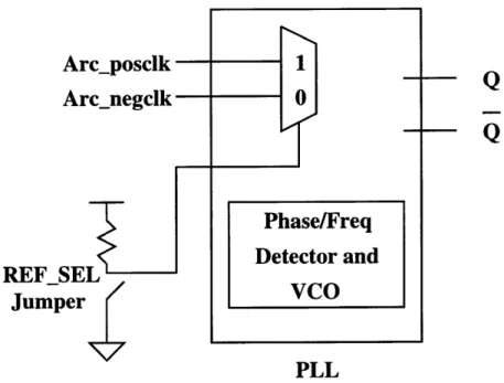
The clock distribution circuit for this board serves two purposes. One is to buffer the clock signals coming in from the backplane to the Arctics to ensure clean clock signals with acceptable duty cycle. Another purpose of this circuit is to control the phase relationship of the clocks going into the Arctics as needed. To be able to clean the signal and at the same time control the phase relationship of the clock, a PLL was used. The block diagram of the PLL used, along with some support circuitries, is shown in Figure 2-3.
The problem of controlling the phase relationships of the clock was discovered while testing the first few Arctic chips that were manufactured. Originally, the Arctics were designed to be totally asynchronous, which would have eliminated the problem of phase relationships. Unfortunately, a flaw in the synchronizer circuit of the
Mode Select (TMS)
Clock (TCLK)
Figure 2-2: JTAG circuitry
tic dictates that communicating Arctics be run synchronously within certain phase constraints.
The phase relationship problem was that the rising edges of the clocks going into communicating Arctics could not be too close to one another. To prevent the rising clock edges of communicating Arctics to be too close to one another, clocks were routed to Arctics such that alternating stages, in the fat tree configuration, received
clock and clock. Since a Four Leaf Board contained 4 Arctics which are basically
part of 2 stages in the fat tree configuration, the
Q
andQ
of the PLL were routed to each stage. On the other hand, controlling the phase relationship of communicating Arctics on separate Four Leaf Boards is done by appropriately setting the REFSELi~.rr.c.r^-..r*- -rYr~-r;Lu^~C~ ~~pu~~~- L4~. --- ---i--- -I-rrr-ir~---~--~----_-- ---~-rrrrmrruzr 1
Arc_negclk
0
Q
Phase/Freq
Detector and
REFSEL
Jumper
VCO
PLL
Figure 2-3: Clock Distribution PLL
input of the PLL, which is a hardware jumper, to select whether the positive or negative global clock should be used.
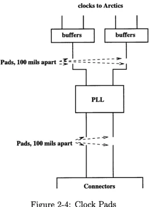
For the Four Leaf Board a mechanism to further control the phase relationships of the clock was added. This is shown in Figure 2-4. Basically, the wire traces of the incoming clocks from the backplane, and the wire traces of the clocks being fed to the PLL were not connected but were rather made to be exposed contacts 100 mils apart on the board. This allowed the addition of wire delays on the clock, as needed, by inserting long wires in between the two exposed pads. Additional clock pads were also inserted between the PLL and the clock buffers for the Arctics.
To reduce noise on the clock links that might have been produced by having exposed pads, the clock signals were run close to ground signals. Hopefully, wire delays will not be needed to control the phase relationships of the clock which will allow the removal of the exposed pads from future versions of the board.
2.1.5
Connectors and Links
There were two different types of connectors used on the Four Leaf Board. One type was a 100 pin cable connector which was used to send ECL signals from the nodes
~__CII ~_____li_~ _I__ 1^ ~_1~-~^1_~*- -~ 11111-~ ~---1 -1~1~--- llse_
clocks to Arctics
Pads, 100 mils apart t f= -
-PLL
Pads, 100 mils apart --- - -
--Connectors
Figure 2-4: Clock Pads
to the board. Each board had four of these cable connectors, one for each external link. Since each link was a full-duplex, differential ECL link, there were a total of 80 signals being passed which needed 80 pins. These signals were comprised of 64 signal data for the 16 bit incoming and outgoing data, 8 for clock signals, and 4 signal bits each for the frame and buffer signals. The rest of the pins were connected to ground to establish a common ground and lessen noise on the transmission.
The other connector used was a 160 pin micro-strip right-angle connector. Two of these were used per board with two links per connector. The signals that were being passed here were single ended GTL signals so there were 40 signals per link for a total of 80 signals but there were also JTAG signals, clock signals and power connections from the backplanes.
The JTAG signals from the backplane take up 5 pins from the connector and the clock take up another 2 while the rest are used for power distribution. The power connections were done in proportion to the amount of current that the board was estimated to need at each voltage level source. The ratio between the current needs of VDD (5V), VTT (3V) and VGT (2V) approximately 3:1:1.
2.2
Implementation
To implement the Four Leaf Board, a software model was first written up and verified in Verilog, with both the chips and passive devices included, then the code was used to generate a netlist in Allegro format that was sent to a third party for PC board layout and manufacturing. The generation of the Verilog code entailed writing up behavioral models for some of the chips and then testing them both as a unit and as a part of the whole system. Since the timing constraints of the board were taken cared of by link specifications (ie. length of wires), which will be done in the PCB layout, only functionality and proper connectivity of the wires were checked without emphasis on timing.
In simulating the whole board, a few simplifications were done. One major sim-plification was that the Arctic chip was modeled as a buffer. This is possible because the Arctic is known to work from both software and hardware tests in its production. A full Arctic model would only hamper the simulation time of the Four Leaf Board.
The simulation helped in detecting and fixing connection errors that were made in the first few iterations of the software model. One thing the simulation did not do was test the behavior of the passive devices such as capacitors and resistors. Hence, to make sure that the passive devices were in the right place, for termination and proper PLL functionality, emacs macros were used verify that they were placed appropriately. After simulation, a script was used to generate an Allegro format netlist from the Verilog code. This process entailed writing a mapping of every component in the design to instance names that would appear on the PC board. The resulting Allegro netlist, along with parts information, was sent to a third party for PC board layout and manufacturing.
Chapter 3
The Backplane
The backplane will serve to interconnect the Four Leaf Boards together in a fat tree configuration. Each backplane will be able to contain up to 16 Four Leaf Boards that will provide support for up to 32 nodes. The backplane has connectors, JTAG distribution circuitries, clock circuitries which provide a central clock and distribution channel for the Four Leaf Boards, and power taps. The functions and design issues related with each of these parts will be discussed in the next section. The backplane also contains some passive elements, like resistors and capacitors, to ensure proper functionality.
As done with the Four Leaf Board, the implementation of this backplane was first done by coming up with a software model for the design and test. After this, it was used to generate a netlist in Allegro format and sent out for PCB layout and manufacturing.
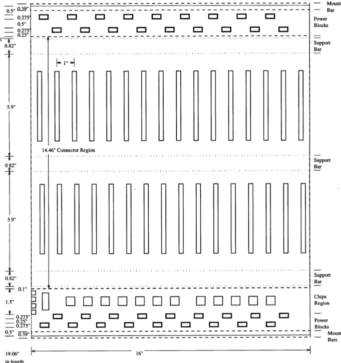
A floor plan of the backplane that shows the location of each component, along with the mounting bars and support bars, is shown in Figure 3-1.
I_ _ ( II __1__~~_1_ ~ II C I--. ^~ l L--.. ll^l IIIIY ~IIII (I~ PI-- Ill-_-~-yrm*l-- - ~
- --- --- ---- ---.039" - --- --0.2755" 0.5" 0.275' 0.25" 0.182"
"
1 14.46" Connector Region- - -14.46" Connector Region 5.9"--
i--0 82" 0.1" - - - -0.275" 0000 0.275" 1 -' 1 I " [ ' ' ' ' 0.25" 0.5'_2' b--19, L 19.06" in lengthFigure 3-1: Floor Plan for the Backplane
- Mount - Bar Power Blocks Support Bar Support Bar Support Bar Chips Region Power Blocks Mount Bars I ^^__ ---
L-0
2"
3.1
Functions and Design Issues
3.1.1
Connectors and Routing
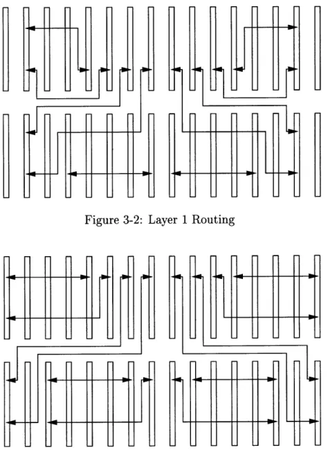
To connect the Four Leaf Boards to the backplane, the backplane has 32 160 pin micro strip connectors. These connectors can be divided into two sets of 16, one set on the right side of the board and one on the left, and routed in four signal layers as shown in Figures 3-2, 3-3, 3-4, and 3-5. Each line from a connector to another is a set of 40 traces.
1f-r ri 1 ri
Figure 3-2: Layer 1 Routing
Figure 3-3: Layer 2 Routing
Figure 3-4: Layer 3 Routing
Figure 3-5: Layer 4 Routing
The connector to connector routing, shown in Figures 3-2 to 3-5, were designed to minimize the number of signal layers used. On the other hand, the pin to pin rout-ing was done by choosrout-ing pin assignments carefully to make the wirrout-ing connections uniform.
The upper half of the connector and its pin to pin routing is shown in Figure 3-6. The pins marked P are power pins, those marked G are ground pins, while those marked T and R are transmitter and receiver pins. The P and G pins are direct connections to the power planes while the T and R pins were chosen such that the routing shown in Figure 3-6 is possible. The left and right side of Figure 3-6 shows
how each trace is connected from the pin to pin and the middle column shown how traces are routed in between pins if there are no connections to be made to a certain connector.
There are two connectors for each Four Leaf Board and the bottom half of the connectors, which are not shown in Figure 3-6, differ with each other. The bottom half of the bottom connector has the same routing as shown in the figure but the bottom half of the top connector has 7 power pins used for JTAG connections and clocks. The signals which uses these pins are the JTAG clock, JTAG data in and data out, JTAG reset, JTAG mode select, and the positive and negative Arctic clocks.
3.1.2
JTAG Distribution
The JTAG circuit takes its input from an external source, the JTAG host, and delivers its output back to the host. The input from the host is then distributed to the Four
Leaf Boards through the circuit shown in Figure 3-7
As shown in the figure, the JTAG host is connected to the backplane through a cable connector. The connector is a 16 pin cable connector, of which 5 pins are signal pins and the rest are ground pins to help reduce the effects of noise during transmission. The JTAG data in (TDI) and data out (TDO) creates a big ring that
goes all the way around all the Four Leaf Boards, and effectively all around the Arctic Chips, and goes back out to the host. This provides the host with a way to send data to and receive data from each Arctic in the switch fabric.
The JTAG mode select (TMS), reset (TRST), and clock (TCLK) are just buffered directly to the Four Leaf Board using 1-to-10 buffers. The 8 boards on the left side of the backplane gets the same signals, plus or minus some chip and transmission skew, and similarly, the 8 boards on the right side the board gets the same signal. With this buffering scheme, the signals seen by a Four Leaf Board goes through the same number delay elements and should preserve the phase relationships of TMS, TRST, and TCLK as much as possible.
-O
0
@
0-
-
®
,
__
O.L.___
0
@0-
-0
@
00-
0-00
0@
0-G
0
00-
@
0-0
0--o
@
Figure 3-6: Pin to Pin Routing
Cable Connector to/from JTAG host
Figure 3-7: Backplane JTAG distribution
3.1.3
Clocks
To support scalability of the Arctic Switch Fabric to more than 32 nodes, stacking of multiple Arctic Switch card cages had to be supported. To be able to support the communication of multiple card cages, a central clocking mechanism was needed to control the phase relationship of the clocks going to each Arctic. The capability of supplying and receiving a central clock was thus placed on the backplane.
The circuit shown in Figure 3-8 allows the backplane to supply the Four Leaf Boards directly connected to it with a clock that either comes from an on-board oscillator, or from the network. To be able to select from the two clocks, a dual input PLL with input selector, just as in the Four Leaf Board, was used.
In the case that only one switch fabric is being used, the local oscillator will be used to clock the Four Leaf Boards and the INPLLSEL input of the PLL will be set appropriately. The clock signals will then be buffered from the PLL using a four 1:10 buffer that will go to the Four Leaf Boards. On the other hand, if multiple card cages are being stacked together, the backplane can either supply a global clock to other card cages or receive and buffer the global clock which comes from the network.
The net_clockin input in Figure 3-8 is an external input coming from the network which corresponds to the global clock, if and when the card cages are stacked together.
---n-lrxr~y~r~r~-~ lIl---r~L--i~-CiYY
Net_clockout (3) Positive Arctic clocks to Four Leaf Board n _ 8 Negative Arctic Q0 clocks to Four SLeaf Board 1 Q
Oscillator 8 Positive Arctic
Q clocks to Four Leaf Board
Detector and
Detector and 8 Negative Arctic
INPLLSEL VCO clocks to Four
Leaf Board
PLL 1:10 Buffers
Figure 3-8: Backplane Clock Circuitry
To use this the INPLL_SEL is connected to ground by using a hardware jumper and this clock will then be buffered to the Four Leaf Boards. If there is a need to buffer this global clock signal to other card cages, it can be done by connecting the net_clockout outputs, as shown in the figure, to the other card cages. However, if the card cage is the one supplying the stacked network of card cages with the global clock, the oscillator input will be selected and the net_clockout outputs will be connected to other card cages.
3.1.4
Power Taps
The Arctic Switch Fabric has a power supply that provides all four voltages levels (VCC, VGT, VTT and GND) needed in its operation. To connect the power supply source to the backplane, power taps were used. The power taps used were rated at
25 amps carrying capability.
From testing the first few Arctic Chips, it was estimated that the components of a Four Leaf Board need about 15 amps of VCC current, about 5 amps of VTT current, and about 5 amps of VGT current. To meet these current requirements, 36 power taps were used. Four of these power taps were used for VGT, four for VTT, 14 for VCC and another 14 for GND.
The power taps were distributed around the board as shown in Figure 3-1. The power taps were split between the top and bottom part of the board, each of them having 7 taps for VCC, 7 taps for GND, and 2 taps each for VGT and VTT. The distribution of the power taps on the backplane were done such that both the top and bottom parts had VCC, VGT, VTT, and GND to ensure that current sources on
the board were distributed.
3.2
Implementation
As with the Four Leaf Board, a model for the backplane was first written up and verified in Verilog. After verifying that the model was functioning properly, the code was used to generate a netlist in Allegro format which was sent to a third party for PCB layout and manufacturing.
The code generation for the software model entailed writing up some behavioral models for the chips that were used and then testing each of them individually and as a part of the whole backplane. To test the software model, simulations were done. Similar to the Four Leaf Board, it was hard to test for passive elements that were used in the backplane, so emacs macros were used to verify their placement.
After verification, a script was used to generate a netlist in Allegro format from the Verilog code. This process entailed writing a mapping of every component in the design to instance names that would appear on the PC board. The resulting Allegro netlist, along with parts information, was then sent to a third party for PC board layout and manufacturing.
Chapter 4
Status Report
4.1
Current Status
The PC board for the Four Leaf Board has been manufactured and populated with chips. To date, the board has been tested in hardware for approximately two months. The board has so far exhibited proper functionality through the testing. period by routing packets between four PC's using the StarT-X NIU board. Since the first Four Leaf Board is functional, more boards are now being procured for testing with the backplane.
The PC board for the backplane has been laid out and manufactured but it has yet to be populated with chips. The delay is due to problems in obtaining the low skew 1:10 buffers that were used in the design. The design was done thinking that these chips were available in LCC packages but it turns out that the manufacturer has stopped supporting this package. Current options under consideration include obtaining programmable chips in 20 pin LCC packages to act as a replacement or using adapters to convert available buffers to a 20 pin LCC footprint.
The card cage, which will serve as the enclosure for the Switch Fabric, is being worked on with the cooperation of a third party manufacturer. The card cage will house the backplane, the Four Leaf Boards, and possibly the power supply.
4.2
Further Work
As the PC board for the backplane has not yet been assembled, the testing of the backplane, both by itself and with the Four Leaf Board, has yet to be done. This testing will be done as soon as the board has been assembled.
Another matter that needs to be done is to settle the engineering details associated with the the card cage. The engineering details regarding mounting bars, support bars, power supply placement, and cooling apparatus are still being decided upon.
Testing of the whole Arctic Switch Fabric in conjunction with the StarT-Voyager and StarT-X system should also be done. Specifically, the test should check for the interfacing of the NES and NIU boards, which will be used with the StarT-Voyager and StarT-X project respectively, with the switch fabric.
The current design of the Four Leaf Board and the backplane consumes quite a lot of power. Although it has been a learning process to make sure that the all the links are properly terminated and to make sure that noises are attenuated, the design is nowhere near optimal in terms of power consumption. Some details which may be worked on in the future include the amount of capacitance that is actually needed for the boards and whether the termination resistors can be changed in some links to optimize power consumption.
The current design of the backplane requires that the backplane be fully populated with 16 Four Leaf Boards for the JTAG host to perform all its functions. This is because the JTAG routing is done in such a way that all the Four Leaf Boards form a big loop with the JTAG host. One possible improvement will be for the JTAG host to still perform all its functions without the backplane being fully populated with
Four Leaf Boards.
Another possible future improvement is to provide support for a central JTAG host when card cages are stacked together to support more than 32 nodes. What this will provide is the ease of managing all the card cages and also ease of programming.
4.3
Accomplishments
This thesis set out to design and implement the Arctic Switch Fabric. Specifically, the task was to design and test the Four Leaf Board, which will be the the basic unit of the switch fabric, and the backplane, which will serve to interconnect the Four Leaf Boards in a fat tree structure that supports 32 nodes.
Most of the original project goals have been achieved. Both the Four Leaf Board and the backplane have been successfully designed and tested on the software level. So far, the hardware testing for the Four Leaf Board has been very satisfactory as it has been able to successfully route packets from four PC's using the StarT-X NIU board. The PC board for the backplane has been fabricated and will be tested shortly.
Bibliography
[1] Boon S. Ang and Derek Chiou. StarT-Voyager. In The Proceedings of the MIT
Student Workshop for Scalable Computing, 1996.
[2] Boon S. Ang, Derek Chiou, Larry Rudolph, and Arvind. Message Passing Sup-port in StarT-Voyager. Technical reSup-port, Massachusetts Intitute of Technology, Computation Structures Group Memo 387, July 1996.
[3] G.A. Boughton. Arctic Routing Chip. In Proceedings of Hot Interconnects II, August 1994.
[4] James Hoe. StarT-X: A PCI Arctic Network Interface Unit. In Internal Memo
found in http://www.csg.lcs.mit.edu:8001/StarT-X/overview.html, 1997.
[5] C. E. Leiserson. Fat-Trees: Universal Networks for Hardware-efficient Supercom-puting. In IEEE Transactions on Computers, pages C-34(10), October 1985.