Breaking the bottleneck in radiation materials science with transient
grating spectroscopy
by
Sara Elizabeth Ferry
Dual B. S., Nuclear Science and Engineering and Physics (2011) Massachusetts Institute of Technology, Cambridge
S. M., Nuclear Science and Engineering (2016) Massachusetts Institute of Technology, Cambridge
SUBMITTED TO THE DEPARTMENT OF NUCLEAR SCIENCE AND ENGINEERING IN PARTIAL FULFILLMENT OF THE REQUIREMENTS FOR THE DEGREE OF
DOCTOR OF PHILOSOPHY IN NUCLEAR SCIENCE AND ENGINEERING AT THE
MASSACHUSETTS INSTITUTE OF TECHNOLOGY
JUNE 2018
©Massachusetts Institute of Technology All rights reserved
Signature of author:
Sara Elizabeth Ferry
Department of Nuclear Science and Engineering May 17, 2018
Certified by:
Michael Short
Norman Rasmussen Assistant Professor of Nuclear Science and Engineering Thesis Supervisor
Certified by:
Ju Li
Battelle Energy Alliance Professor of Nuclear Science and Engineering Professor of Materials Science and Engineering Thesis Reader
Certified by:
Michael Demkowicz
Associate Professor of Materials Science and Engineering, Texas A&M University Thesis Committee Member
Accepted by:
Ju Li
Breaking the bottleneck in radiation materials science with transient grating spectroscopy Sara E. Ferry
Submitted to the Department of Nuclear Science and Engineering on May 17, 2018 in Partial Fulfillment of the Requirements for the Degree of Doctor of Science in Nuclear Science and Engineering
Nuclear power applications are characterized by harsh mechanical, chemical, thermal, and irradiation environments that present a challenge for the materials engineer. Nuclear materials research and develop-ment is a subject of managing constraints: a component must be proven to retain its integrity in the reactor environment for the entirety its operating lifetime, and the material must not impede the delicate neutronics balance that makes a reactor work.
It is not surprising, then, that materials often represent the major engineering hurdle in moving a new reactor concept closer to reality, especially since many advanced reactor concepts utilize higher temperature regimes, larger radiation fluxes, and more corrosive coolants. However, if nuclear materials research is the bridge between academic concept and commercial reality, it is frequently a long and expensive bridge to cross. In order to validate a new material for use in a specific reactor environment, one must test the material in representative conditions, or test the material in a sufficient number of conditions that the material’s response to an arbitrary reactor environment can be accurately predicted.
Transient grating spectroscopy (TGS), long used in the materials science field to characterize the proper-ties of thin films, is adapted for use as a method of characterizing radiation-damaged samples. TGS has the ability to simultaneously measure elastic, thermal, and acoustic material properties. It is also non-contact and non-destructive, and relatively inexpensive to build and adapt for different uses. This means it is an ideal candidate for moving the field of nuclear materials closer to the goal of having the ability to fully character-ize the radiation-induced property changes in samples in situ and in real-time while they are irradiated. This thesis demonstrates, via a TGS setup built in the MIT Mesoscale Nuclear Materials laboratory, that TGS will be a valid method for quantifying radiation damage by using it to characterize (1) cold-worked irradiated samples, (2) samples with high concentrations of constitutional vacancies, and (3) samples irradiated for 14 years in the EBR-II reactor.
In (1), it is shown that TGS is a viable method for measuring thermal diffusivity changes due to radiation damage at low doses in cold-worked single crystal niobium. In particular, an initial decrease in thermal diffusivity at very low doses is measured, which is attributed to electron scattering by point defects, followed by an increase and saturation of thermal diffusivity as dose increases, which is attributed to less efficient electron scattering as point defects cluster into mesoscale defects. In (2), the impact of vacancies on the TGS signal is considered by using a material with a high concentration of constitutional vacancies that are stable at room temperature. Molecular dynamics simulations showed that increasing vacancies led to a softening material, but the opposite effect was observed in experiments. This study underlines the importance of having better methods of measuring radiation damage in situ, in real time, because ex situ experiments are not capable of capturing defect populations that are produced during irradiation but which anneal out when the irradiation source is removed. In (3), we observe a similar increase in thermal diffusivity with irradiation as was observed in (1), but in this case, the effect is due to radiation-induced segregation removing minor alloying elements. Study (3) also demonstrates the utility of using TGS on real nuclear materials, as the TGS results are consistent with the extensive characterization carried out on these samples by previous
researchers. These three studies illustrate the utility of TGS for characterizing radiation damage in nuclear materials in a cost-effective, time-efficient manner.
Thesis Supervisor: Michael Short
Title: Norman Rasmussen Assistant Professor of Nuclear Science and Engineering Thesis Committee Member: Michael Demkowicz
Title: Associate Professor of Materials Science and Engineering, Texas A&M University Thesis Reader: Ju Li
Title: Battelle Energy Alliance Professor of Nuclear Science and Engineering Professor of Materials Science and Engineering
Contents
1 Prologue:
Breaking the bottleneck in nuclear materials research 31
2 Introduction to radiation damage in metals and alloys 37
2.1 Introduction . . . 37
2.2 The types of radiation . . . 38
2.2.1 Alpha radiation . . . 38
2.2.2 Beta radiation . . . 39
2.2.3 Gamma radiation . . . 39
2.2.4 Neutron radiation . . . 39
2.2.5 Ion radiation . . . 40
2.3 Quantifying the interaction of radiation with materials . . . 40
2.3.1 Stopping power and range . . . 40
2.3.2 Quantifying damage in terms of atomic movement . . . 43
2.4 Mechanisms and effects of radiation damage . . . 45
2.4.1 Radiation damage mechanisms . . . 46
2.4.2 Damage cascades associated with different types of radiation . . . 47
2.4.3 Radiation-induced defects and resultant property changes . . . 51
2.4.3.1 Point defects . . . 51
2.4.3.2 Dislocations . . . 52
2.4.3.3 Defect clusters . . . 54
2.4.3.4 Voids and swelling . . . 54
2.4.3.5 Irradiation-enhanced creep . . . 57
2.4.3.6 Radiation hardening . . . 57
2.4.3.7 Blistering and fuzz on plasma-facing surfaces . . . 57
2.4.3.8 Phase instability and radiation-induced segregation . . . 58
2.4.4 Neutron irradiation versus ion irradiation . . . 60
3 Detecting and measuring radiation damage with existing methods and with transient grating spectroscopy 63 3.1 Detecting and measuring radiation damage . . . 63
3.1.1 A brief overview of destructive methods of studying radiation damage . . . 65
3.1.2 Nondestructive methods . . . 67
3.3 The transient grating spectroscopy experimental setup in the MIT Mesocale Nuclear
Mate-rials group . . . 69
3.4 TGS signal analysis . . . 76
4 Transient grating spectroscopy characterization of cold-worked and ion-irradiated single-crystal niobium 79 4.1 Introduction . . . 79
4.2 Original motivation for cold working and irradiating the samples . . . 80
4.3 Preparation and characterization of the single-crystal niobium . . . 83
4.4 Cold-working the single-crystal niobium . . . 83
4.4.1 Polishing the single crystal cold-worked niobium samples . . . 85
4.5 X-ray diffraction (XRD) characterization of the cold-worked niobium samples . . . 87
4.5.1 Basic principles of X-ray diffraction . . . 87
4.5.2 XRD characterization of the cold-worked niobium samples . . . 88
4.5.2.1 Control sample . . . 89
4.5.2.2 1000 lb sample . . . 90
4.5.2.3 2000 lb sample . . . 92
4.5.2.4 2500 lb sample . . . 92
4.5.2.5 3000 lb sample . . . 93
4.5.2.6 Phi scans of all six niobium samples . . . 96
4.5.2.7 Summary of XRD characterization of the niobium sample orientations . . 97
4.5.3 Pole figures of the cold-worked niobium . . . 97
4.5.4 Characterizing dislocation density via HRXRD rocking curves . . . 100
4.5.5 Conclusions of XRD characterization campaign . . . 104
4.6 Transient grating spectroscopy of the cold-worked single-crystal niobium samples: vS AW(θ) 104 4.6.1 Making the TGS measurements . . . 104
4.6.2 TGS results: vS AW(θ) of cold-worked single crystal niobium . . . 106
4.6.3 Comparison with predicted TGS response . . . 111
4.7 Analysis of vS AW(θ) measurements for cold-worked niobium . . . 114
4.8 Transient grating spectroscopy of irradiated cold-worked niobium . . . 117
4.8.1 vS AW(θ) results . . . 118
4.8.2 Thermal diffusivity and acoustic damping results . . . 123
4.9 Analysis of the TGS results for irradiated and cold-worked niobium . . . 127
4.9.1 vS AW(θ) results . . . 127
4.9.2 Thermal diffusivity results . . . 129
4.9.3 Acoustic damping results . . . 130
4.10 Conclusions of the irradiated, cold-worked niobium study . . . 132
5 Transient grating spectroscopy of intermetallic Nickel Aluminum 134 5.1 Introduction to B2-NiAl . . . 134
5.1.1 Motivation for using NiAl in this study . . . 135
5.1.2 The structure and lattice parameter of B2-phase NiAl . . . 137
5.2 The NiAl samples used in the TGS experiments . . . 142
5.2.1 NiAl sample fabrication: Batch I (Fall 2015) . . . 142
5.2.1.1 Fabrication of B2-phase NiAl in the literature . . . 142
5.2.1.3 The Busso samples . . . 142
5.2.1.4 Preparation for arc melting . . . 144
5.2.1.5 Arc melting and post-melt heat treatment . . . 145
5.2.1.6 Metallographic examination of the as-arc-melted NiAl buttons . . . 146
5.2.1.7 Growth of single crystals at Los Alamos National Laboratory . . . 147
5.2.1.8 Preparation of single crystal NiAl samples . . . 148
5.2.1.9 Mixing of samples and loss of identification (Batch I) . . . 149
5.2.1.10 Orienting the samples using X-ray diffraction. . . 149
5.2.1.11 Composition analysis of single crystal NiAl samples (Batch I) . . . 153
5.2.1.12 Making a second set of samples from Batch I (Batch1B) . . . 153
5.2.2 NiAl sample fabrication: Batch II (Summer 2017) . . . 154
5.2.2.1 Motivation for making a second batch of NiAl samples . . . 154
5.2.2.2 Making the arc melted buttons for Batch II . . . 154
5.2.2.3 Compositional analysis of Batch II samples . . . 155
5.2.2.4 Metallurgical examination of the post-heat-treatment Batch II samples . . 156
5.3 TGS of intermetallic NiAl . . . 163
5.3.1 Initial vS AW(θ) measurements of Batch I and lessons learned . . . 163
5.3.2 TGS measurements of vS AW as a function of NiAl composition . . . 166
5.3.2.1 Results . . . 166
5.3.2.2 Analysis . . . 167
5.3.3 TGS measurements of thermal diffusivity as a function of composition . . . 171
5.3.3.1 Results . . . 171
5.3.3.2 Analysis . . . 171
5.3.4 TGS measurements of acoustic damping in NiAl . . . 173
5.3.4.1 Results . . . 173
5.3.4.2 Analysis . . . 175
5.4 Simulating TGS experiments on NiAl in LAMMPS . . . 176
5.4.1 Building the NiAl test structures . . . 177
5.4.1.1 Initial tests . . . 177
5.4.1.2 Convergence tests . . . 178
5.4.1.3 Making a tool to build NiAl test structures with appropriate concentrations of Ni, Al, vacancies, and anti-site defects . . . 178
5.4.2 LAMMPS lattice parameter tests . . . 180
5.4.3 Results and analysis of TGS simulations on B2-NiAl in LAMMPS . . . 182
5.5 Conclusions of the B2-NiAl study . . . 186
6 TGS examination of stainless steel samples irradiated in EBR-II 188 6.1 EBR-II hex block section samples: original locations . . . 188
6.2 Radiation damage in the EBR-II samples . . . 193
6.2.1 Radiation and temperature history . . . 193
6.2.2 The EBR-II study control sample . . . 195
6.2.3 Hex block swelling and density changes due to radiation damage . . . 195
6.2.4 TEM microscopy of the EBR-II samples and quantification of defect populations . . 199
6.3 EBR-II TGS Experiments . . . 203
6.3.1 Results . . . 203
6.5 Conclusions of the EBR-II irradiated 304 steel study . . . 214
7 Transient grating spectroscopy and radiation materials science: moving forward 216 8 Appendix 220 8.1 Orientation distribution functions of the six cold-worked niobium samples . . . 220
8.2 Automating MATLAB analysis of the thermal and acoustic components of the TGS traces . 226 8.3 Additional results from the comparison of experimental vS AW(θ) results with calculated vS AW(θ) results for single crystal niobium . . . 232
8.4 Pre-averaging thermal diffusivity and acoustic damping results for the 1500 lb and 2000 lb niobium samples . . . 235
8.5 Additional notes on the material properties of B2-phase intermetallic NiAl . . . 238
8.5.1 Elasticity of intermetallic NiAl . . . 238
8.5.2 Hardness of intermetallic NiAl . . . 239
8.5.3 Ductility of intermetallic NiAl . . . 240
8.5.4 Stiffness . . . 241
8.5.5 Anisotropy . . . 242
8.5.6 Poly- versus single crystal . . . 243
8.6 B2-NiAl TGS LAMMPS simulations: supplementary material . . . 244
8.6.1 LAMMPS input structure . . . 244
8.6.2 MATLAB code for building NiAl structures . . . 244
8.6.3 Shell script for building NiAl test structures . . . 245
8.7 MATLAB scripts for analyzing TGS data (SAW frequency, thermal diffusivity, and acoustic damping) . . . 251 8.7.1 thermal_phase.m . . . 253 8.7.2 find_start_phase.m . . . 262 8.7.3 fit_spectra_peaks_interact.m . . . 271 8.7.4 fit_spectra_peaks.m . . . 273 8.7.5 make_fft_embed_time.m . . . 275 8.7.6 param_extract_time.m . . . 281 9 Acknowledgments 283
List of Figures
2.1 A basic schematic of ballistic-type radiation damage in a material. The impinging radiation knocks atoms from their place in the material’s crystal structure. These atoms may go on to knock other atoms out of place. The resulting disorder to the structure is the basic cause of
radiation damage. Image adapted from [2]. . . 38
2.2 Stopping power as a function of distance for 300 MeV protons in water. As the proton loses energy, it loses its remaining energy at a faster rate. This is an example of a Bragg curve. [10] 41 2.3 Stopping power divided by target material density for α-particles with varying energies (0.1 to 10 MeV). The graph shows how stopping power is a function of the incident radiation energy and the properties of the target material. [10] . . . 41
2.4 Result of a SRIM simulation of 4.15 MeV α-particles into an aluminum 7075 target. The expected range of the particles is about 19 µm. A small number of particles diverge from the expected path, perhaps as a result of backscatter from the target nucleus. However, it’s clear that - probability-wise - this event is relatively rare, and the majority of the radiation’s energy would be deposited near the 19µm depth. . . 42
2.5 Lifetime dpa and operating temperatures for different reactor types. Advanced reactor con-cepts - particularly molten salt reactors, sodium fast reactors, and fusion reactors - present major materials challenges, because radiation-facing components must be able to withstand much higher amounts of radiation damage. [13] . . . 44
2.6 The initial damage caused by a PKA in the zircon lattice [25] . . . 46
2.7 The PKA collides with other atoms, creating a damage cascade [25] . . . 46
2.8 The damage begins to anneal out, as most atoms wind up back in a lattice spot [25] . . . 46
2.9 Damage profiles in a nickel target as a function of depth for different radiation species. Heavy ions have higher associated damage but short range; neutrons have much lower asso-ciated damage but penetrate into the material bulk. [27] . . . 49
2.10 The progression of radiation damage in time and space, from atomic-level interaction to component-scale response. Impinging radiation creates a damage cascade and thermal spike, characterized by high disorder in the localized lattice near the radiation impact. Most of this damage anneals out, but some is let behind. Defects combine to form larger defects, such as voids. These larger defects may be found uniformly throughout a component, significantly altering its behavior. Over time, radiation damage alters material properties, and frequently limits the lifetime of radiation-facing components in nuclear applications. Adapted from [28]. 50 2.11 A dislocation is “a discontinuity at which the lattice shifts from the unsheared to the sheared state” [38]. The schematic of a crystal lattice shows an edge dislocation and a screw dislo-cation, which are the two basic dislocation configurations. The Burgers vector describes the magnitude and direction of the lattice strain induced by the dislocation. [39] . . . 53
2.12 The Frank-Reed source is a pinned dislocation that forms a closed loop when force is applied. The loop becomes independent of the original dislocation source, which repeats the process. Adapted from [40] . . . 54 2.13 Interstitial loops are often visible in a TEM as black “dots" that appear in geometric spacings.
[43] . . . 55 2.14 Interstitial loop growth observed in situ in austenitic stainless steel. [44] . . . 55 2.15 Voids are visible in the microstructure of copper irradiated to 1.1 dpa at 300◦C in the Oak
Ridge Reactor. [48] . . . 56 2.16 The dimensional effects of void formation are obvious in the sample on the right, which was
irradiated to 1.5×10²³n/cm2at 533◦. [49] . . . 56 2.17 The left image shows void formation due to neutrons (uniform throughout the bulk of the
material) and the right image shows void formation as a result of ion irradiation (short range, material only affected near irradiation surface). Left image: Porollo, Konobeev, and Garner, 2000 (see also: [50]). Right image: [51]. . . 56 2.18 Single crystal copper undergoes hardening due to neutron irradiation. nvt is an archaic unit
for fluence. [56] . . . 58 2.19 A “nano-tendril bundle” that developed on the surface of tungsten exposed to a modulated
helium plasma of 7.6×1025 and 1.6×10²² m−2s−1 at 1020K. The tendril was sliced with a
FIB and the cross section imaged (right image). [61] . . . 59 2.20 Atom probe tomography of cold-worked 316 stainless steel irradiated with 10 MeV Fe5+
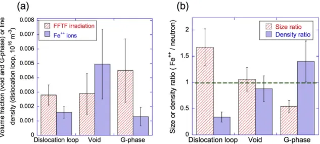
shows the effects of radiation-induced segregation near a grain boundary. Silicon and nickel are enriched, while chromium is depleted. [64] . . . 59 2.21 HT9 samples irradiated to the same dpa with neutrons (in FFTF) and with Fe2+ions exhibit
differences in defect population and typical size or density ratio of those defect populations, indicating that ion irradiation is not necessarily a perfect analog to neutron irradiation. [68] . 61 3.1 TEM images of fluorapatite irradiated with 1 MeV krypton ions show the progression of
amorphization as fluence increases. The TEM allows for imaging and analysis at the atomic level. [77] . . . 66 3.2 Two pulses of laser (the “pump” beams light overlap on a sample (here, illustrated as a thin
film on a substrate). The pulses generate an interference pattern on the sample, resulting in thermal expansion that is proportional to the intensity of the interference pattern. The non-uniform thermal expansion results in the propagation of acoustic waves throughout the sample. These acoustic waves interfere with each other, creating a standing acoustic wave (SAW) on the surface. The SAW can be probed with a second laser beam. This “probe” beam diffracts from the SAW. The signal collected from the diffracted probe beam can be used to analyze the properties of the SAW, and thus the properties of the sample. [114] . . . 70
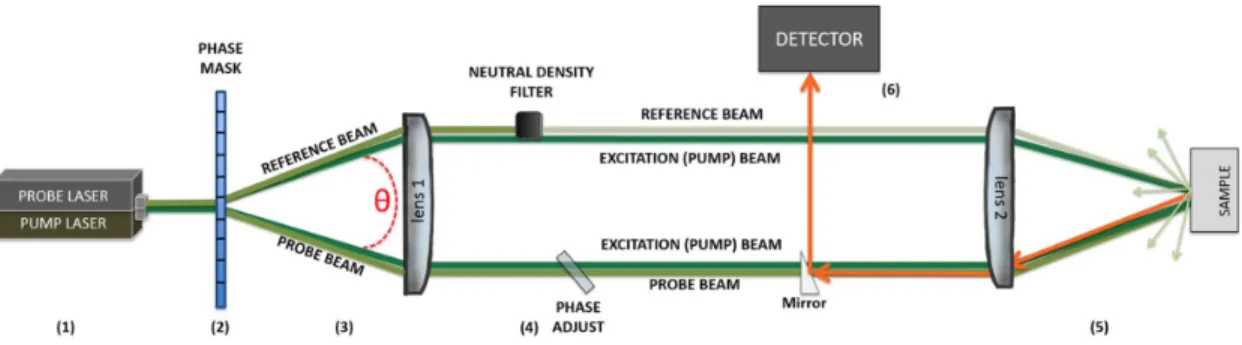
3.3 This schematic was use to explain the TGS setup in the early phases of the project. At (1) the probe and pump laser emit beams that enter the phase mask (2), which determines θ. All diffraction orders of the pump and probe beams are blocked except for the ±1. One order of the probe beam is used as the reference beam, while the other is referred to as the probe beam (3). (This is part of the heterodyne scheme, which is explained in greater detail in the text.) The beams enter lens 1, which sets them back on parallel paths. The reference beam passes through an adjustable neutral density filter to avoid detector saturation, while the probe beam passes through an adjustable glass slide that changes its path length (4). Lens 2 is used to recombine the beams (5), with the sample at the focal point. The SAW is created on the sample surface by the pulsed pump beam and the probe beam and reference beam diffract from the SAW. The diffracted light (the first orders of the probe and reference beams) carries the signal information (orange line), and optics are used to send it to the photodetector (6). . 71 3.4 A long exposure photograph of a TGS experiment in progress in the MIT MNM laser lab.
The green pump beams and red probe beam follow the same path through the setup optics to the sample. The probe beam diffracts from the pump-induced SAW and into the detector. . 72 3.5 The probe beam spot overlaps the pump spot, which creates the transient grating on the
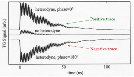
sample surface. The probe spot is smaller than the pump spot to ensure that the probe is not partially capturing the sample surface outside of the excitation region. [119] . . . 72 3.6 The positive and negative traces are amplified by heterodyning. [114] . . . 74 3.7 The positive and negative heterodyne-amplified traces are collected simultaneously with the
new setup, which cuts overall data collection time in half. [123] . . . 75 3.8 A characteristic positive TGS signal. . . 76 3.9 Elastic, acoustic, and thermal properties can be extracted from the TGS signal. . . 77 4.1 Niobium, originally called Columbium, was discovered at the turn of the 19th century by
Charles Hatchett, and is described here in an 1802 journal article. [126] . . . 80 4.2 Modified image from [127] showing experimentally measured changes in Young’s modulus
for three electron-irradiated copper samples with varying levels of cold work. . . 81 4.3 Data from Figure 4.2 replotted (open circles and xs) so it can be compared with the
theoret-ical prediction of (∆E/E)−1/2as a function of integrated flux (straight line). (See p.1417 of
[127].) . . . 81 4.4 A gradual decrease in modulus is observed with extended irradiation. This behavior is not
immediately obvious if only studying material response at low dose. [127] . . . 82 4.5 A typical niobium sample, prior to cold working. Samples are sectioned to be ≈ 1mm thick from a
5mm diameter cylindrical single crystal. This sample is marked with permanent marker for orientation purposes (this can be easily removed with acetone or another solvent). . . 83 4.6 The Carver™ pellet press used to cold work the niobium samples. The lever is used to move
the stage and apply force to the die. . . 84 4.7 A Carver™ 13mm ID pellet die was used for niobium cold working. The stage applies force
to the die’s pushing rod and core die . . . 84 4.8 A schematic showing the interior of the die. The Nb samples were centered in the inner
4.9 A circular niobium sample, photographed through the lens of an optical microscope, is mounted on a metallic block. The area polished with argon ions is visible in the upper half of the niobium - it is a dish-shaped area where the argon ions have begun to erode through the sample. It was very difficult to get a mirror polish surface without also inducing curvature, so the idea of adapting the cross-section polisher for small surface area polishing was abandoned. . . 85 4.10 Selected metallographs of the single crystal niobium polish after MasterPrep polishing, with
bright field images denoted by BF and dark field images denoted by DF. The lefthand images of the control sample show a mostly smooth surface that nevertheless has uniform, if shallow, roughness (especially visible in the dark field view). The sample on the right has been cold-worked, and striations from the sectioning procedure are still visible. The dark field image shows a more noticeable degree of surface roughness (as well as some residue from the Masterprep®. The bottom edge of the metallograph covers an ≈3 mm distance across each sample. These images show that even with extensive polishing using the colloidal silica and the lapping fixture, the samples are not perfectly smooth, and it will be hard to obtain a clear TGS signal on many TGS setups, hence the diamond paper recommendation. . . 86 4.11 Constructive interference occurs when the Bragg condition is satisfied. By maximizing the
intensity of a diffraction spot or pattern created with monochromatic X-rays, various infor-mation about a sample’s crystal structure can be determined. . . 88 4.12 The arrangement of the X-ray source, the sample, and the X-ray detector in a typical XRD
system used in this research. When the diffraction spot intensity is maximized, θ satisfies the Bragg condition, and characteristics of the crystal structure can be determined. . . 88 4.13 A schematic of a typical goniometer. The sample can be moved up (y), side-to-side (x),
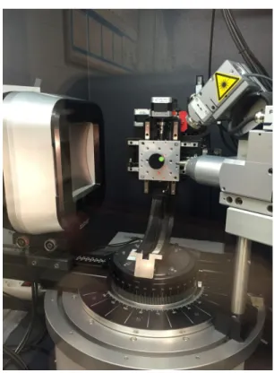
back-and-forth (z), rotated about z (φ), rocked alongΨ, and rotated relative to the detector (ω). Image courtesy of MIT CMSE. . . 89 4.14 The Bruker® system at MIT. The X-ray detector is on the left. The collimated X-ray beam
is on the right. In the middle, the sample is mounted to a cradle that can be moved in six degrees of freedom. The detector and the cradle can be moved relative to each other and relative to the X-ray beam. . . 89 4.15 A frame from a coupled scan of the control sample. The diffraction spot is nearly centered
(χ ≈ −90◦) but is somewhat stretched out, indicating some distortion or imperfection in the
lattice. . . 90 4.16 A frame from a psi scan of the control sample, taken later in the orientation procedure. The
diffraction spot has become more defined as alignment improves, but it still shows a small amount of distortion. . . 90 4.17 An integration of the intensity across diffraction spot in Figure 4.16. . . 91 4.18 A frame from a coupled scan of the 1000 lb sample. The diffraction spot is off-center (χ ≈
−90◦) and stretched, indicating some distortion or imperfection in the lattice and a significant amount of miscut. . . 91 4.19 A frame from a psi scan of the 1000 lb sample. The diffraction spot is more centered in this
frame, but is faint and distorted. . . 91 4.20 A frame from one of the φ scans performed on the 1000 lb sample. The diffraction spot did
not come into the center of the frame during these scans. . . 92 4.21 A frame from a coupled scan of the 1500 lb sample. The diffraction spot appears close to
the center of the frame (χ ≈ −90◦) and is stretched more obviously than the previous two
4.22 Integrating a frame from the coupled scan shows two distinct regions of intensity on either
side of χ=90◦. . . . 93
4.23 A frame from a coupled scan of the 2000 lb sample. The diffraction spot appears close to the center of the frame (χ ≈ −90◦) and exhibits a level of distortion similar to that of the 1500 lb sample. . . 94
4.24 Integrating a frame from the coupled scan shows an asymmetric intensity peak: it is possible that this asymmetry is due to non-isotropic distortion of the sample. χ is about 4◦off from -90◦. . . 94
4.25 A frame from a coupled scan of the 2400 lb sample. The diffraction spot appears close to the center of the frame (χ ≈ −90◦) but note that the 2θ value is not optimized for the<011> orientation. . . 94
4.26 Integrating a frame from the coupled scan confirms that the sample is well-aligned to the reference orientation. . . 94
4.27 A frame from a coupled scan of the 3000 lb sample. The diffraction “spot” stretches along the arc defined by a single 2θ value, with varying intensity. Integration of intensity as a function of χ shows two main intensity peaks. One is about 30◦off from χ = −90◦, while the other is about 20◦off. . . 95
4.28 Control φ scan . . . 96 4.29 1000 lb φ scan . . . 96 4.30 1500 lb φ scan . . . 96 4.31 2000 lb φ scan . . . 96 4.32 2500 lb φ scan . . . 96 4.33 3000 lb φ scan . . . 96
4.34 Pole figures for the control sample . . . 99
4.35 Pole figures for the 1500 lb sample . . . 99
4.36 Pole figures for the 2000 lb sample . . . 99
4.37 Pole figures for the 1000 lb sample . . . 100
4.38 Pole figures for the 2500 lb sample . . . 100
4.39 Pole figures for the 3000 lb sample . . . 100
4.40 HRXRD rocking curves for the control sample, 1500 lb sample, and 2000 lb sample. There is a significant difference between the control sample and the other two samples. Based on these curves, 1500 lb and 2000 lb likely have a very similar dislocation density. . . 101
4.41 The 1000 lb, 2000 lb, and 3000 lb samples are plotted separately, as they have a different orientation than the other samples. Note that the 1000 lb sample - the most intense peak here - is only about 20% the height of the control sample rocking curve. . . 102
4.42 Dislocation density in the cold-worked niobium samples, as estimated from Equations (4.5) and (4.4). A steady buildup of dislocations is observed until 1500 lbs of cold work, at which point a saturation seems to be reached. At 2500 lbs of cold work, dislocation density increases again. . . 103
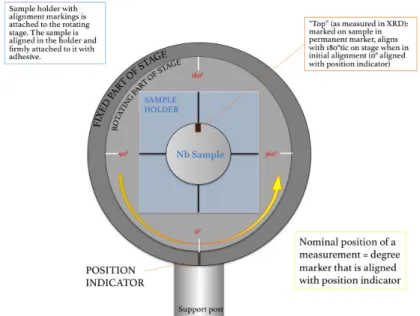
4.43 The schematic shows the niobium sample mounted on the rotating stage used to make the measurements. For clarity, the sample depicted here is much larger relative to the stage than it is in practice. . . 105
4.44 All individual TGS measurements taken on the cold-worked Nb samples. Each measurement consisted of three traces, which are averaged here. This data is plotted prior to shifting data sets so that maxima align. . . 106
4.45 TGS data from the cold-worked niobium samples. This is the same data plotted in Figure 4.44, but the measurements at each position have been averaged and the data sets have been shifted relative to each other to align maxima. Error bars have also been added. . . 107 4.46 Calibrated grating spacing for each day of niobium measurements, showing that the grating
spacing varied by as much as 0.04µm from day to day. The collection of calibration data for every day of measurement is therefore an important step to ensure that analysis of the TGS data reflects the physical properties of the samples as accurately as possible. The nominal grating spacing for all measurements was 5.5µm. . . 108 4.47 vS AW results for the first group of cold-worked niobium samples, graphed alone for easier
comparison. It is possible that the 2000 lb sample has undergone a small decrease in Young’s modulus in the fast direction, but overall, the behavior of the samples with respect to SAW speed as a function of surface rotation is remarkably consistent despite the differences in cold work between them. . . 108 4.48 vS AW results for the second group of cold-worked niobium samples. These samples show a
more significant variation in behavior than do the group 1 samples. . . 109 4.49 The data for the cold-worked samples, separated by group and plotted as the ratio of∆vS AW
to vmin, where∆vS AW = v(θ) − vmin, and vminis the minimum vS AW observed for the control
sample. . . 110 4.50 Rotational translations used in the numerical TGS predictions. For the purposes of this
project, first two translations correspond to the offset of a sample’s true alignment from an arbitrary alignment. . . 111 4.51 The black line shows experimental data for SAW speed versus degree of surface rotation for
the control sample. The blue and red lines are the predicted SAW response for 0◦and 15◦of tilt. These results are given for rotations of 0 to 90◦in 10◦increments. . . 112 4.52 The black line shows experimental data of the SAW speed versus degree of surface rotation
for the control sample. The colored lines are the predicted SAW speeds as a function of surface rotation for an<011> oriented single crystal, with a 0d rotational offset and varying amounts of tilt offset. The arrow shows the direction of increasing tilt. . . 114 4.53 The slowness surface for {110} single crystal Nb shows that PSAW and SAW behavior will
be observed. . . 114 4.54 At certain surface rotations, the SAW response for the 0◦rotation condition for<011> single
crystal Nb is small compared to the PSAW response. However, the algorithm “picks” the response by selecting the first response from the right, and so it only “sees" the small SAW response. This explains the dips observed in the calculated responses graphed in Figure 4.52. The experimental setup still captures the PSAW response, which is why the experimental data looks like a smooth sinusoid-esque curve. . . 114 4.55 The black line shows experimental data of the SAW speed versus degree of surface rotation
for the 1000 lb sample. The blue and red lines are the predicted SAW response for 0◦ and 15◦ of tilt. These are given for rotations of 0 to 95◦in 5◦increments. Other tilt conditions have been omitted. . . 115 4.56 vS AW was measured as a function of surface rotation of the control sample following
irradi-ation with Si3+ions to 0.01, 0.03, 0.1, and 1 dpa. Data sets have been shifted horizontally to align maxima. . . 119 4.57 vS AW was measured as a function of surface rotation of the control sample following
irradi-ation with Si3+ions to 0.01, 0.03, 0.1, and 1 dpa. Data sets have been shifted horizontally to
4.58 vS AW was measured as a function of surface rotation of the control sample following
irradi-ation with Si3+ions to 0.01, 0.03, 0.1, and 1 dpa. Data sets have been shifted horizontally to
align maxima. . . 121 4.59 vS AWwas measured as a function of surface rotation of the control sample following
irradia-tion with Si3+ions to 0.01, 0.03, 0.1, and 1 dpa over 180-200◦. This graph shows the results
of averaging all speed measurements taken on a given sample after each irradiation. Error bars are large in part due to the normal spread of vS AW on the anisotropic single crystal. . . . 122
4.60 vS AW in the fast direction (although some of the data points in the average are likely PSAW
responses, as explained on page 113. All vS AW measurements ±5◦from the rotational
posi-tion of the measured maximum vS AWare averaged. . . 122
4.61 Thermal diffusivity results, control sample. Error bars are not shown for clarity. The associ-ated error for each thermal diffusivity measurement was on the order of 10−7m2/s. . . 123 4.62 Acoustic damping results, control sample . . . 124 4.63 Thermal diffusivity results for all samples after cold working (0 dpa) followed by irradiation
to 0.01, 0.03, 0.1, 1, and 3 dpa. Points represent the average of all measurements. Error was an order of magnitude lower than the average and is not plotted for clarity, since the primary data points overlap in places. . . 125 4.64 The data in Figure 4.63 is replotted with dose on a log scale. The thermal diffusivity is
observed to drop at low doses, rise again, and saturate near 2E-5 m2/s. The 0 dpa data are
assigned a pseudo-dose of 0.001 dpa here to keep them on the graph. However, the response between 0 dpa and 0.01 dpa is unknown, so it may not be accurate to consider the 0.001 dpa response as a reasonable approximation for the known 0 dpa response. . . 125 4.65 Acoustic damping results for all samples after cold working (0 dpa) followed by irradiation
to 0.01, 0.03, 0.1, 1, and 3 dpa. Points represent the average of all measurements. The procedure for calculating acoustic damping is still being refined, and these measurements should be considered as estimates only. Error is on the order of 10−9, including for the (1 dpa, 1500 lb) point. . . 126 4.66 The data in Figure 4.65 is replotted with dose on a log scale. As before, the 0 dpa data are
assigned a pseudo-dose of 0.001 dpa. The data plotted between 0.01 and 0.1 dpa indicate evidence of an exponential relationship between acoustic damping and dose. . . 126 4.67 SAW speed in the fast direction at 0 dpa for the control, 1500 lb, and 2000 lb single crystal
niobium samples. . . 129 4.68 Oxygen impurities in single crystal niobium are mobile during neutron irradiation, and are
trapped at radiation-induced defect clusters (dark spot). [147] . . . 131 4.69 Dislocation density of niobium samples irradiated with 5 MeV protons rises sharply at low
dose (0.01 dpa) as radiation damage builds up in the bulk. As dose increases, these defects concentrate into larger defects that are less dispersed through the bulk. These results were confirmed via TEM. Adapted from [148] . . . 131 5.1 Thermal vacancy concentration in aluminum and niobium as a function of temperature. . . . 135 5.2 The NiAl phase diagram . . . 136 5.3 The phase diagram above, annotated . . . 137 5.4 The structure of B2-phase NiAl consists of a simple cubic lattice of Ni atoms interlocked
5.5 The lattice parameter of B2-phase NiAl varies with composition. The lattice parameter reaches a maximum near the stoichiometric point. It decreases as the nickel content goes down relative to the stoichiometric point and the number of nickel vacancies goes up. It decreases at a more gradual slope as the nickel content increases relative to the stoichio-metric point and the number of nickel anti-site defects on the aluminum sublattice goes up. Citations for the data plotted are as follows: “Cooper1963”, [164]; “Jacobi1971”, [165]; “Hughes1971,” [166], and “Kogachi1996”, [167]. . . 139 5.6 Reported concentrations of structural vacancies present in NiAl as a function of composition
from select literature. Note that the “Pike1997” and “Kogachi1996” report CNi
V values of ≈ 0
for at% Ni ≥ 50%, while the 2001 update to Kogachi1996 reports a CNiV at 52 at% Ni that is ≈ CVNi(50% Ni)≈ 9%. The updated Kogachi data is also significantly higher than the other data sets, with reported CVNiof over 12% at lower values of nickel concentration. Interestingly, Kogachi also reports nonzero CAlV, although it never exceeds 2%. For less than 50% Ni, CVNi decreases monotonically with increasing Ni concentration. Citations for the data plotted are as follows: “Kogachi1996”, [167]; “Kogachi1996 updated”, [172]; and “Pike1997,” [173]. . 140 5.7 The plot of magnetic susceptibility as a function of composition illustrates that NiAl has
very different material properties on either side of the stoichiometric composition. Adapted from [174]. . . 141 5.8 The plot of magnetic resistivity as a function of composition illustrates that NiAl has very
different material properties on either side of the stoichiometric composition. Resistivity increases with increasing defect concentration: above the stoichiometric point, resistivity increases as the concentration of nickel vacancies increases, and below the stoichiometric point, resistivity increases as the concentration of nickel anti-site defects increases. [174] . . 141 5.9 Dislocations in an NiAl sample used in [159] . . . 144 5.10 The NiAl phase diagram . . . 145 5.11 Ni/Al powder mixture is transferred to the pellet press die using a funnel and a disposable
scoop . . . 146 5.12 A vacuum pump (connected to the tube) is used to remove air while samples are pressed. . . 146 5.13 The finished pellets are about 0.5” wide and 0.25” high. The pellets are much easier to
handle than the loose powders, especially during the arc melting step. . . 146 5.14 The MIT MNM arc melter in use. The user controls the position of the arc and the power
supplied to the electrode. Welders’ glass windows allow the user to see when the pellets have fully melted and formed a single button of molten material. . . 147 5.15 The five buttons made in the arc melter were heat treated in a high-temperature graphite
furnace under an inert environment for 24h at 1200◦C. The photograph shows the buttons
arranged in the furnace prior to beginning the heat treatment. The purpose of the heat treat-ment was to grow large grains, so that the TGS measuretreat-ments could be easily carried out within the boundaries of a single grain if the buttons were used for measurements. The furnace pictured here is in the Allinore lab at MIT. . . 147 5.16 NiAl sample #1 at 50x magnification in a polarized field. The etchant swab created shallow
“scratches” that make it difficult to see the sample’s features. . . 148 5.17 NiAl sample #2 at 50x magnification in a polarized field. As with #1, the etching
pro-cess obscured many of the features on this sample. This is exacerbated by the small voids throughout sample that seem to have formed during melting. . . 148
5.18 NiAl sample #3 at 50x magnification in a bright field. It is easier to see the large grains, some of which are several hundred µm in width and thus capable of fitting the entire TGS
spot. . . 148
5.19 A second image of NiAl sample #3 at 50x magnification in a bright field, showing the large, clearly delineated grains. . . 148
5.20 NiAl sample #4 at 50x magnification in a bright field. As was the case with Sample #2, small voids developed during the arc melting process. . . 148
5.21 NiAl sample #5 at 50x magnification in a bright field. Voids appear to be distributed through this sample as well, although they appear smaller than the voids observed in #1 and #4. . . . 148
5.22 Degrees of freedom in the sample mount for the Bruker® D8 GADDS system, taken from the MIT CMSE SOP for the equipment. . . 150
5.23 A photograph of an NiAl sample in the XRD GADDS system. The wide-angle germanium detector is on the left and the X-ray source is on the right. The sample’s cradle moves in x, y, z, φ, ψ, and ω. The entire cradle and the detector move independently to change the angle between the detector and the X-ray source (2θ) and the angle between the detector and the sample. . . 150
5.24 The schematic shows the mounted sample and the corrections required to make the <100> direction normal to the measurement surface. ω involves rotating the sample from side to side, whereas ψ indicates a back-and-forth tilt. . . 151
5.25 A not-to-scale schematic of the process of cutting the sample mount to correct for misalign-ment of the crystal plane relative to the TGS measuremisalign-ment surface. Sample planes (shown as light blue lines) have a misalignment of ψ. By making a cut at an angle of ψ from the back of the mount, we bring the crystal planes into their proper alignment when the back of the mount is level. A second cut is then made because the measurement surface needs to be flat. The new surface is repolished prior to measurement. . . 152
5.26 1A, bright field (41.18 Ni, 58.73 Al, 0.04 Fe, 0.05 Si) . . . 157
5.27 1A, dark field (different region). The large voids are the most distinctive features here. . . . 157
5.28 1A, polarized (same region as dark field) . . . 157
5.29 1B (41.98 Ni, 57.95 Al, 0.03 Fe, 0.04 Si ) polarized. Grains are large and very distinct under polarized light for the samples with < 42 at% Ni. . . 157
5.30 #2, bright field (44.11 Ni, 55.76 Al, 0.08 Fe, 0.04 Si). Large population of mid-dized (10-20µm) voids. . . 157
5.31 #2, dark field (different region) . . . 157
5.32 #2, polarized (same as dark field). Grain boundaries are more evident, but look distinctly different from those observed in Nos. 1A and 1B. . . 157
5.33 #3, bright field (44.51 Ni, 55.37 Al, 0.06 Fe, 0.05 Si . . . 158
5.34 #3, dark field (different region) . . . 158
5.35 3, polarized (same region as dark field) . . . 158
5.36 #6, bright field (44.58 Ni, 54.32 Al, 0.08 Fe, 0.03 Si) . . . 158
5.37 #6, dark field (different region) . . . 158
5.38 #6, polarized (different region) . . . 158
5.39 #4, bright field (47.38 Ni, 52.53 Al, 0.05 Fe, 0.04 Si (at%)) . . . 158
5.40 #4, dark field (different region) . . . 158
5.41 #4, polarized (different region) . . . 158
5.42 #5, bright field (47.73 Ni, 52.16 Al, 0.07 Fe, 0.04 Si (at%)) . . . 159
5.44 #5, polarized (different region) . . . 159
5.45 #7, bright field (49.01 Ni, 50.90 Al, 0.06 Fe, 0.04 Si) . . . 159
5.46 #7, dark field (different region) . . . 159
5.47 #7, polarized (different region) . . . 159
5.48 #8, bright field (49.97 Ni, 49.94 Al, 0.06 Fe, 0.04 Si) . . . 159
5.49 #8, dark field (different region) . . . 159
5.50 #8, polarized (different region) . . . 159
5.51 #9, bright field (57.47 Ni, 42.43 Al, 0.07 Fe, 0.02 Si) . . . 160
5.52 #9, dark field (different region) . . . 160
5.53 #9, polarized (different region) . . . 160
5.54 #10, bright field (59.63 Ni, 40.31 Al, 0.04 Fe, 0.02 Si (at%)) . . . 160
5.55 #10, polarized (different region) . . . 160
5.56 SAW speed measurements on NiAl of varying compositions taken at a nominal 5.5µm grat-ing spacgrat-ing. These samples were not corrected for possible miscut or misalignment of the crystal planes. Data was shifted in degree so that the first maximum in each data set was matched. . . 164
5.57 An attempt to match the unknown, crystallographically corrected “blue” sample to a sample of known composition was made. The best match was Luvak 4. If Luvak4 and “Blue” were from the same sample, then this indicates that the angling step was probably unnecessary. . . 165
5.58 An attempt to match the unknown, crystallographically corrected “pink” sample to a sample of known composition was made. The best match was Luvak5. As with Figure 5.27, if we can assume that the unknown sample comes from the same single crystal rod as the identified sample whose response it most closely matches, then it would appear that the angling steps had little effect on the frequency (and therefore the speed) response. . . 165
5.59 SAW speed vs. at% NiAl for Batch I and Batch II samples. Results show a general de-crease in speed on the Al-rich side of the compositional range as the stoichiometric point is approached (direction of decreasing vacancy concentration). . . 166
5.60 Linear fit to the vS AW data for 44 to 50 at% Ni . . . 167
5.61 Young’s modulus of NiAl versus vacancy concentration in NiAl, calculated from Equation (5.10). . . 169
5.62 Microhardness increases with vacancy concentration in intermetallic FeAl. [181] . . . 170
5.63 Microhardness increases with vacancy concentration in intermetallic FeAl. [181] . . . 170
5.64 Thermal diffusivity as a function of at% nickel in NiAl polycrystalline and single crystal samples. . . 171
5.65 Linear fit to the thermal diffusivity data for samples with composition 44-50 at% Ni. . . 173
5.66 Acoustic damping as a function of at% nickel in NiAl polycrystalline and single crystal samples. . . 174
5.67 The TGS simulation begins with a structure with a free surface. . . 176
5.68 Two regions on the free surface are specified for center-of-mass tracking. . . 176
5.69 A sinusoidal heat pulse is applied to the free surface. . . 176
5.70 Initial relaxation of nickel and aluminum test structures in LAMMPS was unsuccessful. The test structures were random mixes of Ni and Al, but did not replicate the actual structures of B2-phase NiAl. Instead, lattice parameter simply grew with the increasing nickel content, as nickel is the larger atom. . . 177 5.71 Results of convergence tests showed that the test structure should have at least 2 million atoms.179
5.72 A stoichiometric NiAl structure constructed in MATLAB, and a Ni-poor NiAl structure with a significant concentration of constitutional vacancies constructed using the same code, are pictured. MATLAB is used to create input text files that rebuild these structures in LAMMPS. 179 5.73 Lattice parameter results for B2-NiAl obtained in LAMMPS compared against lattice
pa-rameters reported in the literature. . . 181 5.74 SAW speed measured from TGS simulations carried out on NiAl test structures of 2×10⁶
lattice spots in LAMMPS. . . 182 5.75 SAW speed measured from TGS simulations carried out on NiAl test structures of 2×10⁶
lattice spots in LAMMPS. . . 183 5.76 Measurements on the Batch I samples taken over the full surface rotation (with at least two
spots per rotation position) during a previous data collection campaign are included with the data sets to provide a better picture of the single crystal behavior. Error values for these points were on the order of 1% of the averaged measurement value. . . 185 6.1 A radioactive hex block in a hot cell after removal from the EBR-II reflector. The block is
5.2 cm wide and about 20cm long. [189] . . . 189 6.2 Radiation damage response is not uniform throughout each block due to neutron flux and
temperature gradients that existed throughout the block. The temperature peaked near the middle, but the peak was shifted toward the side that was nearest to the reactor core. Gamma heating and dpa rate increased monotonically from the side furthest from the reactor core to the side closest. Schematic from [189] . . . 189 6.3 The image, modified from [190], shows where the tested samples came from in the EBR
core. The blocks (5 and 3) are marked with stars; the sections of those blocks relevant to this study are marked with yellow arrows. The blocks were stacked in a hexagonal duct with 1 mm thick 304 stainless steel walls. The duct was located in Row 8 of the core’s reflector region [189]. . . 190 6.4 The image, from [190], shows where Sample 3D1 was located in Coin 3D, as well as its
dimensions.D signifies that the sample was immersion density measured. . . 191 6.5 Sample 3D1 was divided into five sections. The larger sections in the middle three (3DB1,
3D1C, and 3D1D) were each further divided into four subsections. One subsection from each of 3D1B, 3D1C, and 3D1D were used in this study. . . 191 6.6 The image, from [190], shows where Sample 3E1 was located in Coin 3E, as well as its
dimensions.D signifies that the sample was immersion density measured. . . 191 6.7 Sample 3E1 was divided into five sections. Section 3E1B was divided into three sections.
The middle section, 3E1B1, was divided into four more sections, two of which were thin slices intended for use in making TEM samples. One of these thin slices, 3E1B1A, is used here. [190] . . . 191 6.8 The image, from [190], shows where Sample 5A1 was located in hex coin 5A. Sample 5A1
was divided into five sections, one of which, 5A1B, is relevant to this work. . . 192 6.9 Section 5A1B was divided into three more sections. The middle piece, 5A1B1, was divided
into four more sections, two of which were thin slices intended for use in making TEM samples. One of these thin slices, 5A1B1B, is used in this work. Both this figure and Figure 6.8 are from [190]. . . 192
6.10 5B1 of hex coin 5B was divided into four sections. The two middle sections, 5B1B and 5B1C, were each divided into four more sections. As in previous coins relevant to this work, two of these sections were thin slices. One thin slice from each of 5B1B and 5B1C were used in this work: 5B1B2B and 5B1C2B. [190]. . . 192 6.11 5C1 of hex coin 5C was divided into three sections. The middle section, 5C1B, was divided
into four more sections. As in previous coins relevant to this work, two of these sections were thin slices. One of the thin slices, 5C1B2B, was used in this work. [190]. . . 192 6.12 Micrographs of the archival stainless steel hex block, which serves as the stock for the control
sample used in the TGS project. The archival block indicates that the blocks were cold worked prior to placement in EBR-II. [189] . . . 195 6.13 Flat-to-flat swelling for Blocks 2, 3, and 4; a schematic for visualizing the direction of the
flat-to-flat measurements; and lengthwise swelling in Blocks 3 and 5. Block 3, in the center of the stack, exhibited the most dramatic swelling. Block 5 was at the top of the stack. Lengthwise measurements show that Block 3 exhibited significant expansion, whereas Block 5 did not. INL and WEC indicate the hot cell in which the measurements were made - Idaho National Laboratory or Westinghouse Electric Company. Negative swelling values in Block 2 and Block 4 indicate carbon densification has taken place. Flat-to-flat swelling data for Block 5 is presented in Figure 6.14. [189] . . . 196 6.14 Post-irradiation flat-to-flat dimensions for Block 3 and Block 5. The solid line at 2.062”
shows the nominal dimension of the block prior to irradiation. Block 3, which received the higher dose, clearly exhibits swelling behavior that clearly exceeds the nominal+tolerance flat-to-flat length. The amount of swelling from flat-to-flat varies with axial position. Block 5 exhibits negative swelling, which is associated with carbon densification. Note that left-to-right indicates bottom-to-top. [189] . . . 197 6.15 Acoustic velocity mapping (lengthwise) for Block 3. Acoustic mapping for coin 3E from
this angle and of Block 5 was not provided. Section 3D (the side of hex coin 3D) exhibits a variation of acoustic speed of about 20 m/s. The archival (unirradiated) acoustic velocity is 5735 m/s. [189] . . . 198 6.16 An acoustic map of hex coin 3D shows that the lowest speeds are clustered slightly
off-center - the same spot where the highest concentration of voids is expected to be and where radiation damage was highest. The coins from block 3 exhibit a large acoustic velocity gradient, with variations of up to 70 m/s. [189] . . . 199 6.17 An acoustic maps of hex coins shows velocity increases relative to the nominal acoustic
speed of the archival material (5735 m/s). The changes are less severe than those observed in block 3, with acoustic speed variations of about 30 m/s. [189] . . . 199 6.18 An acoustic map of hex coin 3E, overlaid with density results. Note that the image is flipped
relative to the image in Figure 6.16, with the flats on opposite sides. The low-velocity region occurs in the same place on each coin. Coin 3E was sectioned according to the dashed lines, and density measurements were made on each segment. The extent of the density change corresponded with the extent of the acoustic velocity reduction. [189] . . . 200 6.19 TEM images of a sample from coin 3E show many voids dispersed throughout the
mate-rial.Hex block 3 was in the center of the stack and received the highest radiation dose. [191] 200 6.20 Hex block 5 received a much lower dose than hex block 3. A few voids are visible in this
coin 5D sample, but the difference in void density visible in this image and in the images of coin 3E is obvious. [191] . . . 201
6.21 The table from [193] that quantitatively characterized voids, precipitates, and Frank-Reed loops, based on TEM of the EBR-II samples. Stars are added here to show which rows cor-respond to a sample that was immediately adjacent to the samples used in this study prior to the samples being cut from the hex blocks. It is assumed that the defect populations of the samples in this study are effectively equivalent to the defect populations of their correspond-ing samples in [193]. . . 202 6.22 SAW speed measurements, averaged by sample and plotted by the dpa to which each sample
was irradiated in EBR-II. . . 204 6.23 SAW speed measurements, with all data grouped by hex block. Hex block 5 (second point)
is plotted at 2.625 dpa, which is the average of the dpa values reported for each sample measured here that originated in hex block 5. Hex block 3 (rightmost point) is plotted at 28 dpa, which was the reported dpa value for every sample measured here that originated in hex block 3. . . 205 6.24 Thermal diffusivity measurements, averaged by sample and plotted by the dpa to which each
sample was irradiated in EBR-II. . . 205 6.25 Void density as measured in [193] versus TGS-measured SAW speed . . . 206 6.26 Void density as measured in [193] versus TGS-measured thermal diffusivity . . . 206 6.27 Void swelling as measured in [193] versus TGS-measured SAW speed . . . 206 6.28 Void swelling as measured in [193] versus TGS-measured thermal diffusivity . . . 206 6.29 Precipitate density as measured in [193] versus TGS-measured SAW speed . . . 207 6.30 Precipitate density as measured in [193] versus TGS-measured thermal diffusivity . . . 207 6.31 Frank loop density as measured in [193] versus TGS-measured SAW speed . . . 207 6.32 Frank loop density as measured in [193] versus TGS-measured thermal diffusivity . . . 207 6.33 Frank loop length density as measured in [193] versus TGS-measured SAW speed . . . 207 6.34 Frank loop length density as measured in [193] versus TGS-measured thermal diffusivity . . 207 6.35 Neutron irradiated stainless steels undergo an increase in yield strength σy at doses that
correspond to the doses incurred by the EBR-II samples, which corresponds to an increase in E. The irradiation temperatures to which the EBR-II samples were exposed was in the 400-420◦C range, well below the range at which temperature would be expected to be associated with a decrease in σy. [197] . . . 209
6.36 304 stainless steel stress-strain test results, prior to irradiation. [196] . . . 209 6.37 304 stainless steel stress-strain test results, following irradiation to 30 dpa in the High Flux
Reactor in Petten, the Netherlands. [196] . . . 209 6.38 APT results for 304 steel irradiated to 5 dpa with protons shows evidence of
radiation-induced segregation. A grain boundary in the APT sample is indicated for the Si scan with a black arrow. These results show slight depletion at the grain boundary for Fe, Cr, Mn, and Cu, and enrichment at the grain boundary for Si, P, B, and S. Enrichment is particularly dramatic for the Si, P, and B species. [203] . . . 210 6.39 APT data of 304 stainless steel samples irradiated to 0.4 dpa (a) and 28 dpa (b) in EBR-II
shows evidence of precipitation of Ni and Si from the Fe matrix. [209] . . . 211 6.40 APT data of a 304 stainless sample irradiated to 0.4 dpa in EBR-II shows evidence of
pre-cipitation of P from the Fe matrix. [209] . . . 212 6.41 APT data of 304 stainless steel samples irradiated to 28 dpa in EBR-II shows evidence of
precipitation of P from the Fe matrix. [209] . . . 212 6.42 Thermal diffusivity measured by TGS versus void density measured via TEM analysis in [193]213 6.43 Average void diameter versus void density, both measured via TEM analysis in [193] . . . . 213
6.44 Dpa associated with samples versus their void density measured via TEM analysis in [193] . 213 7.1 TGS enables more efficient radiation materials science research campaigns. Schematic by
M. P. Short. . . 217 8.1 Orientation distribution function obtained from the pole figure data of the control Nb sample 220 8.2 Orientation distribution function obtained from the pole figure data of the 1000 lb Nb sample 221 8.3 Orientation distribution function obtained from the pole figure data of the 1500 lb Nb sample 222 8.4 Orientation distribution function obtained from the pole figure data of the 2000 lb Nb sample 223 8.5 Orientation distribution function obtained from the pole figure data of the 2500 lb Nb sample 224 8.6 Orientation distribution function obtained from the pole figure data of the 3000 lb Nb sample 225 8.7 The black line shows experimental data for SAW speed versus degree of surface rotation for
the 1500 lb sample, which is expected to be well-aligned to the<110> plane. The blue and red lines are the predicted SAW response for 0◦and 15◦of tilt. These are given for rotations of 0 to 95◦in 5◦increments. Other tilt conditions have been omitted. . . 232
8.8 Experimental data and predicted SAW speed calculations as a function of surface angle for the 2000 lb sample . . . 233 8.9 Experimental data and predicted SAW speed calculations as a function of surface angle for
the 2500 lb sample . . . 233 8.10 Experimental data and predicted SAW speed calculations as a function of surface angle for
the 3000 lb sample . . . 234 8.11 Thermal diffusivity results, 1500 lb sample . . . 235 8.12 Acoustic damping results, 1500 lb sample . . . 236 8.13 Thermal diffusivity results, 2000 lb sample . . . 236 8.14 Acoustic damping results, 2000 lb sample . . . 237 8.15 Elastic constants of NiAl as reported in [161]. . . 239 8.16 Elastic constants of intermetallic NiAl of various concentrations as a function of
tempera-ture, from [161]. . . 240 8.17 NiAl tends to deform by glide in the<100> family of directions in the {011} and {001}
plane families. Above, the [100] direction in the (011) and the (001) planes of a B2-structured system is illustrated. . . 241 8.18 On the left, Young’s modulus is graphed as a function of temperature. The top three lines
(45-50 at% Ni) correspond to NiAl compositions that we consider in our work. The modulus decreases with temperature. These values are close to the values computed from single crystal data. [175] . . . 242 8.19 Example LAMMPS output code generated by the MATLAB script for a relatively small
structure of about 2000 atoms showing the header script and the x-y-z specifications for the first seven atoms. . . 245
List of Tables
3.1 Advantages and disadvantages of various destructive radiation damage characterization meth-ods,$= no,"= yes,≈= possible . . . 67 3.2 TGS setup parameters used in this thesis . . . 75 4.1 Crystallography peak list for pure niobium . . . 90 4.2 Summary of XRD characterization of cold-worked niobium sample orientations . . . 97 4.3 HRXRD rocking curves of the cold-worked single crystal Nb samples . . . 102 4.4 Irradiation parameters for the cold-worked irradiated niobium study: integrated charge in
10−11C to reach each dpa level (given in italics), and actual charge achieved during each irradiation step for each sample . . . 118 5.1 Preparing NiAl specimens: some examples from six decades of literature . . . 143 5.2 Composition plan for sample matrix, NiAl Batch I . . . 145 5.3 Growing single crystal samples at LANL from the arc-melted and annealed NiAl buttons . . 149 5.4 Sample tilts as measured by XRD. Figure 5.24 illustrates ω and ψ relative to the mounted
sample (oriented in φ). Each sample had a color label for easy identification. . . 151 5.5 Composition of NiAl Batch I . . . 153 5.6 Planned compositions for NiAl Batch II . . . 155 5.7 Composition of NiAl Batch II . . . 155 6.1 EBR-II sample history and description, as provided by Westinghouse . . . 194 6.2 Dose and temperature range for select hex coins, as reported in [191] . . . 194 6.3 TGS-measured SAW speed and thermal diffusivity for the EBR-II samples . . . 204 8.1 Elastic constants decrease with increasing vacancy concentration, as reported in [161] . . . . 239
Nomenclature
α Alpha particle
¯
νe Antineutrino
β β particle
β- Indicates B2-phase intermetallic structure β+ Positron that has been emitted in β-decay
β− Electron that has been emitted in β-decay
βΩ Integral breadth of peak in HRXRD
χ Tilt (front to back) of sample [XRD applications]
γ Gamma ray λ Wavelength ˚ A Angstrom (10−10m) µ Micro-; ×10−6 µ Shear modulus ν Frequency νe Neutrino
ω Degree of tilt (left to right) [XRD applications]
Φ Radiation flux [bombardment applications]
φ Degree of surface rotation [XRD applications]
φ Radiation flux [bombardment applications]
σ Standard deviation [error calculation applications]
σ Tensional stress
σD Displacement cross section
σy Yield strength
θ Bragg’s angle [XRD applications]
θ Surface rotation angle [TGS applications]
ε Extensional strain ◦ degree i Indicates interstitial v Indicates vacancy A Atomic weight b Burgers vector Cv Vacancy concentration
Ci jkl Elastic tensor entry
d Average obstacle size [dislocation movement] d Lattice spacing [X-ray diffraction applications]
E Energy
E Young’s modulus
Ed Displacement energy
Ei Initial or impinging energy of radiation
Hv Enthalpy of vacancy formation
N Number density of a material (number of atoms per unit volume) N Total number of measurements [error calculation applications]
Nd Number of displacements per atom
R Gas constant, 8.3144598 kg m2s−2K−1mol−1
R Range of particles in a target [bombardment applications]
S Stopping power
Td Damage energy; energy available for displacements
vS AW Speed of surface acoustic wave, typically reported in [m/s]
x 1D distance into target
Z Atomic number
’ Feet
” Inches
<x y z> indicates a family of crystallographic directions
C Coulomb
C Elastic tensor
A Ampére
APT Atom probe tomography
ASD Anti-site defect
at% Atomic percentage
BF Bright field [optical microscopy]
C Degrees Celsius
c Speed of light (2.99792458 m/s)
CANDU Canada Deuterium Uranium reactor
CMSE Center for Materials Science and Engineering at MIT
DF Dark field [optical microscopy]
dpa Displacements per atom; used as a pseudo-unit to describe radiation damage in material
dpa Displacements per atom
e Elementary charge (1.602 ×10⁻¹⁹C )
EBR Experimental Breeder Reactor
EDX Energy-dispersive X-ray spectroscopy
eV Electronvolt (work to accelerate an electron through a one volt potential difference)
f Frequency
FIB Focused ion beam
FWHM Full width at half maximum
g Grams
GADDS General Area Detector Diffraction System
GFR Gas-cooled fast reactor
GS Grating spacing (typically used as a subscript, e.g. λGS
h Hours
HOLOSLAM Holographic scanning laser acoustic microscopy HRXRD High-resolution X-ray diffraction
HV Hardness value
ICP Inductively-coupled plasma
ID Inner diameter
K Degrees Kelvin
lb Pound
LFR Lead-cooled fast reactor
LSAW Laser-induced surface acoustic wave
M Mega-; ×106
m Meter
MD Molecular dynamics
MIT Massachusetts Institute of Technology MIT MNM MIT Mesoscale Nuclear Materials group
mol Moles [1 mol= 6.022×10²³]
MSR Molten salt reactor
PKA Primary Knock-on Atom
ppm Parts per million
rpm Rotations per minute
RUS Resonant ultrasound spectroscopy
s Seconds
SAM Scanning acoustic microscopy
SAW Surface acoustic wave
SBS Surface Brillouin scattering
SCWR Supercritical water reactor
SEM Scanning electron microscope
SFR Sodium0cooled fast reactor
SLAM Scanning laser acoustic microscopy
SRIM Stopping Range of Ions in Matter computer program
T Temperature
TEM Transmission electron microscopy
TGS Transient grating spectroscopy
V Volt
VHTR Very-high-temperature reactor
W Weight
wt% Weight percent
Chapter 1
Prologue:
Breaking the bottleneck in nuclear
materials research
The modern academic field of nuclear power engineering is organized around the principle that nuclear power is a reliable source of carbon-emissions free baseload energy, and that improvements in the safety, efficiency, and cost of existing nuclear technologies - or the implementation of new ones - increases the likelihood that nuclear power will be implemented more broadly across the world. The MIT Mesoscale Nuclear Materials (MIT MNM) laboratory exists at the intersection of nuclear engineering and materials science, and therefore, is concerned with solving problems in nuclear materials that otherwise hinder the above goal.
Nuclear power applications are characterized by harsh irradiation environments that present unique ma-terials challenges. In a standard commercial power reactor - before even considering the impact of radiation - in-core materials must be able to withstand high temperatures and thermal stresses, large mechanical loads, corrosive effects of coolant and moderator fluids, and wear from mechanical vibration and fluid flow. Ad-vanced reactor concepts and fusion technologies tend to utilize higher power outputs, temperature regimes, and more corrosive fluids, which exacerbate these challenges.
Now, to the list above concerns, consider the matter of radiation damage. Nuclear fission and fusion, the same phenomena that allow the reactor to produce power, are also the source of the most significant materials challenges. The core of the reactor is subject to high radiation fluxes. Typically, one thinks of the neutrons in the core of a commercial power reactor: the same neutral particles responsible for the fissioning of uranium can also knock atoms in structural materials out of place. Over time, the buildup of this damage changes the way the material performs, and can limit the component’s useful lifetime. The radioactive processes of
a reactor core result in a host of other radiation species as well: structural components in the core must also contend with these alpha, beta, and gamma particles.
Nuclear materials research and development, therefore, is a subject of managing constraints. A material must be proven to retain its integrity - that is, its properties must not degrade beyond a certain acceptable bound - for the lifetime of the particular component being considered, for a projected history of temperature, stress, corrosive contact, and radiation. Furthermore, the material must do all of this without impeding the delicate neutronics balance that makes a reactor work: many otherwise suitable materials, for example, may have neutron absorption cross-sections that are too high to make the material usable in the reactor core.
It is not surprising, then, that materials often represent the major engineering hurdle in moving a new reactor concept closer to reality. The same materials that function adequately in a contemporary commercial reactor cannot be presumed to also work for a reactor that operates at a higher temperature, or which has a more corrosive coolant than water, or which has a different set of neutronics constraints. The difficulties are even more severe in the fusion field, where extremely high temperatures and radiation fluxes, coupled with the difficulties of maintaining a stable plasma, are an imposing roadblock between the academic set-ting and commercial deployment of fusion technology. Many suitable plasma-facing materials still sustain heavy damage that severely curtails their operating lifetime. The current projected cost of maintaining and replacing damaged components must be brought down if fusion reactors are to ever contribute to the world’s energy production.
If nuclear materials research is the bridge between academic concept and commercial reality, it is fre-quently a long and expensive bridge to cross. In order to validate a new material for use in a specific reactor environment, one must test the material in representative conditions, or test the material in a sufficient num-ber of conditions that the material’s response to an arbitrary reactor environment can be accurately predicted. Since this typically means testing the material in a representative radiation environment, one must con-tend with the problem of access to the necessary radiation source. Exposing samples in a research reactor core typically requires formal application process, extensive planning, adequate funding, and lots of time (application process, sample exposure, and radioactive cooling). Exposing samples using an accelerator is typically more accessible, but often still very expensive, with costs commonly in the hundreds-of-dollars-per-hour (not just for beamtime, but for setup and retrieval as well). These difficulties are compounded by the fact that it’s usually not sufficient to run just one exposure experiment in order to gain a full understanding of the material’s radiation response.
Of course, the exposure experiments themselves are simply the first step in the research process. Once the material has been exposed to radiation, it is then necessary to determine how the material has changed. A new set of time and cost obstacles must be surmounted.
One might choose to start with something straightforward and accessible, such as optical microscopy to check for any macro-level surface changes. However, such a technique is only useful for rough, qualitative observations. For samples exposed to lower radiation doses, there may be no obviously visible changes at all.
![Figure 2.6: The initial damage caused by a PKA in the zircon lattice [25]](https://thumb-eu.123doks.com/thumbv2/123doknet/14183814.476762/46.918.141.781.478.676/figure-initial-damage-caused-pka-zircon-lattice.webp)