Publisher’s version / Version de l'éditeur:
Vous avez des questions? Nous pouvons vous aider. Pour communiquer directement avec un auteur, consultez la
première page de la revue dans laquelle son article a été publié afin de trouver ses coordonnées. Si vous n’arrivez pas à les repérer, communiquez avec nous à [email protected].
Questions? Contact the NRC Publications Archive team at
[email protected]. If you wish to email the authors directly, please see the first page of the publication for their contact information.
https://publications-cnrc.canada.ca/fra/droits
L’accès à ce site Web et l’utilisation de son contenu sont assujettis aux conditions présentées dans le site LISEZ CES CONDITIONS ATTENTIVEMENT AVANT D’UTILISER CE SITE WEB.
Physica Status Solidi C: Current Topics in Solid State Physics, 8, 9, pp.
2870-2874, 2011-05-02
READ THESE TERMS AND CONDITIONS CAREFULLY BEFORE USING THIS WEBSITE.
https://nrc-publications.canada.ca/eng/copyright
NRC Publications Archive Record / Notice des Archives des publications du CNRC :
https://nrc-publications.canada.ca/eng/view/object/?id=bda8bc78-3f01-41e2-9318-bd08b77d430d https://publications-cnrc.canada.ca/fra/voir/objet/?id=bda8bc78-3f01-41e2-9318-bd08b77d430d
NRC Publications Archive
Archives des publications du CNRC
This publication could be one of several versions: author’s original, accepted manuscript or the publisher’s version. / La version de cette publication peut être l’une des suivantes : la version prépublication de l’auteur, la version acceptée du manuscrit ou la version de l’éditeur.
For the publisher’s version, please access the DOI link below./ Pour consulter la version de l’éditeur, utilisez le lien DOI ci-dessous.
https://doi.org/10.1002/pssc.201084032
Access and use of this website and the material on it are subject to the Terms and Conditions set forth at
Self-assembled silicon-germanium nanostructures for CMOS
compatible light emitters
© Her Majesty the Queen in Right of Canada [2011]. Reproduced with the permission of the Minister of Industry
p s s
current topics in solid state physics
c
status
solidi
www.pss-c.comphysica
Phys. Status Solidi C 8, No. 9, 2870–2874 (2011) / DOI 10.1002/pssc.201084032
Self-assembled silicon-germanium
nanostructures for CMOS compatible
light emitters
David J. Lockwood*,1 and Leonid Tsybeskov**,2
1
Institute for Microstructural Sciences, National Research Council, 1200 Montreal Road, Ottawa, Ontario K1A 0R6, Canada
2
Department of Electrical and Computer Engineering, New Jersey Institute of Technology, Newark, New Jersey 07102, USA Received 3 October 2010, accepted 4 February 2011
Published online 28 April 2011
Keywords silicon, germanium, nanostructures, photoluminescence
** Corresponding author: e-mail [email protected], Phone: +1 613 993 9614, Fax: +1 613 993 9648
** e-mail [email protected]
To be commercially valuable, light emitters based on SiGe nanostructures should be efficient, fast, operational at room temperature, and be compatible with the CMOS technology. Also, the emission wavelength should match the optical waveguide low-loss spectral region of 1.3–1.6 μm. Among other approaches, epitaxially-grown Si/SiGe quantum dot/quantum well complexes produce efficient photoluminescence and electroluminescence in the
re-quired spectral range. Until recently, the major road-blocks for practical applications of these devices were strong thermal quenching of the luminescence quantum efficiency and a long carrier radiative lifetime. The latest progress in the understanding of physics of carrier re-combination in Si/SiGe nanostructures is reviewed, and a new route toward CMOS compatible light emitters for on-chip optical interconnects is proposed.
© Her Majesty the Queen in Right of Canada [2011]. Reproduced with the permission of the Minister of Industry
1 Introduction Optical interconnects in the form of fiber optics have been used for many years in different long-distance communication applications. With the mi-croprocessor clock speed approaching 10 Gbps, optical in-terconnects are now being considered for on-chip intercon-nects as an alternative to metal wires with their unavoid-able RC delay, significant signal degradation, high power dissipation, and electromagnetic interference [1]. Two ma-jor avenues toward optical interconnects on a chip include a hybrid approach with densely packaged III-V optoelec-tronic components [2, 3] and the all-group-IV approach (mainly Si, Ge and SiGe), where all the major components, e.g., light emitters, modulators, waveguides and photodetectors, are monolithically integrated into the CMOS environment [1–3]. For several decades, the efforts on obtaining light emission from group-IV semiconductors have been mainly focused on porous Si, Si/SiO2
superlat-tices, Si nanoprecipitates in SiO2, erbium in Si, Si/Ge
quantum wells, and, more recently, iron disilicide [2, 4]. However, no approach has so far been applied commer-cially. There are several reasons, including the lack of a genuine or perceived compatibility with conventional CMOS technology, the long carrier radiative lifetime in
Si-based nanostructures (NSs), and, especially in the case of near-infrared emitters, the significant thermal quenching of the luminescence quantum efficiency [4].
By the 1990s, a different form of SiGe NS, namely the three-dimensional (3D) self-assembled system produced by the Stranski-Krastanov growth mode in lattice mismatched materials, had been demonstrated [5]. It has been shown that dislocation-free SiGe growth can be achieved using a higher temperature (≥600 o
C), and that the non-planar ge-ometry is mainly responsible for the significant increase of the SiGe critical layer thickness [5]. It has also been found that, compared to two-dimemensional (2D) Si/SiGe NSs, the PL and electroluminescence (EL) quantum efficiency in 3D Si/SiGe NSs is higher (up to ~1%), especially for T > 50 K [6–9]. Despite many successful demonstrations of PL and EL in the spectral range of 1.3–1.6 μm, which is important for optical fiber communications, the proposed further development of 3D Si/SiGe based light emitters was discouraged by several studies indicating a type II en-ergy band alignment at Si/SiGe heterointerfaces [10], where the spatial separation of electrons (located in Si) and holes (localized in SiGe) was thought to make carrier ra-diative recombination very inefficient. Later, it was also
Phys. Status Solidi C 8, No. 9 (2011) 2871
www.pss-c.com © Her Majesty the Queen in Right of Canada [2011]. Reproduced with the permission of the Minister of Industry
Invited Article
shown that 3D Si/SiGe NSs exhibit an extremely long (~10-2 s) luminescence lifetime [11], which is of the order of a million times longer than in III-V semiconductors and their NSs. Thus, according to this analysis, 3D Si/SiGe NSs cannot be used to achieve efficient and commercially valuable light emitting devices. Here, we show that despite these facts it is still possible to obtain conditions favorable for efficient carrier radiative recombination in SiGe NSs.
2 Light-emitting properties In semiconductor ma-terials with strong selection rule relaxation (e.g., bulk al-loys), carrier recombination provides a higher PL quantum efficiency compared to that in an indirect band gap semi-conductor such as bulk Si and Ge. PL measurements in Si/SiGe NSs reveal a significantly enhanced intensity ratio between no-phonon (NP) luminescence and phonon-assisted luminescence compared to bulk Si [5]. Thus, sys-tematic studies of the PL spectra in 3D Si/Si1-xGex NSs
with control over the average Ge atomic concentration x provide very important information regarding changes in the carrier recombination mechanism (e.g., selection rule relaxation, conduction and valence band alignment, etc.) as x increases from 0 (bulk Si) to ~55%, which is the highest Ge composition in structurally defect-free SiGe clusters [5].
The PL spectrum in samples grown by molecular beam epitaxy (MBE) with an average Ge composition close to 50% depicts a broad feature with a major PL peak centered at 0.75 eV; this peak energy is close to the bandgap of bulk Ge at 4 K. A second PL peak is found at ~ 0.85 eV. Both PL bands are quite broad, most likely due to compositional disorder, which is in agreement with the Raman scattering measurements [9]. There are no characteristic phonons in the Si/SiGe system with an energy of ~100 meV, and it is thus reasonable to assume that the observed PL bands are associated with carrier recombination within two different regions of the 3D SiGe NSs. The PL band peaked at 0.85 eV has a PL quenching activation energy of ~20 meV while the PL intensity as function of excitation intensity is linear over a wide range of excitation intensities. The sec-ond PL band peaked at 0.75 eV has a sublinear excitation dependence and an activation energy of ~60 meV and is nearly temperature independent up to 100 K. Because of its high quantum efficiency, it can be monitored almost up to room temperature. This data suggests that 3D Si/Si1-xGex
NSs with x ≈ 0.50 contain coupled subsystems with differ-ent (lower and higher) Ge concdiffer-entrations.
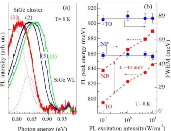
In contrast to MBE grown samples, chemical vapour deposition (CVD) growth of 3D Si/SiGe NSs does not pro-vide precise control over the atomic composition, and can produce more Si/SiGe interdiffusion at heterointerfaces [5]. This is reflected in PL spectra, where no fine structure has been found. However, the broad and asymmetric PL peak is well fitted by two Gaussian bands, often identified as the NP and TO phonon lines [12] and separated by an energy of ~43 meV, which is close to the energy of characteristic SiGe phonons (see Fig. 1). Thus, there is at least a qualita-tive similarity between PL spectra in MBE and CVD
grown 3D Si/SiGe NSs. The PL efficiencies in MBE and CVD grown samples are comparable (≥1% at low excita-tion intensity). The same sub-linear (close to square root) dependence on excitation intensity (on a log-log plot) for PL associated with Ge-rich SiGe clusters has been found in nearly all 3D Si/SiGe NSs grown by both CVD and MBE [13].
Figure 1 (a) Normalized PL spectra in CVD grown Si/SiGe 3D
NSs showing the PL spectral shift to higher photon energy under increasing excitation intensity. Each spectrum can be fitted with two (NP and TO) Gaussian spectral bands, as shown, for example, by the dashed lines under trace (1). (b) Summary of PL spectra changes as a function of excitation intensity.
The PL spectra in 3D Si/SiGe NSs, which is similar to that in III-V quantum wells with type II energy band alignment, exhibit a blue shift as the excitation intensity increases. This effect is found in both MBE and CVD grown samples. Figure 1 shows PL spectra in a CVD grown sample measured under different excitation intensi-ties. At the lowest excitation intensity used (0.1 W/cm2), the PL peaks at ~0.8 eV. With increasing excitation inten-sity, a continuous almost-parallel PL blue shift of 30–40 meV per decade of excitation intensity increase is observed. At an excitation intensity of 10 W/cm2, the PL peak reaches ~0.92 eV. Under photo-excitation of 1–10 kW/cm2, the low energy part of the PL spectrum does not shift fur-ther, while the high energy part continues shifting towards higher energy. A modified Arrhenius plot of the normal-ized integrated PL intensity as a function of temperature for the different excitation intensities can be fitted with two thermal quenching activation energies E1 and E2 (Fig. 2).
In all measurements of all samples, the PL thermal quench-ing activation energy Ε1~15 meV and is independent of excitation intensity. In contrast, the activation energy E2
depends significantly on the excitation intensity: the PL temperature dependence shows a step-like behavior, and E2
increases dramatically from ~120 to 340 meV as the exci-tation intensity increases from 0.1 to 10 W/cm2.
2872 D. J. Lockwood et al.: Self-assembled Si-Ge nanostructures for CMOS compatible light emitters
© Her Majesty the Queen in Right of Canada [2011]. Reproduced with the permission of the Minister of Industry www.pss-c.com
physica
p s s
statussolidi
c
Figure 2 Typical integrated PL intensity for CVD grown
sam-ples as a function of the reciprocal temperature measured under different excitation intensities, as indicated. The activation ener-gies obtained from fits (lines) to the data (points) are also given.
The PL dynamics under pulsed laser excitation reveal important information regarding the carrier recombination mechanism. Figure 3 shows the normalized low-temperature PL decays collected from a CVD grown Si/SiGe 3D sample. The initial PL decay is fast, close to the resolution of our detection system (<20 ns). The longer-lived PL shows a strong dependence on the detec-tion photon energy: the PL lifetime at photon energies be-low 0.8 eV is found to be ~20 µs and then drastically de-creases to ~200 ns for the PL measured at 0.89 eV. More complicated and even faster (~10-7 s) decays are observed at very high excitation intensities [14].
0 10 20 10-4 10-3 10-2 10-1 100 T = 4.4 K 0.89 eV 0.86 eV 0.83 eV 0.77 eV P L I n te ns ity ( ar b . units ) Time (μs)
Figure 3 Low temperature PL dynamics for a CVD grown
sam-ple measured at the indicated photon energies using a ~6 ns exci-tation pulse.
3 Carrier recombination In discussing carrier re-combination in Si/SiGe NSs, we focus on MBE and CVD grown samples with an average Ge atomic composition ~50%. These samples show the highest observed PL quan-tum efficiency with a PL peak wavelength close to 1.5-1.6 μm. The PL spectral distribution extending well below the bandgap of pure Ge and the extremely long carrier
radia-tive lifetime of ~10 ms [11], as well as the ~30 meV per decade PL spectral shift toward higher photon energies as the excitation intensity increases, point out strong similari-ties between the PL in 3D Si/SiGe NSs and the PL in III-V quantum wells with type II energy band alignment [15]. Generally, a type II energy band alignment at the hetero-interface is a strong disadvantage for light emitting devices due to a weak overlap between spatially separated electron and hole wave functions. In reality, however, the critical limitation in the efficiency of light-emitting structures is rather the presence of competing non-radiative recombina-tion channels for excess electrons and holes. The most im-portant non-radiative mechanism is carrier recombination via defects, especially hetero-interface structural defects such as propagating dislocations and dislocation com-plexes. The 3D Si/SiGe NSs investigated here show an al-most undetectable density of dislocations. Thus, at low ex-citation intensities, we find a high quantum efficiency of PL with photon energy < 0.9 eV, which is associated with carrier recombination in the vicinity of SiGe clusters.
It has already been suggested that SiGe Stranski-Krastanov (S-K) clusters with a small (3–5 nm) height and ~10:1 base-height aspect ratio can be modeled as NSs with a type II energy band alignment and possible SiGe cluster valence-band energy quantization in the direction of growth [10]. Strained Si and Si-rich SiGe alloy regions near the base of the clusters (also called SiGe wetting lay-ers) also need to be considered. Including the effect of strain, the observed PL bands at 0.916 and 0.972 eV indi-cate a composition of the Si1-xGex transition region, which
is located near the bottom of the Ge/Si pyramid-like clus-ters, to be close to x = 0.2, and this conclusion is supported by recent direct analytical TEM measurements [16].
It has also been proposed that the broad PL band with peak energy ~0.8–0.9 eV is due to the recombination of carriers localized in the Ge-richest areas of the clusters, which is close to the center of “pancake” shaped SiGe clusters [16]. We suggest that at the lowest excitation in-tensity, the PL arises from electron-hole recombination be-tween holes localized in the Ge-richest regions of the clus-ter and electrons localized in the strained SiGe alloy region near the cluster base. This immediately explains the exten-sion of the observed PL spectrum below the pure Ge band-gap energy.
The observed excitation-independent PL thermal quenching activation energy of ~15 meV is close to the ex-citon binding energy in SiGe alloys and Si/SiGe superlat-tices. Thus we conclude that one of the mechanisms of PL thermal quenching is the thermal dissociation of excitons. The activation energy of ~15 meV can therefore be associ-ated with exciton localization on specific regions of the clusters associated with variations of the SiGe composition. Hence, the non-uniform SiGe cluster composition and, perhaps, variations in SiGe cluster size and shape could be responsible for the observed relatively broad PL spectra.
Using the model discussed above of type II energy band alignment at the Si/SiGe heterointerface, we focus
Phys. Status Solidi C 8, No. 9 (2011) 2873
www.pss-c.com © Her Majesty the Queen in Right of Canada [2011]. Reproduced with the permission of the Minister of Industry
Invited Article
next on non-radiative carrier recombination and the differ-ent mechanisms of electron-hole separation. Electron transport in 3D Si/SiGe NSs is limited by a small (≤10–15 meV) conduction band energy barrier and SiGe composi-tional disorder [17]. Thus, the PL thermal quenching acti-vation energy of ~15 meV could also be associated with a small conduction band energy barrier for electrons in Si/SiGe 3D NSs.
In contrast to a low energy barrier for electrons, hole diffusion in 3D Si/SiGe multilayer NSs with a high Ge content is controlled by large (>100 meV) valence band energy barriers at Si/SiGe heterointerfaces. In this system, we consider two major mechanisms of hole transport: hole tunneling and hole thermionic emission. Hole tunneling in 3D Si/SiGe NSs with thin (5–7 nm) Si separating layers and nearly perfect SiGe cluster vertical self-alignment could be very efficient. These NSs are usually grown by MBE and exhibit a PL thermal quenching activation en-ergy of ~60 meV. The same PL thermal quenching activa-tion energy is found in our CVD-grown samples with 7.5 nm thick Si separating layers for the lowest excitation in-tensity. We suggest that in 3D Si/SiGe multilayer NSs with thin Si layers at low excitation intensity, the electron-hole separation and non-radiative carrier recombination are mainly controlled by hole tunneling between SiGe clusters. Due to significant variations in SiGe cluster size, shape and chemical composition, the process of hole tunneling could be assisted by phonon emission and/or absorption [13]. Therefore, the observed PL thermal quenching activa-tion energy is close to the Si TO phonon energy. In 3D Si/SiGe multilayer samples with 20 nm thick Si layers, where SiGe cluster vertical self-alignment is practically absent [5, 16], the probability of hole tunneling is reduced, and hole thermionic emission over the Si/SiGe hetero-interface barrier is playing a bigger role. Thus, in these samples the PL thermal quenching activation energy is ex-pected to be greater, as has been found in our experiments .
In this simple model, efficient hole tunneling between adjacent SiGe nanoclusters requires not only reasonably low and thin Si barriers but also a low carrier concentration (i.e., a large enough number of empty adjacent SiGe clus-ters). By increasing the photo-excitation intensity (i.e., the number of photogenerated carriers), hole tunneling can ef-fectively be suppressed since fewer empty adjacent SiGe clusters can be found. At high excitation intensity, assum-ing a negligible value of the conduction band offset com-pared to that in the valence band and a nearly pure Ge composition in the SiGe cluster core, the maximum antici-pated PL thermal quenching activation energy should be ~400 meV. This value sets the upper limit of the activation energy of PL intensity thermal quenching in 3D SiGe mul-tilayer NSs, and it is close to the activation energy of E2~340 meV that has been found under the highest excita-tion intensity.
The same model also explains the experimentally ob-served strong decrease in carrier radiative lifetime (~100 times) as the detection photon energy increases from 0.77
to 0.89 eV (Fig. 3). Under a low level of excitation inten-sity, holes are localized within the Ge-rich core of SiGe clusters, and the hole wave function does not penetrate into the Si barriers. Thus, in this quasi-type II energy band alignment, electron and hole wave functions do not overlap, causing a long carrier radiative lifetime. Under high level excitation, holes occupying the excited energy states in small size SiGe clusters, as well as holes leaking into the SiGe wetting layer with a lower Ge concentration, have their wave function significantly extended into the Si bar-riers. Therefore, a stronger overlap between electron and hole wave functions is responsible for a shorter radiative lifetime, i.e., a higher PL quantum efficiency at greater photon energy. Thus, this explanation is consistent with both, the decrease of the PL decay time at greater photon energy and the PL spectral blue shift as excitation intensity increases.
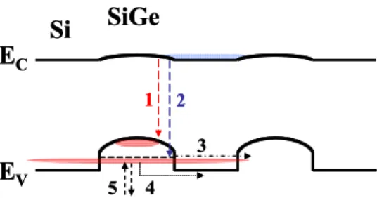
Figure 4 depicts the anticipated quasi-type II energy band alignment at Si/SiGe heterointerfaces, where a grad-ual increase of Ge concentration toward the SiGe cluster core has recently been experimentally verified [5, 16]. It also shows five major processes controlling electron-hole recombination in 3D Si/SiGe NSs with a Ge-rich core:
(1) radiative recombination between electrons localized at the Si/SiGe heterointerface and holes localized within the Ge-rich core of a SiGe cluster—this slow recombina-tion is associated with the lower photon energy part of the PL band;
(2) radiative recombination between electrons localized at the Si/SiGe heterointerface and holes localized in ex-cited states in small-size SiGe clusters as well as holes leaking into the Si-rich outer part of the cluster or/and SiGe wetting layer—this faster carrier recombination channel is responsible for the higher photon energy part of the PL spectrum;
(3) non-radiative carrier recombination due to electron-hole separation via electron-hole tunneling in Si/SiGe NS samples with thin (<10 nm) Si barriers;
(4) non-radiative carrier recombination due to electron-hole separation via electron-hole thermionic emission in samples with thicker (>15–20 nm) Si barriers;
(5) non-radiative carrier recombination due to Auger processes.
It has been pointed out that possible transformations of hole energy spectra due to quantization and/or strain might dramatically increase the rate of non-radiative Auger re-combination in SiGe quantum wells by more than 100 times [18]. Thus, the ‘Auger limit’ in Si/SiGe NSs could be considerably lower compared to that in bulk Si and Ge. On the other hand, the Auger process competes with radia-tive processes, and their characteristic lifetimes are ~10-3 s in bulk Si and Ge and just ~10-7 s in the high-photon-energy part of the PL spectra in 3D Si/SiGe NSs [14]. Therefore, more work needs to be done to understand the important details of Auger processes in Si/SiGe NSs.
Figure 4 also reflects a continuous change in the Ge atomic concentration by a gradually increasing energy
2874 D. J. Lockwood et al.: Self-assembled Si-Ge nanostructures for CMOS compatible light emitters
© Her Majesty the Queen in Right of Canada [2011]. Reproduced with the permission of the Minister of Industry www.pss-c.com
physica
p s s
statussolidi
c
band gap from the cluster center toward the cluster edge and SiGe wetting layer where the Ge atomic concentration is estimated to be ~20%. The proposed energy band dia-gram and carrier recombination/diffusion mechanisms ex-plain the experimental observations of (i) the PL spectral blue shift under increasing excitation intensity; (ii) the dramatic (~100 times) decrease in carrier radiative lifetime measured at photon energies from 0.77 to 0.89 eV; and (iii) the unusual PL intensity temperature dependence, which shows a different PL thermal quenching activation energy at different excitation intensities. This schematic represen-tation also points out that moderate excirepresen-tation intensity changes the overlap of electron-hole wave functions and allows a faster carrier radiative recombination. In other words, the type II energy band alignment at the Si/SiGe hetero-interface can effectively be replaced by the “dy-namic type I” alignment, where the electron and hole spa-tial separation no longer controls the recombination rate and the quantum efficiency of PL and EL.
E
CE
VSi
SiGe
1 2 3 4 5E
CE
VSi
SiGe
1 2 3 4 5Figure 4 Schematic of the Si/SiGe cluster multilayer energy
band diagram with different electronic transitions: 1 - slow elec-tron-hole recombination due to spatial separation and a weak wave function overlap; 2 - a faster recombination, presumably in-volving holes at excited energy states in SiGe clusters; 3 - hole diffusion due to cluster-to-cluster tunneling; 4 - hole diffusion due to thermionic processes; and 5 - Auger hole excitation with possible charge transfer.
4 Conclusion Comprehensive experimental studies of the light-emitting properties of 3D Si/SiGe NSs show that these nanostructures emit light at the technologically important 1.3–1.6 μm wavelength region. The highest PL (and EL) quantum efficiency is found in SiGe clusters with a ~50% Ge composition near the cluster core. Using time resolved PL measurements, it has been found that within the broad PL band, the part of the PL spectra at higher pho-ton energies exhibits a ~100 times faster radiative transi-tion, which is explained by a proposed model where radia-tive recombination occurs between holes occupying ex-cited states in SiGe clusters and electrons mostly localized at Si/SiGe interfaces. This fast PL is less susceptible to Auger-induced intensity saturation as the excitation inten-sity increases. In addition, this PL exhibits an improved in-tensity temperature dependence: the PL (and EL) can eas-ily be extended up to room temperature. These experimen-tal observations suggest that by controlling and modifying the composition of Ge-rich SiGe clusters (and possibly
other types of Si/SiGe 2D and 3D NSs) it is possible to fabricate a more efficient SiGe light-emitting device. De-spite the challenges associated with their integration into the traditional CMOS environment, the proven compatibil-ity between Si/SiGe and conventional CMOS technology suggests that this task is not an impossible one.
Acknowledgements We acknowledge the invaluable
con-tributions from our many collaborators and especially B. Kame-nev, J.-M. Baribeau, X. Wu, and T. Kamins. We thank US Na-tional Science Foundation, Intel Corporation, Semiconductor Re-search Corporation, and Foundation at NJIT for financial support.
References
[1] L. Tsybeskov, D. J. Lockwood, and M. Ichikawa, Proc. IEEE 97, 1161 (2009).
[2] L. Pavesi and D. J. Lockwood (eds.), Silicon Photonics (Springer, Berlin, 2004).
[3] D. J. Lockwood and L.Paveis (eds.), Silicon Photonics II (Springer, Berlin, 2010).
[4] D.J. Lockwood (ed.), Light Emission in Silicon: From Phys-ics to Devices (Academic Press, San Diego, 1998).
[5] J.-M. Baribeau, X. Wu, N. L. Rowell, and D. J. Lockwood, J. Phys.: Condens. Matter 18, R139 (2006).
[6] R. Apetz, L. Vescan, A. Hartmann, C. Dieker, and H. Lüth, Appl. Phys. Lett. 66, 445 (1995).
[7] P. Schittenhelm, M. Gail, J. Brunner, J. F. Nützel, and G. Abstreiter, Appl. Phys. Lett. 67, 1292 (1995).
[8] O. G. Schmidt, C. Lange, and K. Eberl, Appl. Phys. Lett. 75, 1905 (1999).
[9] B. V. Kamenev, L. Tsybeskov, J.-M. Baribeau, and D. J. Lockwood, Appl. Phys. Lett. 84, 1293 (2004).
[10] M. El Kurdi, S. Sauvage, G. Fishman, and P. Boucaud, Phys. Rev. B 73, 195327 (2006) and references therein.
[11] B. V. Kamenev, L. Tsybeskov, J.-M. Baribeau, and D. J. Lockwood, Phys. Rev. B 72, 193306 (2005).
[12] B. V. Kamenev, H. Grebel, L. Tsybeskov, T. I. Kamins, R. S. Williams, J.-M. Baribeau, and D. J. Lockwood, Appl. Phys. Lett. 83, 5035 (2003).
[13] B. V. Kamenev, E.-K. Lee, H.-Y. Chang, H. Han, H. Grebel, L. Tsybeskov, and T. I. Kamins, Appl. Phys. Lett. 89, 153106 (2006).
[14] E.-K. Lee, D.J. Lockwood, J.-M. Baribeau, A.M.
Bratkovsky, T.I. Kamins, and L. Tsybeskov, Phys. Rev. B
79, 233307 (2009); Phys. Rev. B 80, 049904 (2009).
[15] J. Hu, X. G. Xu, J. A. H. Stotz, S. P. Watkins, A. E. Curzon, M. L. W. Thewalt, N. Matine, and C. R. Bolognesi, Appl. Phys. Lett. 73, 2799 (1998).
[16] D. J. Lockwood, X. Wu, and J.-M. Baribeau, IEEE Trans. Nanotechnol. 6, 245 (2007).
[17] T. Baier, U. Mantz, K. Thonke, R. Sauer, F. Schäffler, and H.-J. Herzog, Phys. Rev. B 50, 15191 (1994).
[18] C. J. Williams, E. Corbin, M. Jaros, D.C. Herbert, Physica B: Condens. Matter 254, 240 (1998).