Publisher’s version / Version de l'éditeur:
Vous avez des questions? Nous pouvons vous aider. Pour communiquer directement avec un auteur, consultez la première page de la revue dans laquelle son article a été publié afin de trouver ses coordonnées. Si vous n’arrivez pas à les repérer, communiquez avec nous à [email protected].
Questions? Contact the NRC Publications Archive team at
[email protected]. If you wish to email the authors directly, please see the first page of the publication for their contact information.
https://publications-cnrc.canada.ca/fra/droits
L’accès à ce site Web et l’utilisation de son contenu sont assujettis aux conditions présentées dans le site LISEZ CES CONDITIONS ATTENTIVEMENT AVANT D’UTILISER CE SITE WEB.
Langmuir, 23, 4, pp. 1612-1614, 2007-02-01
READ THESE TERMS AND CONDITIONS CAREFULLY BEFORE USING THIS WEBSITE. https://nrc-publications.canada.ca/eng/copyright
NRC Publications Archive Record / Notice des Archives des publications du CNRC :
https://nrc-publications.canada.ca/eng/view/object/?id=db86dae3-0d2c-439f-97c0-abc036993a55
https://publications-cnrc.canada.ca/fra/voir/objet/?id=db86dae3-0d2c-439f-97c0-abc036993a55
NRC Publications Archive
Archives des publications du CNRC
This publication could be one of several versions: author’s original, accepted manuscript or the publisher’s version. / La version de cette publication peut être l’une des suivantes : la version prépublication de l’auteur, la version acceptée du manuscrit ou la version de l’éditeur.
For the publisher’s version, please access the DOI link below./ Pour consulter la version de l’éditeur, utilisez le lien DOI ci-dessous.
https://doi.org/10.1021/la0629274
Access and use of this website and the material on it are subject to the Terms and Conditions set forth at
Ordered CdSe nanoparticles within self-assembled block copolymer
domains on surfaces
Ordered CdSe Nanoparticles within Self-Assembled Block
Copolymer Domains on Surfaces
Shan Zou,
†Rui Hong,
‡Todd Emrick,
‡and Gilbert C. Walker*
,†Department of Chemistry and Institute for Optical Sciences, UniVersity of Toronto, 80 St. George Street, Toronto, Ontario M5S 3H6, Canada, and Department of Polymer Science and Engineering, UniVersity of
Massachusetts, 120 GoVernors DriVe, Amherst, Massachusetts 01003 ReceiVed October 5, 2006. In Final Form: January 10, 2007
Hierarchical, high-density, ordered patterns were fabricated on Si substrates by self-assembly of CdSe nanoparticles within ∼20-nm-thick diblock copolymer films in a controlled manner. Surface-modified CdSe nanoparticles formed well-defined structures within microphase-separated polystyrene-b-poly(2-vinylpyridine) (PS-b-P2VP) domains. Trioctylphosphine oxide (TOPO)-coated CdSe nanoparticles were incorporated into PS domains and polyethylene glycol-coated CdSe nanoparticles were located primarily in the P2VP domains. Nearly close-packed CdSe nanoparticles were clearly identified within the highly ordered patterns on Si substrates by scanning electron microscopy (SEM). Contact angle measurements together with SEM results indicate that TOPO-CdSe nanoparticles were partially placed at the air/copolymer interface.
Introduction
Engineering the self-assembly of inorganic nanoparticles within block copolymer nanodomains is useful for the design of periodic structures to form materials with enhanced mechanical strength as well as to achieve unique optical, electronic, and magnetic properties on the nanometer scale. The technological relevance of these nanoscale materials is linked to a fundamental understanding of the structural characteristics to afford a reliable prediction of, for example, the photonic properties needed to tailor the materials for various applications. Several experimental processes and theoretical models have been developed for the incorporation of inorganic nanoparticles into polymeric nano-structures.1-10 On the basis of theoretical predictions of the
cooperative self-assembly of nanoparticles and block copoly-mers,11-13 Bockstaller et al.6demonstrated pattern formation
using mixtures of hydrophobic nanoparticles and block copoly-mers. More recently, the work of Russell and co-workers7showed
that the pattern of block-copolymer domains in films could be influenced by nanoparticles. In addition, Kramer and co-workers8
showed that polymer-grafted Au nanoparticles can be located either inside the block-copolymer domains or at the interface of
the two block-copolymer domains. Precise control of the position of the nanoparticles within block-copolymer films is important for developing organized hybrid materials to obtain practical functionality. In many of those applications, including the above-mentioned photonic band gap devices, nanostructured solar cells, magnetic storage media, and biomedical devices, it is important to fabricate highly ordered patterns of nanoparticles on surfaces. Several conventional fabrication methods, including standard photolithography,14,15electron beam lithography,16,17and other
lithographic techniques,18-20have been employed to generate
well-organized nanostructures. However, these approaches are often sophisticated and limited in terms of minimum achievable feature sizes.
In this letter, we report a study that set out to examine whether nanoparticles could be loaded heavily within domains of a phase-segregated diblock copolymer film on a solid surface such that the particles would be close-packed on one length scale while the diblock polymer remained cleanly phase-separated on a second length scale. We demonstrate the formation of highly ordered hierarchical structures on solid surfaces by controlling the surface hydrophobicity of nanoparticles within ∼20-nm-thick diblock copolymer films. High-resolution scanning electron microscopy (SEM) and transmission electron microscopy (TEM) images were made of the CdSe-diblock copolymer hybrid films and were used to identify individual CdSe nanoparticles within the highly ordered patterns on solid substrates in which the spatial location of the nanoparticles was determined by their surface ligands. Moreover, contact angle experiments supported the determination of the location of TOPO-CdSe nanoparticles.
Diblock copolymer poly(styrene-b-2 vinyl pyridine) (PS-b-P2VP) (Mw(PS) ) 52.4 kg/mol, Mw(P2VP) ) 28.1 kg/mol, PDI
)1.11, Polymer Source Inc., Canada) and tri-n-octylphosphine oxide (TOPO)-coated CdSe nanoparticles (TOPO-CdSe, core diameter 4 nm, Evident Technologies, NY) were used in our
* Corresponding author. E-mail: [email protected].
†University of Toronto. ‡University of Massachusetts.
(1) Lauter-Pasyuk, V.; Lauter, H. J.; Ausserre, D.; Gallot, Y.; Cabuil, V.; Kornilov, E. I.; Hamdoun, B. Phys. B. 1997, 241, 1092-1094.
(2) Bronstein, L. H.; Sidorov, S. N.; Valetsky, P. M.; Hartmann, J.; Colfen, H.; Antonietti, M. Langmuir 1999, 15, 6256-6262.
(3) Tsutsumi, K. F., Y.; Hirokawa, Y.; Hashimoto, T. Langmuir 1999, 15, 5200-5203.
(4) Horiuchi, S.; Sarwar, M. I.; Nakao, Y. AdV. Mater. 2000, 12, 1507-1511. (5) Lopes, W. A.; Jaeger, H. M. Nature 2001, 414, 735-738.
(6) Bockstaller, M. R.; Lapetnikov, Y.; Margel, S.; Thomas, E. L. J. Am.
Chem. Soc. 2003, 125, 5276-5277.
(7) Lin, Y.; Boker, A.; He, J. B.; Sill, K.; Xiang, H. Q.; Abetz, C.; Li, X. F.; Wang, J.; Emrick, T.; Long, S.; Wang, Q.; Balazs, A.; Russell, T. P. Nature 2005,
434, 55-59.
(8) Chiu, J. J.; Kim, B. J.; Kramer, E. J.; Pine, D. J. J. Am. Chem. Soc. 2005,
127, 5036-5037.
(9) Aizawa, M.; Buriak, J. M. J. Am. Chem. Soc. 2006, 128, 5877-5886. (10) Sohn, B. H.; Choi, J. M.; Yoo, S. I.; Yun, S. H.; Zin, W. C.; Jung, J. C.; Kanehara, M.; Hirata, T.; Teranishi, T. J. Am. Chem. Soc. 2003, 125, 6368-6369. (11) Huh, J.; Ginzburg, V. V.; Balazs, A. C. Macromolecules 2000, 33, 8085-8096.
(12) Ginzburg, V. V.; Gibbons, C.; Qiu, F.; Peng, G. W.; Balazs, A. C.
Macromolecules 2000, 33, 6140-6147.
(13) Thompson, R. B.; Ginzburg, V. V.; Matsen, M. W.; Balazs, A. C. Science
2001, 292, 2469-2472.
(14) Wallraff, G. M.; Hinsberg, W. D. Chem. ReV. 1999, 99, 1801-1821. (15) Shipway, A. N.; Katz, E.; Willner, I. Chem. Phys. Chem. 2000, 1, 18-52. (16) Ito, T.; Okazaki, S. Nature 2000, 406, 1027-1031.
(17) Wong, W. H.; Zhou, J.; Pun, E. Y. B. Appl. Phys. Lett. 2001, 78, 2110-2112.
(18) Haynes, C. L.; Van, Duyne, R. P. J. Phys. Chem. B 2001, 105, 5599-5611.
(19) Bullen, H. A.; Garrett, S. J. Nano Lett. 2002, 2, 739-745.
(20) Garcia, R.; Martinez, R. V.; Martinez, J. Chem. ReV. 2006, 35, 29-38.
1612 Langmuir 2007, 23,1612-1614
10.1021/la0629274 CCC: $37.00 © 2007 American Chemical Society Published on Web 01/23/2007
study. Films with thicknesses of 20 ( 2 nm were prepared by spin coating toluene solutions of a mixture of 0.3 wt % PS-b-P2VP and 0.05 wt % TOPO-CdSe on silicon substrates. Prior to use, Si wafers were immersed in freshly prepared piranha solution (3:1 v/v H2SO4/H2O2) for 10 min. Then they were rinsed
with excess Milli-Q water, acetone, and toluene and immediately dried in a nitrogen stream. (Piranha solution should be handled
with extreme caution. It has been reported to detonate unexpectedly.)Before and after the TOPO-CdSe/copolymer films were annealed in saturated dichloromethane vapor for 4 h at 25
°C,21the samples were kept under vacuum for 16-20 h to remove
the solvent. In agreement with the literature,7we found that
solutions of TOPO-CdSe nanoparticles and the block copolymer were stable at room temperature; aggregation caused by ligand exchange was not observed.
Atomic force microscopy (AFM) height and phase images of an annealed TOPO-CdSe/PS-P2VP film with a thickness of ∼20 nm are shown in Figure 1. AFM measurements were made using a Digital Instruments Dimension 5000 AFM (DI/Veeco, Santa Barbara, CA) operated in tapping mode using silicon probes (Mikromasch, resonance frequencies in the range of 175-350 kHz, free amplitude 20-25 nm). Before annealing, the mixed nanoparticle/copolymer films presented quasi-hexagonal micellar patterns on Si substrates (Supporting Information Figure S1).22,23
In Figure 1A, a highly ordered array of microphase-separated domains of P2VP in a PS matrix is observed for the annealed films on Si substrates. Using Fourier transformation of the AFM images (Figure 1A inset), the lattice spacing of the hexagonal packing domains was found to be 40 ( 1 nm for the TOPO-CdSe/copolymer films. The ordered structure is similar to that of the annealed pure PS-b-P2VP films on Si surfaces (Supporting Information Figure S2). However, the pronounced increase in height and phase contrast indicates that the hard nanoparticles were incorporated into the PS phase (Figure 1B, bright areas).7
Figure 2 shows scanning electron microscopy (SEM, S-5200, Hitachi microscope operated at 5 kV) images of CH2Cl2
vapor-annealed films on silicon wafers. First, the Figure illustrates a significant degree of regular diblock phase segregation. PS domains are about 40 nm in diameter. The second important observation is that TOPO-CdSe nanoparticles with diameters of 4 to 5 nm are distinctly identified within the PS domains. This location of TOPO-CdSe particles is expected as a result of the hydrophobic modification of TOPO groups on the surface of
CdSe particles, which increase the favorable molecular interac-tions between PS blocks and the nanoparticles, in preference to P2VP/TOPO-CdSe nanoparticle) or PS/P2VP (block-block) interactions.
As can be seen in the inset to Figure 2 (lower right image), the CdSe particles are nearly close-packed and exhibit a high degree of local order. A pairwise correlation plot for these particles can be found in Supporting Information. As others have shown, a low degree of particle loading does not interfere with the diblock pattern formation (Figure S3).8However, Figure 2 shows the
remarkable result that greater than 75% lateral loading of particles into single domain types can be accomplished while retaining the majority of the diblock-induced range order. Some long-range-order defects were observed in the nanoparticle/copolymer mixed films. Further vapor annealing did not improve the ordering of the particles within the PS domains but resulted instead in the collapse of the ∼20-nm-thick films. This indicates that such films are not stable for long periods of vapor annealing. Therefore, the CdSe particles may not obtain sufficient mobility to form ideal hexagonal structures on surfaces.
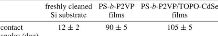
Advancing contact angles of freshly treated Si substrates, pure diblock copolymer films, and highly ordered nanoparticles/ copolymer pattern films were measured with water at room temperature (Table 1). Pure copolymer films showed hydrophobic behavior due to the preferential adsorption of the P2VP blocks to the hydrophilic silicon surfaces with most of the PS chains staying close to the air interface.24,25After adding the
TOPO-CdSe nanoparticles to the PS-b-P2VP copolymer, the patterned films showed even higher hydrophobicity. This is reasonable if the alkyl chains of TOPO molecules are exposed to the air-polymer interfaces. Consider that the adsorption energy of a nanoparticle at an air-polymer interface is given by Ea )
πR2γpoly/air(1 - |(γCdSe/poly- γCdSe/air)/γpoly/air|), where R is the
radius of the nanoparticles and γpoly/air, γCdSe/poly, and γCdSe/airare
the interfacial tensions of polymer-air, nanoparticles-polymer, and nanoparticles-air, respectively. Here, R ) 2.5 nm, γpoly/air
(21) Kim, S. H.; Misner, M. J.; Xu, T.; Kimura, M.; Russell, T. P. AdV. Mater.
2004, 16, 226-231.
(22) Li, Z.; Zhao, W.; Liu, Y.; Rafailovich, M. H.; Sokolov, J.; Khougaz, K.; Eisenberg, A.; Lennox, R. B.; Krausch, G. J. Am. Chem. Soc. 1996, 118, 10892-10893.
(23) Li, X.; Lau, K. H. A.; Kim, D. H.; Knoll, W. Langmuir 2005, 21, 5212-5217.
(24) Minko, S.; Patil, S.; Datsyuk, V.; Simon, F.; Eichhorn, K. J.; Motornov, M.; Usov, D.; Tokarev, I.; Stamm, M. Langmuir 2002, 18, 289-296.
(25) Adao, M.; Saramago, B. J. V.; Fernandes, A. C. J. Colloid Interface Sci.
1999, 217, 94-106. Figure 1. AFM (A) height and (B) phase images of a CH2Cl2
vapor-annealed TOPO-CdSe/PS-b-P2VP film on a Si substrate. Image size: 2500 nm × 2500 nm. Z range: 10 nm, 30°. The inset in A is a Fourier transformation of the height image.
Figure 2. SEM micrographs of an annealed PS-b-P2VP/TOPO-CdSe film on Si at 5 kV acceleration voltage. The inset scheme shows the packing of the nanoparticles.
Table 1. Advancing Water Contact Angles Measured on Si Substrates, PS-b-P2VP Films, and PS-b-P2VP/TOPO-CdSe
Ordered Pattern Films
freshly cleaned Si substrate PS-b-P2VP films PS-b-P2VP/TOPO-CdSe films contact angles (deg) 12 ( 2 90 ( 5 105 ( 5
)36 mN/m,26
γCdSe/poly≈25 mN/m,27and γCdSe/air)33 mN/m,7
which gives Ea ≈ 100kBT. Therefore, it is expected that the
particles should be found at the polymer-air interface. The clearly resolved CdSe nanoparticles in SEM images and the increasing hydrophobicity of nanoparticles/polymer mixture films indicate that the TOPO-CdSe nanoparticles were at least partially located at air-polymer interface.
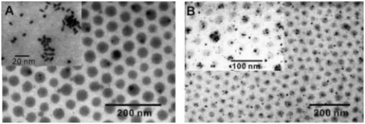
Further reference samples of hydrophilic coated CdSe nano-particles and PS-b-P2VP mixed films were analyzed by TEM. Polyethylene glycol-coated CdSe nanoparticles28(PEG-CdSe)
with diameters of ∼5 nm (Figure 3A inset) were cast from 0.05 mg/mL chloroform solution on carbon-supported TEM grids. Figure 3A shows a typical TEM micrograph of spin-coated films prepared from 0.025 mg/mL PEG-CdSe and a 0.3 wt % PS-b-P2VP chloroform solution on carbon-supported TEM grids. After vapor annealing in CH2Cl2for 4 h and drying at 70°C for 16-20
h, a well-defined micropattern structure of diblock copolymer was detected over a large area without the prominent presence
of CdSe particles. Dark domains in Figure 3A represent P2VP domains in the PS matrix (bright area). Upon increasing the PEG-CdSe concentration to 0.25 mg/mL, the nanoparticles were mostly found in P2VP domains, as illustrated in the TEM micrographs shown in Figure 3B. Particles did not situate at phase boundaries apparently because of the strength of the favorable PEG-P2VP interaction.12
In summary, we have demonstrated the fabrication of highly ordered hierarchical structures on Si substrates using the self-assembly of CdSe nanoparticles within PS-b-P2VP diblock copolymer films in a controlled manner. TOPO-CdSe nanopar-ticles were incorporated into PS domains, and PEG-CdSe nanoparticles were located mostly in P2VP domains. Individual CdSe nanoparticles can be clearly identified within the highly ordered patterns on Si substrates. Low particle loading allows the diblock pattern to form unimpeded. Interestingly, at higher loading even in ranges where strong particle-particle packing forces come to bear, the longer length scale self-assembly of the diblock system was only slightly affected. Contact angle measurements together with SEM results indicate that TOPO-CdSe nanoparticles were partially placed at the air-copolymer interface.
Acknowledgment. The NSERC (312497), NIH (IR21EB003101-01), ONR (N00014-05-10765), ARO-MURI (W911NF-04-1-0191), Canada Research Chair Program, and NSF (CHE-0404579) are acknowledged for financial support.
Supporting Information Available: AFM images of neat copolymer and nanoparticles/copolymer films before annealing and a histogram of the nanoparticle center-to-center distance pairwise cor-relation plot. This material is available free of charge via the Internet at http://pubs.acs.org.
LA0629274
(26) Jones, R.; Richards, R. W. Polymers at Surfaces and Interfaces; Cambridge University Press: New York, 1999.
(27) Ferroni, E.; Gabrielli, G. J. Polym. Sci., Part B 1964, 2, 51-53. (28) Hong, R.; Fischer, N. O.; Verma, A.; Goodman, C. M.; Emrick, T.; Rotello, V. M. J. Am. Chem. Soc. 2004, 126, 739-743.
Figure 3. Bright field TEM images of (A) low and (B) high concentrations of PEG-CdSe in PEG-CdSe/PS-b-P2VP films. The inset in A shows the PEG-CdSe nanoparticles without polymer films.