CONTROLLED NUCLEATION AND GROWTH PROCESS FOR LARGE GRAINED POLYCRYSTALLINE SILICON PHOTOVOLTAICS
by
Dr. Stephen C. Danforth and
Dr. John S. Haggerty MIT-EL 82-028
MITLibraries
Document Services
Room 14-0551 77 Massachusetts Avenue Cambridge, MA 02139 Ph: 617.253.5668 Fax: 617.253.1690 Email: [email protected] http://libraries.mit.edu/docsDISCLAIMER OF QUALITY
Due to the
condition of
the original material, there
are unavoidable
flaws in this
reproduction. We have made every effort possible to
provide
you
with
the
best
copy available. If you
are dissatisfied with
this
product and
find
it
unusable, please
contact Document Services as
soon
as possible.
Thank
you.
This report contains poor gra-yscale reproduction and
is the best copy available.
Please note that pages 75-95 are an attachment to this
report (Van Gieson, Franklin D.)
ABSTRACT
Research has been conducted to develop a new means of producing large grained polycrystlline thin films for photovoltaic applications. The process is one of growth of controlled crystalline nuclei in an a-Si film. For this process to be practicle, we must develop a-Si films with crystallization behavior such that the rate of spontaneous crystallization (nucleation rate) is essentially zero at temperatures where the growth rates are > 104 A/min. Amorphous Si films, deposited on oxidized single crystal substrates by RF sputtering, E-beam evaporation, and CVD, have been examined. The
spontaneous crystallization behavior and the rates of nucleation and growth of crystals in the Si films have been evaluated using X-ray diffraction and TEM. The results show that microstructural features and impurities in the RF sputtered films result in very high nucleation rates and extremely low growth rates. The CVD films have high nucleation rates associated with the high deposition temperatures. The growth rates for Si crystallites into a-Si in the CVD films are only a factor of 20 below desired levels.
For process demonstration one requires a deposition process that will produce extremely high purity (- 101 8/cm3) a-Si films at low deposition temperatures. It remains to be seen if this can be done economically by E-beam or conventional CVD processes.
Table of Contents
page
Abstract
2
Table of Contents
3
List
of
Figures
5
List of Tables
7
List of Symbols
8
Acknowledgements
9
I.
Introduction
10
II.
Background
13
III.
Literature Review
16
A. Steady State Nucleation
16
B. Transient Nucleation
17
C.
Growth
19
1. Models
19
2. Rates and activation energies, pure a-Si
21
"3.
Impurity effects
23
4. Effect of a-Si density on growth
25
5. General expression
25
IV.
Description of Work
26
A.
Experimental Apparatus and Procedure
28
1. Substrate 28
2. Cleaning Procedure
29
3.
Deposition Processes
31
a.
Rf-sputtered films
31
b. Chemical Vapor Deposition (CVD)
31
Contenta
2a92
4. Annealing furnace and procedure
31
5. Transmission Electron Microscopy (TEM) 32
a. Specimen preparation
32
b. Artifacts
32
a. Interpretation of TEM results
33
V.
Results and Discussion
36
A. As-deposited silicon films
36
B. Determination of crystallinity
39
C. Rf-sputtered films
42
1. Nucleation rates
42
2. Growth in rf-sputtered films
44
a. Pinning by argon
50
b. Pinning at internal boundaries
51
D. Chemical Vapor Deposited (CVD)
films
52
1. Nucleation
52
2. Shape Anisotropy (CVD)
t
56
3. Growth in the CVD film
58
4.
Twins
62
E. Implications for the fabrication of large grain
63
polycrystalline films
VI.
Summary
and Conclusions
64
VII.
Suggestions for further
work
66
Appendix
1:
Crystallization temperatures for various a-Si films
67
Appendix 2: TEM sample preparation
68
Appendix 3: Correlation of density of crystallites apparent
70
in dark-field TEM to the actual density
List of Figures
Fiue
2age.
1. Differentially etched laser irradiated spot on
14
a-Si, after anneal
2. Nucleation rates versus temperature for vapor-deposited
18
a-Si
3. Silicon crystal structure
20
4. Growth rates versus temperature, pure a-Si
22
5. Growth rates versus temperature, impurity effects
24
6. TEM micrographs, rf-sputtered a-Si:
37
a. as-deposited
b.
3.5
hour anneal, 7240C
c. 7 hour anneal,
7240C
7. TEM micrographs, rf-sputtered a-Si:
38
a. 15 hour anneal, 724
0C
b. 16 hour anneal,
724
0C
8. TEM micrographs, Chemical Vapor Deposited (CVD)
a-Si:
40
a. 3 hour anneal, 551
0C
b.
5 hour anneal, 551
0C
c. 23 hour anneal, 551
0C
9. TEM micrographs, Chemical Vapor Deposited (CVD)
a-Si:
41
16 hour anneal, 812
0C
10. Nucleation behavior with time, rf-sputtered films at 7241C
43
11.
Crystallite size distributions, rf-sputtered films at 724cC
46
a.
3.5
hour anneal, 724
0C
b. 5 hour anneal, 724
0C
c. 7.5 hour anneal, 724
0C
12. Crystallite size distributions, rf-sputtered films at 724
0C
47
a. 9 hour anneal, 724C
b. 15 hour anneal,
724
0C
13. Mean sizes vs time, rf-sputtered film annealed at 7241C
49
14.
Nucleation behavior with time for CVD
films at 551
0C
54
15.
Axial ratio vs size for
CVD
films at
551
0C
57
Fimre
16. Crystallite
Major
Axis:
17. Crystallite Minor Axis:
size distributions, CYD
films
at 551
0C
a. 3 hour anneal, 551C
b.
5 hout anneal, 551
0C
a. 7 hour anneal, 551*C
d.
16 hour apieal, 551"C
e. 23 hour anneal, 551°c
size distributions, CVD films at 5510C
a. 3 hour anneal, 551
0C
b.
5 hour
anneal,
551*C
o.
7 hour anneal, 551
0C
d.
16 hour
anneal,
5511C
e.
23
holur
anneal, 551
0C
59
60
61
61
18. Mean crystallite sizes versus time, CVD films at 5510C19. Maximum observed crystallite size versus time, CVD films
7
List of Tables
1. Deposition Parameters
27
2. Annealing times and temperatures
27
3. Substrate Cleaning Procedure
30
4.
Nucleation rates, rf-sputtered (0S1-023) a-Si at 724
0C
45
List of Symbols
Sttitl Descriotion
5 Transformation-boundary thickness
AF Free energy difference per mole for phases
on the two sides of the boundary
AF ) G Free energy of activation for migration of the
transformation boundary
AG Gibbs free energy of a critical nucleus
Aag Activation energy for mass transport across
the transformation boundary
h Planck's Constant
I Nucleation rate
Ist Steady state nucleation rate
k Boltzmann's Constant
N Avagadro's number
R Ideal gas Constant
T Temperature
Ts Substrate temperature during deposition
t Time Transient time V Growth rate g Chemical potential x Distance
derivative (mathematical operation)
X Wavelength
-
~
--- inliliiY9
Acknowledgements
The author wishes to thank
Drs.
John Haggerty and Steve Danforth
whose guidance and support were instrumental in this research. I am
also indebted to Prof. Ken Russell for his
enthusiastic
and
instructive counsel in bringing this work to fruition. Finally, I
wish to thank the many collegues and members of the support staff
whose aid made this work possible.
Among these are Joe Hillman, Prof.
Hank Smith and
Michael Geiss.
Mr.
Hillman deposited the rf-sputtered
film and Prof. Smith and Mr. Geiss provided the CVD film used in
this
study.
I also wish to acknowledge the sponsor of this research, SERI
(Solar Energy Research Institute) and DOE (Department of Energy) which
provided financial support for this project.
I.
Introduction
Traditionally, single crystal silicon photovotaic cells have been used to provide electricity from large solar arrays. However, the
cost of these devices has limited their use principly to applications where alternative energy sources were impractical. DOE (Department of
Energy) estimates that the lowest possible cost for single crystal
1
solar cells is about $1.00/watt. This is 200 to 400% too high to be cost competitive with other energy sources. However, this cost
might be dramatically reduced if thin amorphous or polycrystalline silicon thin films on inexpensive substrates could be substituted for single crystal silicon substrates in solar cells. This could result in a 5000% reduction in the amount of ultra-high purity silicon required for these cells, greatly reducing the cost.
The difficulty is that solar cells made with amorphous and fine-grained polycrystalline silicon have lower photovoltaic conversion efficiencies than single crystal devices. The highest
3t tt
efficiency achieved for an amorphous cell is 6.5% at AM1 and 9.5% 4
at AM1 for a fine-grained polycrystalline silicon device. The typical
4
efficiency of a single crystal silicon device is 15% at AMI.
* These numbers depend on whether peak or average power demand is assumed, on the specific energy source, and on the location of the user.
** assuming that the single crystal device is 0.4 mm thick, that
cutting and polishing losses are 59% (Ref. 2) and that the
vapor-deposited film is 30 Am thick.
? for a hydrogenated amorphous silicon device.
tt
illumination equivalent to that of the sun after passing through 1 mile of atmosphere, or 930 W/m2 of radiant energy.These relative efficiencies arise from the low electron mobilities
through grain boundaries and in amorphous silicon due to electron
trapping by dangling bonds and other defects.
The costs associated with any large photovoltaic installation
dictate that a minimum conversion efficiency of 10-12% is required for
5
its economic viability. Rence the existing amorphous and
fine-grained polycrystalline silicon technologies are inadequate for
this application. An attractive alternative would be to create a
thin-film polycrystalline silioon device with grain sizes 10-100 times
4
the film thickness. This would minimize the interaction of grain
boundaries with electrns in a photovoltaic cell. 6
Ghosh calculated that a silicon photovoltaic cell using a 20 Am
thick film with- a 500 Am grain size could have a 10% efficiency.
However, the cost could be substantially lower than for a single
crystal device.
7
In a proposal developed at M.I.T., such a film would be created
by laser-irradiating small spots (< 10 urs diam.) on 1000 Am centers in
a 30 Am thick amorphous silicon film, to create crystalline nuclei
which subsequently would grow to impingement on anneal.
To do this,
conditions must be created under which nucleation can be controlled.
In the proposed process, nucleation in amorphous
silicon would be
controlled by annealing the laser-irradiated silicon film at a
SThese can be created by melting a thin surface layer of the
amorphous silicon film by nanosecond or longer laser pulses (Ref. 9).
** Recrystallization of silicon to achieve large grains is not
economic. The rate of grain boundary migration during
12
temperature
below
that for spontaneous
crystallization
of
the
as-deposited silicon film.
Examination
of annealed
amorphous
silicon
films
by
X-ray
diffraction
and
by
selective
etching
indicated
very small
characteristic grain sizes in all crystallized films,
independent
of
laser
processing.
However, neither of these techniques could provide
detailed information about
the crystallization
kinetics
in
these
films.
Therefore, a transmission electron microscope
(TEM)
investigation
was initiated to
determine the nature of the processes constraining
large-grain growth in these films.
The films investigated
were ones
believed
to
be
promising as
candidate materials for growing
large-grain polycrystalline silicon thin films by the above
process.
Nucleation
and growth
rates during the crystallization of amorphous
silicon were measured using the TEM.
The
chemistry
of
these films
was also investigated.
II. Background
A simple criterion for selecting an appropriate film deposition
method and parameters for this selective nucleation and growth
process is to chose a film with the maximum crystallization
temperature. The rationale was that we wished to maximize growth
rates at the crystalline spots (created with a laser) without having
this growth terminated by spontaneous crystallization in the a-Si
film. Spontaneous crystallization of a-Si was suppressed by annealing
the laser-irradiated films below the crystallization temperature of
the as-deposited film. The maximum anneal temperature, and hence, the
maximum growth rate at the (laser-created) crystalline spots is
determined by the crystallization temperature of the as-deposited film in this process.
X-ray diffraction studies of e-beam evaporated, rf-sputtered and
chemical vapor deposited (CYD) films were performed in conjunction
10 11
with Devaud
and
King.
These results suggested that rf-sputtered
amorphous silicon films, deposited with the substrate at T =400C,
have the highest crystallization temperature, of the samples studied,
(Appendix 1).
Growth of polycrystalline spots created with the laser* in this
rf-sputtered film was measured by differential etching (Stirl etch)
samples before and after annealing at 709 oC for 10 hours. The
crystallization temperature was 724 OC, for a 16 hour anneal. The
sample, after anneal and etch is shown in Figure 1. The inferred
* An argon laser (X=532 zm) was used. The pulse length was 114 ms
U) C $4 J r4 4 I4 '4- r-U)z I I 1 11 1 1 11 --1 -1 -1 --1 1-1 77 -- -.-.. -, -I I
-2
growth rate of this polycrystalline spot was 2.8x10 rm/sec at 709 oC. As demonstrated later (see Section III-C-2, Figure 3), this is at least several orders of magnitude lower than growth rates reported by earlier researchers for amorphous silicon deposited by evaporation, or created by ion-implantation.
X-ray line broadening also indicated that the grain sizes in all isothermally annealed amorphous silicon films (1200 nm thick) were no larger than 150 =s for there was no evidence of any spottiness in the diffraction rings.
In the initial stages of the transmission electron microscopy
(TEM) investigation of these films, e-beam evaporated, rf-sputtered and CVD deposited amorphous silicon films were considered for further study.
The e-beam evaporated films had two drawbacks relative to project interests. There were severe adhesion problems with these films on the oxidized single crystal silicon substrates. Although this could have been overcome, TEM examination of e-beam evaporated a-Si annealed at 701 oC revealed very irregular crystallites with lenticular or tree-like structures. Therefore, this film did not appear to be promising relative to the requirements of large-grain polycrystalline thin film development.
The CVD film, however, exhibited a well-defined and moderate
(100-300 nm) sized grains after annealing at 8120C. Hence this film, and
the (0S1-023) rf-sputtered film, (Ts=400 0C), were chosen for detailed TEM investigation.
- 11116111111h
16 III. Literature Review
A. Steady State Nucleation
The nucleation rate in the crystallization of amorphous silicon (a-Si) depends on many factors. Among these will be the structure of the film at 1-5 rm scale and the nature and distribution of impurities and pores. The later is significant for dangling bonds are active in catalysing both growth, and nucleation-particularly at pore surfaces. 20 3
Furthermore, amorphous silicon has relatively high densities(10 /cm )
12
of internal dangling bonds.
These various effects may be summarized using the expression:
I=N(kT/h)exp[-(G+ +4g )/kT] (1)
for the nucleation rate. Agi is the activation energy for mass a
transport across the interface and AG is the Gibbs free energy of a
C
critical nucleus.
The activation energy for nucleation may be determined by fitting 14
the nucleation rate to an Arrhenius type equation. Koster reported an activation energy for nucleation of 469 kJ/mole (4.9eV) for evaporated amorphous silicon (a-Si) deposited at a substrate temperature of
T =250C. This is in very good agreement with that reported by Zellama
s
15
et al., 473 kJ/mole (4.9 eV), again for evaporated (Ts=25 C) a-Si. Koster determined this energy using hot-stage TEM, and Zellama by
* derived by Turnbull and Fisher (1949) for liquid-solid
transformations (Ref. 13)
making electrical conductivity measurements during the crystallization process.
The substrate temperature Odring deposition seems to affect the activation energy for. nucleatton. The activation energy for
15
nucleation reported for evaporated a-Si films by Zellama et al. isaltered from 473 kJ/mole to 870 kJ/mole as the substrate temperature
during deposition is changed from T =25OP to T =3000C. Zellama et al.
s S
attributed this effect to i change in the mode of nucleation, from
heterogeneous (surface) nucleation (Ts =25 OC) to bulk, presumably
homogeneous nucleation (Ts,300 OC). 4Hwever, AG , the energy of
forming a critical size cluster, is also expected to vary with the substrate temperature, Ts, with changes in the density and other a-Si
film properties.
The nucleation rates for Zellama's evaporated (Ts=300*C) a-Si film 14
are significantly higher than those reported by Koster for evaporated
(T =25 °C) a-Si, as shown in Figure 2.
Zellama
did not report
nucleation rates for his evaporated films deposited at Ts=25
0C.
B. Transiant nucleation
In some systems, the time required for the nucleation rate to achieve steady state s a significant fraction of that required for the transformation to reach completion. This is referred to as transient nucleation. Kashchiev1 6 has calculated the time-dependent
nucleation rate to have the form:
I(t)-I
tCl+2E
(-l)m(-m22
t/r)(2)
18
Nucleation rates vs temperature for
vapor-deposited amorphous silicon films.
8
10
KSTER -STEADY STATE
J evaporated a-Si (Ts= 25 °C) ref. 14 ZELLAMA ,0evaporoted a-Si(Ts= 300 C) ref. 15 W I -0 wm -J2 6 5 10 1.0 1.1 1.2 1.3 l3/T (* K )
Figure 2: Nucleation rates versus temperature for vapor-deposited a-Si -~---~-
~
II l nmmmilwhere T is the induction or lag time and I
is
the
steady state
stnucleation rate.
14
5
Koster has reported transient times ranging from 2.5x10 s at
550*C to 2.5x10 s at 6500C, for evaporated (Ts
=25
"C) a-Si. These were determined by fitting data from hot-stage TEM experiments to Equation (2).C. Growth
The character of the growth process, for the crystallization of
17,18
anorphous
silicon,
has similarities to surface reconstruction in
crystalline silicon.
Th4i results in anisotropies in growth
kinetics
which would not be expeoted
for growth of a cubic crystal
in an
isotropic medium, as for metals.
However,
the actual growth
rates
depend
on the density, elastic properties, nature of impurities, and
other specifics of the amorphous silicon film.
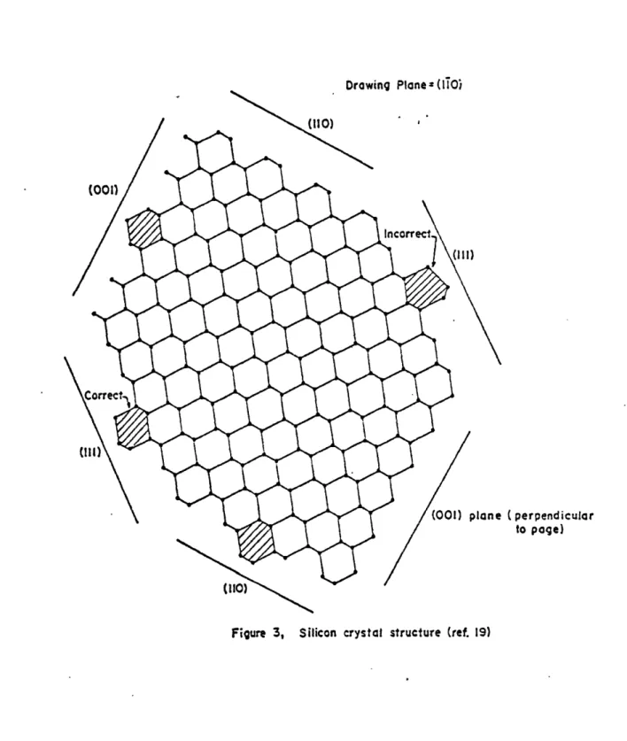
1. Models
The amorphous/cystalline interface is propagated by breaking bonds in a-Si, thereby allowing silicon atoms to be transferred across the interface to regular lattice-site positions. For growth to occur reliably, this transfer should be to positions where bonding can be established with two atoms which are already in nearest-neighbor
19
positions in the crystalline lattice. This condition is easily met
in
the <100> direction, as shown in Figure 3 by an.examination of the
t
bond angles and distances required for bonding to crystalline silicon
in various
growth
directions.
However,
in the <111>
direction,
*
silicon has a diamond cubic structure.
t silicon has tetrahedral coordination.
WM1hi MiUi -lm UIII IEII lIEYIlm iihiliI i,
20
Drawing Plane (ITO)
Incorrect
(001) plane (perpendicular
/ to page)
Figure 3, Silicon crystal structure (ref. 19)
alternate planes have atoms with only one bond accessible to atoms
19
crossing the interface, which inhibits the growth process. Drosd speculates that growth along the <111> direction involves nucleationof atomic ledges leading to irregular surfaces and twin formation. Growth in the <111> direction can lead to the formation of a high
volume density of twins, reportedly 30-40% at temperatures between 450
20
and 5750C. The anisotropic character of the growth process results in growth rates which vary by as much as two orders of magnitude for
20
different directions. Growth is fastest in the <100> direction, and slowest in the <111> direction. If the crystallite boundary structure and growth directions are variable, say, due to twin formation during crystallization, anisotropic growth of crystallites
23
could result.2. Rates and activation eneries. oure a-Si.
The kinetics of the regrowth of amorphous silicon created by ion-implantation of single crystal silicon have been investigated by
20
19
Caepregi and Drosd, but by different methodologies. Whereas Drosd measured growth rates in annealed thin films by TEM, Csepregi used Rutherford (neutron) backscattering to monitor growth rates. As shown in Figure 4, regrowth rates for nearly 'all orientations and temperatures were higher in Drosd's study than in Csepregi's, by as much as an order of magnitude at 7000C. Furthermore, the activation
energies measured also differ significantly. Drosd reported an
activation energy
of 280
kJ/mole
(2.9
eV)
for regrowth in the
<100>/(010), <110>/(110), <110>/(001), and <111>/(110) orientationsGrowth rate vs temperature for a-Si
created by ion-implantation and by
vapor deposition (11)/ (110) \(100)/ (001) 110) /(001)---- DROSO 0001 \ \ " ret 19 "- KOSTER\ rot t4 \X 2 10 Co 10 w I-to 10 I I I . t L I i _
Figure 4: Growth rates
1.2 1.3 1.4
1 o3/T t(K )i
versus temperature, pure a-Si .. ( 10)/(110) DROSO ref. 19
\s
-1 10 -2 10 II II l ^ Ylll lldlnld nnll III II kh,rlmtdl<100> directions where the plane of the silicon substrate from which
20
regrowth initiates is a (010) plane. Csepregi et al., however, cite a somewhat lower activation energy, 232 kJ/mole (2.4 eV) for regrowth in
the <100>, <110> and <511> orientations (475-5750 C).
Two studies of growth during the crystallization of evaporated amorphous silicon, deposited at T =25 C have been performed. Zellama
15
et al. investigated growth rates by measuring changes in electrical 14
conductivity during crystallization. Koster investigated growth using hot-stage TEM, in which the a-Si foil is annealed in the microscope.
The activation energy for growth was reported to be 232 kJ/mole
(2.4 eV) by Zellama (560-6000C) and 280 kJ/mole (2.9 eV) by Koster
(550- 70T0 C). Direct comparision of growth rates is not possible since Zellama did not report this rate for his evaporated a-Si films deposited at T =250C. Zellama did report growth rates for evaporated a-Si deposited at T
=300
0C. However, the activation energy for growth of the T=3000C
film (473 kJ/mole) is much higher than for these otherS
(Ts=250 C) films.
3. Imouritv effects
Impurities in amorphous silicon can either increase or decrease the growth rate during crystallization, as shown in Figure 5.
Impurities seem to affect both the activation energy and the driving force (the pre-exponential) for growth, as can be shown using
850
750
650
600 550
500
450
0C
I I I I I I I
Growth rates in the recrystallization of
amorphous silicon created by
ion-implantation:
impurity effects
on growth in
the
(100) direction
31
16
-2
P
,IOcm
\k ref.
22
16
16 -2
0, 1.4XIO cm
ref. 21\
12
15
C,4.3XIO
ref.
21
14
I5
N,6.4X
10
ref.
21
15
2.9X 10
ref.
21
11
16 -2
8, 1.4 X10 cm
\
ref.
22
\
-2
cm
cm-2
-2
cm
\
no doping
15 -2
8.2X
10
cm
ref.
21
0.8
Figure 5: Growth0.9
1.0
1.1
1.2
1.3
10
3/T
(OK
)
4rates versus temperature, impurityv effects
4
10
3
10
2
10
4-CE
4- 4=-o 0 . (310
40
Ar,
I-Y IIYIY _ ul~
--4. Effect of a-Si density on j-= th
The density of amorphcus silicon can significantly affect the growth rate. Slight decreases in the density of amorphous silicon
20
from the crystalline value tend to increase the growth rate. Large
decreases in the density (8%) from the crystalline value can reduce 24
the growth rate by an order of magnitude.
5. General exoression
In general, the rate of growth during transformation may be described using the expression :
V = (kT/h) (A"/RT)exp-(AF ) G/RT] (3) A G
where (AF )G is the free energy of activation for
transformation boundary migration. AF is the free energy difference
per mole for phases on the two
sides of the boundary 6 is the boundary thickness
13 -1
kT/hceI0 s ar 700 C
25
In Turnbull's development, the AF/RT pre-exponential term is
associated with the driving force for boundary migration bu= -AF
where N is Avagadros number. At higher driving forces, this relation
is expressed more precisely as
V,= (kT/h)expf-( F )G/RT] [I-exp(&F/RT)
g G
which has been applied to growth in the crystallization of a-Si by 15
Zellama et al.
* characteristic of evaporated a-Si films.
t used by Turnbull (Ref. 25) to describe the rate of grain growth in the recrystallization of metals.
IV. Description of Work
A transmission electron microscope (TEM) study of the kinetics of
crystallization of amorphous silicon was conducted. The nucleation and growth rates, and their time dependencies were determined. Efforts were made to correlate them to the chemistry and microstructure of the as-deposited films.
The two films principly investigated were deposited by rf-sputtering and chemical vapor deposition (CVD), and were amorphous
as determined by electron diffraction. The deposition conditions are
specified in Table 1. The CVD film was deposited at Lincoln Labs (M.I.T.) through the efforts of M. Geiss (Lincoln Lab) and Prof. H.
Smith (M.I.T.).
These samples were
isothermally annealed for various
lengths of
time (Table 2) and the resulting films examined by TEM.' The annealing
temperatures were approximately the crystallization temperatures determined by X-ray diffraction (Appendix 1), for a 16 hour anneal.
In a more extensive project the activation energies for nucleation and growth would have been determined. However, a considerable amount of supplimentary data is required to properly interpret these activation energies. Since neither the activation energies or this other data was nessesary to immediate project concerns, measurement of
Table 1: Deposition parameters
Rf-sputtered (0S!-023): Polycrystalline Si target
-6
Ultimate Vacuum: 3x10 Torr
Argon Plasma Pressure: 8.5 mTorr Accelerating Potential: 1210 7 Substrate Temperature: 4000C Film Thickness: 1.2 gm
Deposition Rate: 13.3 rn/min
CVD (Chemical Vapor Deposition):
90cc/min 5% SiH in Argon
90cc/min N
Total Pressure: 760 Torr (1 atm) Reactor Temperature: 610 0C
Film Thickness: 1 tm
Deposition Rate: 20rnm/min
Table 2: Annealing times and temperatures
Rr-sputtered (OS1-023): 7240C for 3.5, 5, 7, 9, and 15 hours
CVD : 5510C for 3, 5, 7, 16, and 23 hours 8120C for 16 hours
A. Experimental Apparatus and Procedure
The experimental procedure was to; obtain a substrate, clean it, deposit amorphous silicon on it, cut or scribe and break it into 1 cm by 1 cm squares, clean if nessesary, perform isothermal anneals of the samples, and prepare TEM specimens. These operations are discussed in terms of their fundamental components; substrates, cleaning procedure, annealing procedure, and TEM-specimen preparation and interpretation.
1. Substrate
Several criterion were developed for selecting an appropriate substrate for this study. An optimum substrate must be:
1) non-crystalline
2) chemically inert and resistant to diffusion
3) macroscopically, and preferably, microscopically smooth.
4) thermally matched to silicon, i.e. it should have thermal expansion coefficients close to that of silicon.
5) resistant to spalling, or delamination of the silicon film.
Several possible substrate materials which met at least some of these criteria were tested.
Vitreous carbon substrates were amorphous, had desirable thermal expansion characteristics and were electrically conductive, which would have been desirable for device applications. However, the adhesion of the amorphous silicon was poor, and delamination of small flakes of of silicon occured within a couple of days at room ambient.
J to prevent heteroepitaxy or localized strain effects at kinks and
cleavage planes on the substrate (Ref. 26).
Fused silica substrates* satisfied the first three criteria. However, a combination of stresses from the crystallization process and from the mismatch of thermal expansion coefficients caused microcracks to propagate through both the deposited layer and into the
substrate during anneal.
Various metals and oxide ceramics (e.g.
alumina) .were
considered
and rejected as possible substrate materials due to inadequacies inone or more of the criteria above.
Therefore oxidized sngle crystal silicon substrates were employed in this study because they satisfied all of the criteria and were cost effective for research purposes. The oxide layer was
550 nm thick, created by a thermal oxidation process and was amorphous
as determined by electron diffraction and dark-field TEM. 2. Cleanin Procedure
The cleaning procedure used for this study consists of degreasing the substrate by successive application of hot trichloroethylene, acetone, methanol and deionized water, as described in Table 3. It
has been employed successfully elsewhere for silicon microelectronics research.2 8
* Accumet Engineering Corp, Hudson MA
** also reported by Janai et al (Ref. 27) t Mosfet Micro Labs, Inc., Quakertown PA
Table 3: Substrate cleaning procedure
1) Boil wafer(s) in trichloroethylene for 5 minutes.
2) Ultrasonic clean wafer(s) in hot trichloroethylene for 5 minutes.
3) Heat wafer(s) in acetone to the boiling point.
4) Ultrasonic clean in hot acetone for 5 minutes. Decant. 5) Boil wafer(s) in methanol for 10 minutes. Decant.
6) Ultrasonic clean wafer(s) in\ distilled, deionized water for 10 minutes.
7) Place wafer(s) on edge, allowing water to run off. A nitrogen gun may be used to assist this process.
i II 1 IlbhmIl
3.
Decosition Processes
a. rf-souttered films
A rf (radio frequency) field is applied between two electrodes to
+
accelerate Ar ions toward the silicon target. Silicon is removed and 29
redeposited on the substrate.
A Materials Research Corporation model 8620 rf-sputtering unit was
used to deposit the 0S1-023
a-Si films used in
this study.
The
substrate-target distance
was 5.5 cm.
Tne substrates were heated to
4000C during deposition with an electric heater in the substrateholder (one of the electrodes). A thermally conducting paste insured
good thermal contact between the substrate and this heater. The
deposition parameters for the rf-sputtered films used in this study are listed in Table 1.
b. Chemical Va2or Deoosition
CVD films used in this study were deposited in a low-pressure thermal reactor at Lincoln Labs (M.I.T.), courtesy of Prof. H. Smith
and M. Geiss.
The CVD process involves the thermal decomposition of silane gas in the presence of a substrate. Deposition parameters for the CVD films used in this study are listed in Table 1. The reactor used a flowing gas system with argon and nitrogen as carrier gases.
4. Annealing furnace and orocedure
A conventional tube furnace was used in all annealing experiments. The sample sat in a high purity alumina boat, in a Vycor (TM) tube which extended through the furnace core. High purity (99.995', <10 ppm H20, <10 ppm 02) He flowed through the Vycor tube,exiting through
an oil bubbler. An on-off controller regulated temperature via a thermocouple in the furnace. A second thermocouple located next to the sample permitted accurate monitoring of its temperature. The furnace could be brought to temperature without heating the sample by
sliding the Vycor tube and sample boat until the later was well outside the furnace core. ThiA was done to minimize the heating times for the sample. The samples remained in the Vycor tube with He flowing until cooled to room temperature at the end of anneal.
5. Transmission Electron Mcroscoov
Transmission electron microscopy (TEM) involves two related concerns: specimen preparation and image interpretation. Both have inherent difficulties.
a. Soecimen oreoaration
TEM sample preparation consisted of mechanical thinning of the substrate, chemical etching of the substrate (84 ml HNO3, 28 ml HF,
55 ml acetic acid, 0. 1258 iodine), and ion-milling to perforation of
the deposited layer. The exact procedure used is detailed in
Appendix 2. Ion milling was performed at 3-4.5 kV ion accelerating potential and 10-15 degree angle relative to the plane of the plane of the sample. The accelerating potential used increased with the
crystallinity of the depoaited silicon film,.
b. Artifacts
One of
the primary difficulties associated with
this study was
artifacts introduced by the sample preparation technique.The etching solution used in this study (Appendix 2) had been 19
ion-implantation. However, this etchant left well defined etch pits
5 nm in diameter on the rf-sputtered films. Acid solutions consisting
of nitric and hydrofloric acids, and water or acetic acid were found
to have slow and non-reproducible etching characteristics if used on
small areas or silicon. This was probably associated with the high
stability and adhesion of gas bubbles evolved during etching to the
sample surface. Another difficulty inherent to chemical etching of
a-Si is that the density and chemical reactivity of amorphous silicon
changes with the specifics of deposition and heat treatment resulting
in highly variable etching behavior. Therefore ion-milling was
employed in the final thinning of the samples.
On the basis of an investigation of variables in the ion-milling
+
process, silicon films were milled at 3 kV Ar accelerating potential
for a-Si and at 4-5 kV for polycrystalline silicon. c. TnterDretation of TZM results
The effective resolution limit of TEM for detecting second phases
30
in amorphous silicon is about 5 n in 100-200 n thick films. This
effective resolution limit arises from the nature of inelastic
electron scattering processes in a-Si, which result in a non-uniform
contrast feature for a-Si in the TEM image. Due to the short range
31
order in a-Si (crystalline coordination to the nearest neighbors),
electron scattering processes create regions of electron phase
32-34
coherency some 1-5 rnm in diameter. These appear as alternating light
have no unique structural interpretation. Transmission electron microscopy was conducted on a Phillips EM300 microscope.
Other complications arose in interpreting the TEM images of
specific samples.
In the 0S1-023
(T =400
C) rf-sputtered films,
crystallite
boundaries could not be reliably resolved from other features inbright-field TEM. Therefqre, dark-field TEM was employed in analysing these specimens. In the dark-field technique some, but not all diffracting grains are imaged. These imaged grains will appear bright in the dark-field image. Their intensity will depend on how strongly they diffract (i.e. their orientation relative to the beam), and scattering of electrons as they pass through other grains in the
"thin" foil.
The inability to obtain data
from
bright-field TEM,
for the
rf-sputtered film, created several difficulties. One of these was possible distortion of the crystallite size distribution by overlaps of diffracting grains resulting in larger apparent crystallite sizes than were the case. The high density of twins in these crystallites, and the associated changes in contrast within the grain made it difficult to judge whether the larger features in dark-field were one crystallite with twins or several overlapping crystallites. Since grain sizes were typically 10 rm in a film 150-200 r thick, there was a significant probability of multiple grains partially overlapping.* the line resolution (for crystalline samples) of the microscope
-- --- -- --- IIYOI~ 1Yl YIhIEEIIIIIEYIHII
35
In some cases this could be observed by tilting the beam during
dark-field TEM work.
Tne dominant difficulty was in developing a correlation between
the density of features in dark-field TEM and the actual crystallite
density in the film in the absense of reliable bright-field data.
This correlation factor depends principly on the statistics of
diffraction processes for the grains in the field of view of the
microscope and is estimated in Appendix 3 for the (0S1-023)
V. Results and Discussion
The structure and chemistry, and resulting nucleation and growth
behavior during crystallization seem to be specific to the method and
parameters of deposition of the amorphous
silicon.
The
nucleation
rates for
rf-sputter (OS1-023) and CVD deposited amorphous silicon
films are substantially higher than reported for some evaporated a-Si
films.
Growth
of
crystallites in
the rf-sputtered film (OS1-023)
seems to be slowed or arrested through a
combination of pinning
mechanisms including
impurity and pore drag.
The growth rate in the
CVD film was
somewhat
lower than reported for evaporated a-Si and is
anisotropic in character.
A. As-deposited silicon films
The as-deposited
(0SI-023)
rf-sputtered
films
exhibited coalescense
islands which were polyhedral in shape with an average size
of 37.1 as
and a standard deviation
of
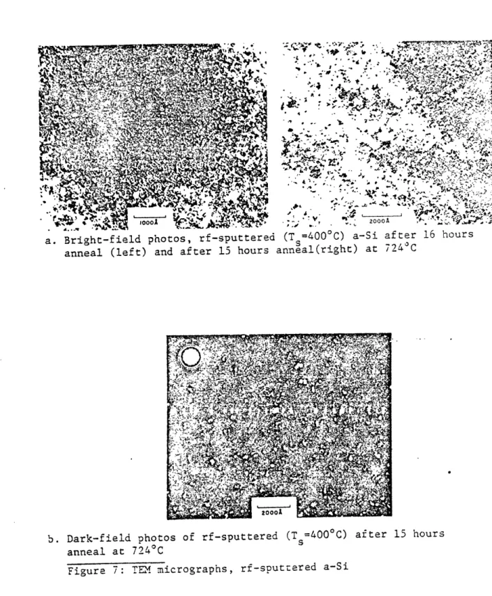
16.5 rn, (see Micrographs,
Figures
6-7).
35
Knights et al. have reported a similiar structure, with coalescense
islands 16 anm in diameter in plasma-deposited hydrogenated amorphous silicon (a-Si:H). The relative sizes of these islands may be associated with the difference in substrate temperatures duringdeposition, Ts
=230
OC in Knights study and T =4000C in our work. 35Knights et al performed extensive characterization of their a-Si:H film and concluded that the region between coalescense islands is a low density a-Si structure, not an interconnected pore structure. This, and the high mechanical stability of the very thin sections of the rtf-sputtered films used in TEM suggest that the regions between coalescense islands in our films are also a low-density a-Si structure.
-~j o I.J* *0 0' ft (D) '0 ft ft (0 C) rt H (D 09 Ct U' H4 0ot U1) rtr -4 Q '-'3 ::r~ 0-. 0 ft frt p-s. Po 0 ft D m
I V
:jTo2w
*000oA
. . : ,0 o
". '~~g
-' " '
,?,; c; :
.? rdL~C
..¢""
zoo0,
:-.
;-a. Bright-field photos, rf-sputtered (T =400'C) a-Si after 16 hours anneal (left) and after 15 hours anneal(right) at 724'C
b. Dark-field photos of rf-sputtered (Ts=4000C) after 15 hours anneal at 7240C
Figure 7: T4M micrographs, rf-sputtered a-Si
II_-39
In contrast, the CVD deposited silicon film of this study
exhibited no distinct structure.
Electron diffraction and dark-field TEM results indicated that
both of these as-deposited films were amorphous. B. Determination of crvstallinitv
Although electron diffraction may be one of the best methods of
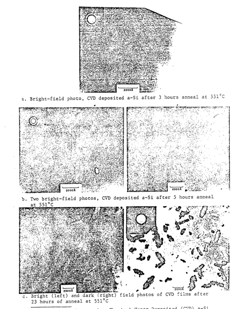
determining the crystallinity of the samples, it seems that the silicon film can have significant crystallinity before it becomes apparent by this technique. Electron diffraction patterns for CVD deposited silicon indicate an amorphous structure despite the obvious presence of crystallites in both bright and dark-field TEM for CVD
films annealed at 551C for 5 hours, (see Micrographs, Figures 8-9).
A similiar difficulty is apparent with X-ray diffraction. X-ray
diffraction indicated that (OS1-023) rf-sputtered silicon is amorphous
unless annealed at 724 OC or higher temperatures for 16 hours. However, dark-field TEM indicates the presence of some crystallites in
this film after only 3.5 hours of anneal at 7240 C.
The sensitivity ol" either of these diffraction techniques to the presence of crystallinity depends significantly on the size and
distribution of these crystallites. One reason is that the nearest
neighbor coordination in a-Si is identical to that in the crystalline
31
phase. The second and third nearest-neighbor distances are slighly distorted and have a great deal of dispersion relative to the
31,37
crystalline pnase. Additionally, small crystallites would not
necessarily have a distinctive diffraction pattern relative to a-Si
-- I ----_~ Ei-iirT_-Y---~----UI - -*rrC-X c~-f~ - L
a. Bright-field photo, CVD deposited a-Si after 3 hours anneal at 551SC
11 111, Qw Ir
41
11 III, I MCI~r 1 r~ ~
r rrts~-~n'.'~r r "ry t~
V774 N ' 1
KYt Jr -n'
S r" ;i
~'
r 200011 V 20001
ul w
b. Two brigt-fedpooV eoiedaS
at001 _________ 2000
b. To bigh-fild hoto, CD dposteda-Siaftr 5hous anea
at D-510C' ;~j r;?~
~2000120001
c. Bright (left) and dark (right) field photos of CVD films after 23 hours of anneal at 5510C
Figure 8: TEM micrographs, Chemical Vapor Deposited (CD) a-Si
i
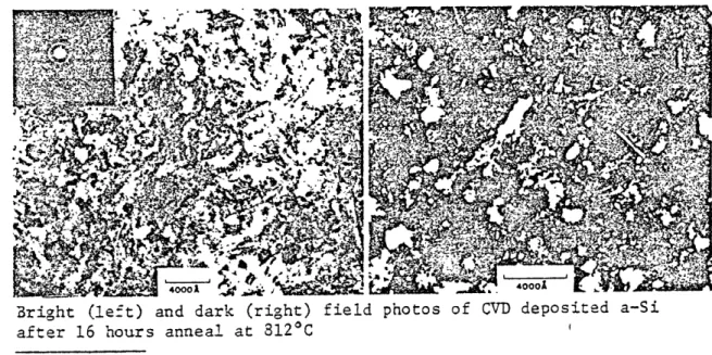
4r ON 40001 4 00011C
Bright (left) and dark (right) field photos of CVD deposited a-Si
after 16 hours anneal at 8120C
due to particle size broadening. Thus, electron diffraction seems to have limited usefulness in detecting small crystallites in a-Si.
Bright-field TEM is considerably more sensitive to the presence of
second phases than electron diffraction, but can not be used to
uniquely determine whether the second phase is crystalline silicon. Dark-field TEM seems to have a greater sensitivity to the presence of crystallites than electron diffraction or bright-field TEM. The disadvantage of dark-field TEM is that its sensitivity is dependent on
the size and distribution of the crystallites. It is statistically
reliable only when a large number of orystallites are present in the field of view of the microscope for only those grains diffracting in specific orientations are imaged in dark-field TEM.
C. £f-sDuttred
ilms
1. Nucleation rates
The nucleation rates for our rf-sputtered films were calculated from dark-field data, using the correlation factor calculated in Appendix 3 whion was estimated to be a factor of 98 crystallites in the field of
view for each one evident in the dark-field TEM images. The number
density of features in the dark-field image (see Micrographs,
Figures 6-7) was determined assuming a film thickness of 200 rn. The number density was adjusted by the correlation factor and divided by the anneal time to yield an effective nucleation rate.
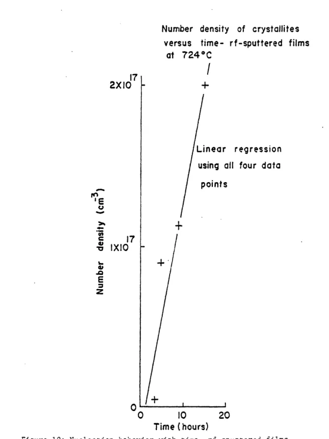
The steady state nucleation rate for the (OS1-023) rf-sputtered
12
3
silicon film is 4.1x1C /cm s at 724"C, as determined by linear
regression of our nucleation data, (Figure 10). This steady state nucleation rate is four orders of magnitude higher than reported by
17
2XIO
E
4,.
17
E
z
Number density of crystallites
versus time- rf-sputtered films
at
724*C
/
+
Linear regression
using oil four data
points
+
-I-+
10
10
20
Time (hours)
Figure 10: Nucleation behavior with time, rf-sputtered films at 7240C
14
Koster, at 7240C. However, it is only two orders of magnitude
15
higher than
the
rate at 724 OC extrapolated
from
Zellama's data.
Both of these were for evaporated a-Si films.
11 3 The average nucleation rate over the 3.5 hr anneal is 3.3x10 /cm s
(see Table I), which is an order of magnitude lower than the steady
state rate determined by ;inear regression of our nucleation data (Figure 10). If the difference in these two nucleation rates is associated with a transient effect, a 1.9 hour transient time is
calculated using a two term expansion of Equation (2). Koster has reported a transient in nucleation of 41 minutes at 650*C for
evaporated
(Ts=25C) a-Si which was
calculated
using Equation
(2).
The transient in nucleation
for
Koster's film should be even
smaller
14,16
at 724
0C.
2. Growth in Xt-suttered filmA
Rigorous analysis of
the crystallite
size
distributions
to
determine
the growth rates during the crystallization of rf-sputtered
a-Si is
non-trivial.
The means of
the apparent
crystallite size
distributions depend on both
the nucleation and growth rates.
The
maximum observed sizes give a better indication of the
growth
rates,
but have questionable statistical validity.
Examination of the
crystallite
size distributions
for
the
rf-sputtered films (Figures 11-12) suggests that no statisticalreliablity is gained by using crystallite
sizes
between the average
and maximum sizes in these distributions in growth rate determination
since the distributions are not continuous.
Finally, the crystallites
Table 4: Nucleation rates, rf-sputtered (OS1-023) a-Si at 7240 C
Anneal Average Nucleation
Time rate over the
anneal period 11 3
3.5 hr
3.3x10
/cm s
-5 5.0C10129
3.5%1012
15 hr
3.7x10 1/cm 3sOSI-023 3.5 hr, mojor a. 150 300 450 600 750 05s1023 Shr, line 150 300 450 600 750 900A OSI-023 7.5 hr, 1;1a ,, n sno 7s50 900
Figure 11: Crystallite size distributions, rf-sputtered films at 7240 C
Major-length of major axis measured. This was done on the 3.5 hour sample for the crystallite density in the
micrographs was not high enough for reliable line analysis.
Line-length of a random line segment subtending a crystallite measured. 9 00oo b. c cr c ¢. C. -- --~--LI-~ -- ____ -7 --rrv --1V Jv
OSI-023 9hr, line
a.
150 300 450 600k OSI-023 4I. 9hr, mojor OSO-023 - 15hr, line b. ISO 300 450 sooAFigure 12: Crystallite size distributions, rf-sputtered films at 7240C Major-length of major axis was measured
Line- length of a random line segment subtending a crystallite
measured. Both major and line analysis performed on the
9 hour sample for comparision, although sample size is
in the rf-sputtered film seem to exhibit anisotropic growth, but associated distortions of the size distributions are relatively small. However, some conclusions about the approximate growth rate and time
dependencies are possible.
The initial growth rate calculated using the maximum observed -3
crystallite size is 6.4x10 -3nm/sec at 724'C for the rf-sputtered film.
This growth rate decreases to zero during anneals longer than 3.5
hours at 7240 C. The initial growth rate calculated using the mean
crystallite size is a factor of 4.6 lower than that calculated using
the maximum observed crystallite size. .These growth rates are considerably smaller than the growth rates reported for evaporated
14 15
a-Si at 7240 C by Koster, 4.5 nm/sec, or by Zellama, 10 nm/sec.
The growth rate, as measured using the mean crystallite size, slows down over a 5 hour anneal, approaching zero during anneals longer than 7.5 hours, as shown in Figure 13. Furthermore, the maximum observed crystallite size remains approximately constant over anneals longer than 3.5 hours at 724 OC. There are, however, some shifts in the size distribution for it becomes less symetrical with
time. The nucleation rate is relatively constant (over anneal times longer than 3>5 hours), suggesting that the growth rate may decrease with increasing volume fraction transformed. The impingement of
crystallites should not have significantly affected growth rates for this film becomes crystalline by X-ray diffraction only after 16 hours of anneal at 724 C. Integration of the steady state nucleation rate over time, combined with an estimate of the volume occupied by each crystallite (assumed size=10 am) yields a calculated volume percent
I I 0
o
200
0 +5
10
15
time
(hr)
Figure
13'
mean sizes vs time rf
-sputtered
(OSI-023) film annealed at 724
*C
o major axis
*
minor axis
+ line
-
average
length of a line segment
Line analysis could not be used reliably on micrographs for the
3.5 hour anneal. Both line(length of a line subtending a crystallite) and point (measurement of major and minor axes) analysis was perf'ormed on the 9 hour sample to determine their relationship.
S50
crystallized of
11%
after
7.5
hours
of
anneal
at 724*C,
which
increases
to 23%
after
16 hours anneal
at 724 OC.
Thus,
crystallite
growth
is
slowed
or
arrested in
the initial
stages of
the
transformation
process.
The
crystallite size
distributions are highly
skewed so
that the maxima of these distributions
(about
10
nm)
are
probably more representative of the
crystallite
size than
the average
sizes in these distributions (about 15 am).
Two
processes may explain the anomalously slow or arrested growth
kinetics, pinning
of
crystallite
boundaries
by either
argon impurities
or
by
pore
drag as
crystallites impinge
on the edges
of
coalescense
islands
in the rf-sputtered film.
a. Pinning by argon
Data by other investigators on the regrowth of
amorphous
silicon
created
by the
implantation
of
argon
into crystalline silicon
indicates that argon concentrations in excess of 0.3 at% reduce the
regrowth rate about three orders
of magnitude (Figure 5), to near zero
28
at 650*C.
X-ray flourescense performed by
I.
Kohatsu indicates
that the
(0S1-023) rf-sputtered films may centain up to 3.6 at% argon. This
estimate is consistent with reports in the literature
of 1 to 5 at%
20,39
argon in rf-sputtered a-Si films.Our SIMS results indicate that only acout 30% of the argon annneals out of the film at 749 OC, over 16 hours. This seems to be
38
comparable to results obtained by Revesz et al. inwhich 30-40% of the
, formerly with this project
argon (0.5 at% levels) was annealed out or a-Si created by argon and silicon ion-implantation, in 8.3 hours at 6300C. The film thicknesses were 1200 nm and 100 rn, respectively.
Argon is
insoluble* in crystalline
silicon.
Hence,
as
the
transformation proceeds,
higher
concentrations
of
argon will
be
present at crystallite boundaries due to rejection of argon
from
the
crystalline
pnase.
As
the transformation progresses, this impurity
drag effect should beccme more severe as relatively little of
the
argon seems to be annealed out of the film.
No evidence was found to indicate the formation of argon
bubbles
in the rf-sputtered film.
The crystallites were typically less than
38 nm in size, hence the formation of argon bubbles
small
enough
to
40
breakaway from the a/c interface,
into the crystalline phase would
41
have been a relatively high energy
process.
Therefore,
it
seems
unlikely
that the formation of argon
bubbles was significant in
reducing the chemical impurity pinning at these boundaries.b. Pinning at internal boundaries
The boundaries between coalescense islands may also have a significant effect on growth kinetics. Generally, the crystallite sizes were smaller than the average size of these coalescense islands,
37 nm. In all cases in the (OS1-023) rf-sputtered silicon films, the maximum grain size is no larger than about twice the mean coalescense island size (as-deposited), or within two standard deviations of this
mean size. The size of the crystallites, therefore, may be limited by the width of these coalescense islands. We were unable to determine