Publisher’s version / Version de l'éditeur:
ECS Transactions, 85, 3, pp. 41-52, 2018-04-05
READ THESE TERMS AND CONDITIONS CAREFULLY BEFORE USING THIS WEBSITE.
https://nrc-publications.canada.ca/eng/copyright
Vous avez des questions? Nous pouvons vous aider. Pour communiquer directement avec un auteur, consultez la première page de la revue dans laquelle son article a été publié afin de trouver ses coordonnées. Si vous n’arrivez pas à les repérer, communiquez avec nous à [email protected].
Questions? Contact the NRC Publications Archive team at
[email protected]. If you wish to email the authors directly, please see the first page of the publication for their contact information.
Archives des publications du CNRC
This publication could be one of several versions: author’s original, accepted manuscript or the publisher’s version. / La version de cette publication peut être l’une des suivantes : la version prépublication de l’auteur, la version acceptée du manuscrit ou la version de l’éditeur.
For the publisher’s version, please access the DOI link below./ Pour consulter la version de l’éditeur, utilisez le lien DOI ci-dessous.
https://doi.org/10.1149/08503.0041ecst
Access and use of this website and the material on it are subject to the Terms and Conditions set forth at
Emission from strained germanium nanocrystals
Rowell, Nelson L.; Lockwood, David J.
https://publications-cnrc.canada.ca/fra/droits
L’accès à ce site Web et l’utilisation de son contenu sont assujettis aux conditions présentées dans le site LISEZ CES CONDITIONS ATTENTIVEMENT AVANT D’UTILISER CE SITE WEB.
NRC Publications Record / Notice d'Archives des publications de CNRC:
https://nrc-publications.canada.ca/eng/view/object/?id=26e97e53-87e0-4a76-8dab-cfbb84c25b64 https://publications-cnrc.canada.ca/fra/voir/objet/?id=26e97e53-87e0-4a76-8dab-cfbb84c25b64
Emission from Strained Germanium Nanocrystals
N.L. Rowell and D.J. Lockwood
National Research Council, Ottawa, Ontario K1A 0R6, Canada We analyse the intense photoluminescence (PL) observed at energies from 600 to 1500 meV for many molecular beam epitaxy grown Si1-xGex epitaxial layers. We show that the unexplained
broad PL peak is due to self-assembled Ge nanocrystals (NCs) within the SiGe layers. The NCs are assumed lattice matched to the SiGe in the vertical, growth direction. As the Ge-fraction in the SiGe layer increases, the vertical strain in the NCs changes from compressive to tensile at x ~ 0.36, lowering the NC band gap (BG) below that of bulk Ge. We analyse PL results for 64 samples exhibiting this broad PL peak by examining how it follows the strained Ge BG for x from 0.05 to 0.53. The PL is resolvable as two narrower peaks separated by the TO phonon energy for Ge. Strain and confinement shifted NC bound exciton energies calculated numerically agree well with the measured ones.
Introduction
A silicon-compatible group IV coherent light source remains the missing link in Si-based photonics, despite the great variety of approaches explored; e.g., carrier localization, rare-earth doping, and stimulated light scattering. Although achieving efficient light emission from group IV semiconducting materials, a subject of intense research activity, has proven elusive, carrier localization methods have led to significantly enhanced optical emission from indirect gap materials and, notably, at higher temperatures. For example, room-temperature visible photoluminescence (PL) has been observed from porous Si (1) and strong infrared PL from various island or quantum dot systems (2-9). A particular focus has been the study of self-organized structures containing nanometer sized Si (10) and Ge crystals (11), which being compatible with present Si technology have important capabilities for device engineering. Applications include those in optoelectronics (12), tunneling devices (13-15), and nanocrystal memories (10,16). Recently, lasing or very high efficiency photoluminescence (PL) has been shown for germanium (Ge), a material with a relatively small indirect to direct bandgap (BG) difference, which can be overcome with tensile strain and/or high doping (17-20), or by alloying with tin (21).
Previously (22) we observed a very intense, low temperature PL with a large lifetime in dozens of our samples for molecular beam epitaxy (MBE)-grown Si1-xGex epitaxial
layers with x ranging from 0.05 to 0.53. Efficiencies in the 5% range – unheard of for group IV materials – were observed. This PL was neither defect nor dislocation related, and was suspected to be due to carrier localization effects.
Experiment
Although the present work is largely an interpretation of prior results, a brief description will be given as to how the samples in question were grown and their properties measured (22).
Growth was by conventional, solid source MBE without intentional doping in an ultrahigh vacuum deposition chamber. The growth temperature was measured with an optical pyrometer in the range 350 - 900°C. The Si growth rate was 1 Å/s and the Ge growth rate was set to achieve a given value of x. The single or multiple quantum well structures were designed to be stable with respect to misfit strain relaxation (23).
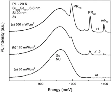
The PL spectra were measured using a Bomem DA3 FTIR spectrometer with samples generally at ~5 K excited with 1 to 300 mW of either 457.9, 488.0, or 514.5 nm laser light from an argon ion laser. Varying the wavelength of the exciting light affected the depth of penetration into the sample. The advantages of using a Fourier transform spectrometer for PL studies are well known (24). A radiometric calibration was performed to obtain the relative spectral responsivity of the system from 500 to 1400 meV, which was used to normalize the raw spectral data. The PL spectra with broad peaks for 64 separate MBE growths were examined. Of these samples 30 had both broad and phonon resolved (PR) peaks in their spectra. In Fig. 1 we see an example of a sample which exhibits both broad and PR PL. In that figure we see that at higher laser power densities the centers responsible for the broad PL become saturated and the PR peaks are more apparent. The main PR peaks are the no phonon (NP) peak associated with the SiGe BG and its transverse optic (TO) phonon replica, which are separated by 58 meV. The broad PL peak is approximately 100 meV lower in energy than the PRNP peak.
The Si1-xGex well thickness and Ge fraction were determined using x-ray
double-crystal diffraction and dynamical rocking curve analysis which yielded an absolute uncertainty in x of ± 0.02 (25). For samples exhibiting both broad and PR PL, the no phonon peak position in the PR spectrum was used as a separate indicator of layer thickness and Ge fraction (as in Fig. 1).
Figure 1. Low temperature PL spectra of a triplet quantum well sample with x = 0.17 showing at various excitation intensities both the broad and phonon resolved (PR) PL and a feature due to the Si substrate (subTO).
Results and Discussion
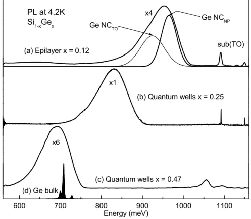
As shown in Figs. 1 and 2, the PL consisted of a broad peak with an asymmetry to low photon energies. This peak displayed little variation in shape with Ge fraction and tracked the BG variation, but was always ~100 meV below the indirect SiGe BG. The width of this peak at ~ 50 meV was too small for it to be due to a no phonon (NP) line with its TO phonon replica if the material were Si or SiGe, as the NP-TO spacing is about 58 meV for those materials. Fig. 2 shows that for higher Ge fractions the PL is emitted at energies significantly below those for bulk Ge, with its indirect BG of 744 meV at low temperatures. The origin of the broad, intense PL peak has remained unexplained, until now.
Figure 2. Low temperature PL from three SiGe samples and bulk Ge. For the spectrum in trace (a), the result is also illustrated with curve fitting using two Gaussian peaks for the broad PL peak.
Self-Assembled Ge Nanocrystals – Lattice Matching
An examination of the available experimental evidence indicates that the peak is probably due to imbedded Ge nanocrystals (NCs) within the SiGe layers (see Fig. 3). Evidence for the formation of such NCs was indicated by transmission electron microscopy (TEM) studies (22) and confirmed via Raman spectroscopy.
600 700 800 900 1000 1100
(d) Ge bulk
Energy (meV)
(c) Quantum wells x = 0.47 x6
(a) Epilayer x = 0.12 sub(TO)
x4 PL at 4.2K Si1-xGex (b) Quantum wells x = 0.25 x1 Ge NCTO Ge NCNP
Figure 3. Lattice matched Ge NCs in SiGe on Si(001).
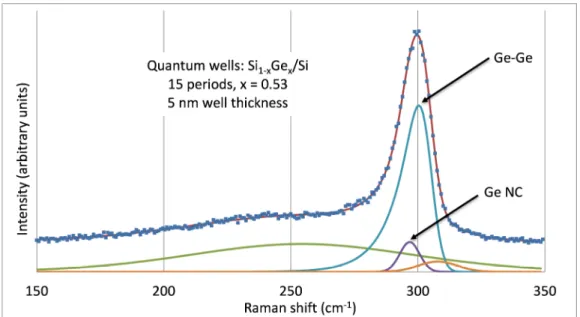
As an example, we show in Fig. 4 the Raman spectrum of a 15 period Si1-xGex/Si
multiple quantum well sample with x = 0.53 and an alloy layer thickness of 5 nm. The vertical tensile strain in an imbedded Ge NC would be 2.2% in this sample. The spectrum is readily curve-resolved into just four peaks. The strong asymmetric (Gaussian) sharp peak at 300.0 cm-1 is due to the Ge-Ge type vibrational mode associated with the strained
alloy epilayer (9), while the weaker sharp Gaussian band at 296.4 cm-1 is typical of Ge
(9). In the work of Reference 26, this amount of uniaxial strain in a Ge nanobridge gave rise to a Raman peak at 297.0 cm-1, which is quite near the value obtained here for the Ge
NCs. The very broad band at 254 cm-1 is needed to account for a continuum of
second-order Raman scattering from phonons in the epilayer, while the very weak peak at 307 cm-1 is needed to account for the tail of the Raman spectrum at higher frequency. The existence of the weak band at 296.4 cm-1 confirms the presence of Ge NCs in the SiGe
epilayer and indicates that they are under tensile strain, as its frequency lies below that of bulk (unstrained) Ge (~300 cm-1).
Figure 4. Room temperature Raman spectrum of a 15 period Si1-xGex/Si multiple
quantum well sample with x = 0.53 and well thickness of 5 nm in the frequency region of Ge-type lattice vibrations (solid points). The spectrum has been curve resolved into the components shown underneath the fitted curve (solid line).
Ge Compressive (xy)
Si
Si1-xGex Tensile (z): Ge > 0.36
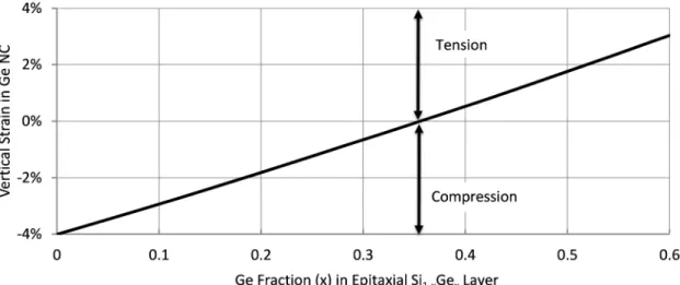
Epitaxial growth requires that the SiGe epilayers and the Ge NCs be lattice matched to Si (001) in the x-y plane, so that both the SiGe and NCs are under compression in that plane. However, the growth is unconstrained in the vertical (z) direction. Thus the epilayer is under tensile strain in this direction, leading to a vertical lattice constant that increases with Ge fraction and is larger than that for unstrained SiGe. Here the volume of the unit cell for the epitaxial SiGe layer is assumed to be the same as that for unstrained cubic (bulk) SiGe. The lattice of the Ge NCs is constrained to match the SiGe epilayer vertically. For relatively dilute SiGe, the Ge NCs are under compression vertically, but for increasing Ge content in the SiGe epilayer the vertical lattice constant of the strained SiGe eventually exceeds that of bulk Ge. At the point where the vertical strain in the Ge NC first becomes tensile, the Ge fraction in the SiGe is 0.36 (Fig. 5). With these constraints we can write down the equation for the strain in the z direction within the Ge NCs as:
= ( − )/ [1] where is the bulk Ge lattice constant (5.658 Å) and is the strained lattice constant in the vertical direction for tetragonally distorted SiGe material, which is lattice matched to Si in the horizontal plane. Note that the strain value is negative for compression and positive for tension. With increasing , this lattice constant varies from 5.431 to 6.141Å as given by the following formula:
= ( ) /( ) [2] where is the lattice constant for Si (5.431 Å). Here is the lattice constant for cubic (unstrained) SiGe given by:
= + + [3] where is the Ge fraction. In this quadratic equation, the symbols, and , represent constants equal to 0.2 and 0.027, respectively (27).
Bandgap Variation with Strain
The BG variation in Ge with uniaxial strain can be computed from deformation potential theory. As the strain becomes more strongly tensile both the direct and indirect gap energies decline, with the direct energy decreasing more rapidly than the indirect one. As shown in Fig. 6, the direct gap energy crosses over the indirect gap energy at a tensile uniaxial strain of 4%, resulting in a direct gap semiconductor, a highly desirable outcome. Our results with PL point the way to this transition point, but the maximum vertical tensile strain for the present Ge NCs is not much greater than 2%. Nonetheless, the fact that we see PL below the indirect BG of bulk Ge is explained by the Ge NCs being under tensile strain vertically, reducing their Ge BG.
Figure 5. NC vertical strain versus in Si1-xGex. Here, compressive strain is negative, and tension is positive.
With deformation theory, there are linear relationships between strain and the direct and indirect bandgaps, as per:
= + [4] where for strain expressed in per cent the intercept and slope in the linear equation are 880 and -79.3 for the direct bandgap and 740 and -45.5 for the indirect one at low temperatures (28). For example, for a tensile strain of 2%, the direct BG energy is 721 meV and the indirect BG is 649 meV.
Figure 6. Bandgap and PL energy versus Ge NC vertical strain. The bandgap curves are calculated versus strain using linear deformation potential theory. The data points are obtained by curve resolving the PL of 62 MBE-grown SiGe samples.
-4 -2 0 2 4 500 600 700 800 900 1000 1100 1200 E ne rg y (m eV ) Strain (%) Energy versus Ge NC Vertical Strain PL from 62 MBE Samples
Compression Tension
MBE PL Data
Ge Indirect
In Fig. 6 the points are Ge NCNP PL peak energies and the solid lines are the direct
and indirect NC BGs (Eq. 4). In Fig. 6 we note that the data points in energy are above the Ge indirect BG, which is most likely due to quantum confinement, as will be discussed. This is a difference that appears to decrease as compression decreases, although there are only a few points for the larger tensile strains. The energy uncertainties in the data points are those obtained from curve resolving the PL peaks. The strain uncertainties for these points are derived from the x-ray diffraction measurements of the composition and thickness of the SiGe layers.
Ge NC Phonon Peaks
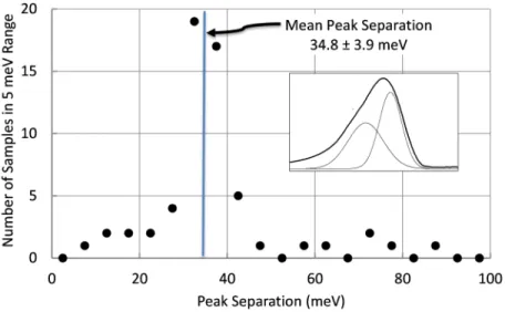
As was shown in Fig. 2(a), the broad peak’s width and asymmetric shape can be curve resolved into two symmetric peaks, separated by ~35 meV, i.e., very near the momentum conserving TO phonon energy for Ge. The NP peak is wide (25-45 meV) due to NC confinement variations arising from size variability and to alloy disorder broadening in the SiGe. In Ge dots, we expect two main PL peaks, a no phonon and TO replica line, separated by about 33 meV. So the results of curve resolving are very close to Ge TO energy for momentum conserving phonons, but far from those for Si and SiGe that would both be about 58 meV. We also notice inhomogeneous broadening due to size effects and that the NP peak is relatively large, as would occur for a high degree of carrier localization in Ge NCs.
Figure 7. Summary of the results from curve resolving two Gaussian peaks within the envelope of the broad PL peak, as illustrated in the inset. Here is shown the number of samples with peak separations within 5 meV of each other versus peak separation. For the samples studied here, the mean separation is 34.8 ± 3.9 meV, which equals the Ge TO phonon energy (33 meV), within measurement uncertainty.
Calculation of Bound Exciton Energy for Ge NCs
To test the present hypothesis further, we calculated the emission energy in a simple numerical model which accounts for the effects of strain on the Ge BG and of the confinement blue shifts in the exciton PL spectra for both the SiGe layers and the
imbedded NCs, the latter of a single size (2.5 nm high in the growth direction). In this model, the vertical direction is assumed to provide the lowest energy BG. We used a double well structure, consisting of both Ge and SiGe wells, with the smaller Ge wells completely imbedded in SiGe, as illustrated in Fig. 3. In such a system there are related confinement shifts in both the Ge NCs and the SiGe material. While the SiGe layer thicknesses were obtained from structural measurements, as discussed in the Experiment section, the NC height is not known and can be treated as somewhat of a free variable. In the formulatio, we incorporate the effect of vertical strain on the NC BG using a deformation potential approach.
Figure 8. Shooting method results for calculating the bound exciton energy in a double well Ge-SiGe/Si layered system. The left panel depicts the result for a Si0.85Ge0.15
quantum well 5 nm thick where the exciton energy obtained is approximately 1054 meV. On the right, a 2.5 nm strained Ge NC has been added. The lowest bound exciton energy in that case is 924 meV. The background energy is that of substrate bound excitons in silicon (1150 meV). The well structure shown illustrates reductions in that energy due to the presence of Ge in the SiGe alloy layer and/or in the Ge NC. The horizontal lines in the quantum wells represent the energy solutions for which the wavefunctions are well behaved well away from the quantum well in the growth direction.
To evaluate the combined effects of confinement and strain, we have used a 1-D model in the vertical (growth) direction, which we solve numerically as a double quantum well by varying the exciton energy to find its value where the wavefunction goes to zero far from the well center in both the positive and negative directions. The exciton energy is of primary importance as it is the quantity that PL measures. The object is to compare this calculated no-phonon energy, which contains the confinement and strain BG shifts as well as exciton binding energies, to the observed PL energy. The example shown in Fig. 8 is for the energies in a 5 nm thick Si0.85Ge0.15 well that contains
a 2.5 nm high Ge NC. The lowest energy of the confined excitons is in the Ge NCs at 924 meV.
Comparison of Calculated Ge NC Energy with Measured PL Peak Energy
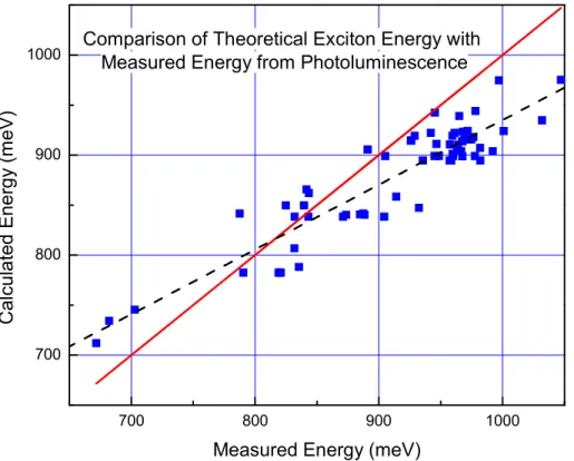
The calculated energies for 64 samples of varying composition are compared with the measured PL energies in Fig. 9. Here for simplicity we have assumed a constant NC vertical size of 2.5 nm. In Fig. 9, the best-fit straight line (shown by the dashed line) to the data is expected to have a slope near unity (as shown by the solid line in the figure) but is somewhat different from that value due to what are possibly lower order influences, such as variations in the NC size and deviations from the linear deformation potential model for the strained BG. However, we do have good general agreement between our
computed emission energies and those observed in PL, which provides reasonable validation for our theory that imbedded Ge NCs have given rise to the intense, broad PL observed in MBE grown SiGe.
Figure 9. Theory versus experiment for the Ge NC PL from SiGe samples with Ge fractions from 0.05 to 0.53. The dashed straight line is the result of a least-squares fit to the data. The solid line represents the result that one would have obtained if the measured and calculated energies were identical.
One question to answer is whether or not confinement is sufficient to account for the PL energy always being at energies above that of the strained bulk Ge BG, as shown in Fig. 6. This difference is in approximately the 50 to 150 meV range with an average of 103.4 meV. Are these values reasonable for quantum confinement effects in the Ge NCs? With the simple model described above we can calculate the size of the confinement effect versus NC size, QW thickness and composition. We generally found that the variation of NC confinement energy with thickness of the host SiGe was not that large (< 5 meV) and the variation with Ge-fraction although larger was not a major contributor to the difference. For example, the NC confinement shift for a 1.5 nm NC in a 5 nm thick well was 110 meV for a Ge-fraction of 0.15 and 130 meV for a fraction of 0.50, everything else being equal. However, NC sizes in the range from 1 to 3 nm – corresponding to confinement energies from 120 to 50 meV – can indeed account for all the blue shifts from the predicted Ge NC BG that we see in the PL energies. This means that confinement shift is an explanation for all the differences seen between the measured PL energy and the NC bandgap. But it appears from the distribution of points in Fig. 9 that the average NC size of 2.5 nm employed might have been somewhat too large. A value nearer 1.5 nm would appear to be more reasonable, begging the question as to what influences and/or limits this size. Growth conditions should of course be critical in this respect.
700 800 900 1000
700 800 900
1000 Comparison of Theoretical Exciton Energy with Measured Energy from Photoluminescence
C al cu la te d En er gy (m eV )
There are other assumptions in the simple model used here that can be questioned, not the least of which is whether or not deformation potentials describe accurately the strain effect. A tight binding model could prove to be more appropriate as discussed in Reference 28, where for high tensile strain (> 1 %) the latter model provides significantly lower indirect bandgaps in Ge than does the deformation potential approach.
Summary and Conclusions
In this work we have revisited the previously unsolved problem as to why strong PL can be observed in Si/Si1-xGex quantum well samples grown by MBE at energies not only
consistently below that of the Si1-xGex BG, but in the case of high Ge concentrations even
below that of the Ge BG. A detailed examination of the concentration dependence of the PL no-phonon energy revealed that the likely source of the strong PL was carrier confinement in Ge NCs that had grown by self-assembly in the Si1-xGex epilayers. The
presence of such NCs within the epilayers was confirmed from Raman spectroscopy measurements. A theoretical analysis based on a deformation potential model revealed that strain plays a major role in determining the Ge band gap: most significantly, the NC strain along the epilayer growth direction changes from compressive to tensile at x = 0.36, thereby explaining the previously puzzling observation of PL at energies below that of Ge. Calculations of confinement effects on the BG energy based on a double quantum well model for 2.5 nm sized Ge NCs in Si1-xGex epilayers on Si showed good qualitative
agreement with the observed PL energy variation with x. In conclusion, our modelling of the experimental results for the concentration dependence of the PL from strained Si1-xGex epilayers for 0.05 < x < 0.55 has shown that the intense PL at lower energies
arises from imbedded Ge NCs. Such structures show promise for use as light emitters in device applications if appropriate growths at high x values can be engineered to introduce the predicted transition to a direct band gap within Ge NCs for x values greater than 0.65.
Acknowledgement
The authors thank the following people for their many original contributions to the former program in SiGe epitaxy at the National Research Council of Canada: J.-P. Noël, D.C. Houghton, E. Wang, and J.-M. Baribeau.
References
1. L. T. Canham, Appl. Phys. Lett., 57, 1046 (1990).
2. J.-P. Noël, N. L. Rowell, D. C. Houghton, and D. D. Perovic, Appl. Phys. Lett.,
57, 1037 (1990).
3. N. L. Rowell, J.-P. Noël, D. C. Houghton, and M. Buchanan, Appl. Phys. Lett., 58, 957 (1991).
4. Y. S. Tang, C. M. Sotomayor Torres, W.-X. Ni, and G. V. Hansson, Superlattices
and Microstructures, 20, 505 (1996).
5. S. Fukatsu, H. Sunamura, Y. Shiraki, and S. Komiyama, Thin Solid Films, 321, 65 (1998).
6. L. Tsybeskov, K. D. Hirschman, S. P. Duttagupta, M. Zacharias, P. M. Fauchet, J. P. McCaffrey, and D. J. Lockwood, Appl. Phys. Lett., 72, 43 (1998).
7. K. Eberl, O. G. Schmidt, O. Kienzle, and F. Ernst, Thin Solid Films, 373, 164 (2000).
8. D. N. Lobanov, A. V. Novikov, N. V.Vostokov, Y. N. Drozdov, A. N. Yablonskiy, Z. F. Krasilnik, M. Stoffel, U. Denker, and O. G. Schmidt, Optical
Materials, 27, 818 (2005).
9. J.-M. Baribeau, X. Wu, N. L. Rowell, and D. J. Lockwood, J. Phys. Condens.
Matter, 18, R139 (2006).
10. A. Karmous, I. Berbezier, and A. Ronda, Phys. Rev. B, 73, 075323 (2006).
11. N.L. Rowell, D.J. Lockwood, G. Amiard, L. Favre, A. Ronda, I. Berbezier, M. Faustini, and D. Grosso, Journal of Nanoscience and Nanotechnology, 11, 9190 (2011).
12. M. H. Nayfeh, S. Rao, N. Barry, J. Therrien, G. Belomoin, A. Smith, and S. Chaieb, Appl. Phys. Lett., 80, 121 (2002).
13. L. Tsybeskov, G. F. Grom, R. Krishnan, L. Montes, P. M. Fauchet, D. Kovalev, J. Diener, V. Timoshenko, F. Koch, J. P. McCaffrey, J.-M. Baribeau, G. I. Sproule, D. J. Lockwood, Y. M. Niquet, C. Delerue and G. Allan, Europhys. Lett., 55, 552 (2001).
14. Q. Wan, T. H. Wang, M. Zhu, and C. L. Lin, Appl. Phys. Lett., 81, 538 (2002). 15. B.V. Kamenev, G. F. Grom, D. J. Lockwood, J. P. McCaffrey, B. Laikhtman and
L. Tsybeskov, Phys. Rev. B, 69, 235306 (2004).
16. Y. C. King, T.-J. King, and C. Hu, IEEE Trans. Electron Devices, 48, 696 (2001). 17. Rodolfo E. Camacho-Aguilera, Yan Cai, Neil Patel, Jonathan T. Bessette,
Marco Romagnoli, Lionel C. Kimerling, and Jurgen Michel, Kimerling, Optics
Express, 20, 11316 (2012).
18. Roman Koerner, Michael Oehme, Martin Gollhofer, Marc Schmid, Konrad Kostecki, Stefan Bechler, Daniel Widmann, Erich Kasper, and Joerg Schulze,
Optics Express, 23, 14815 (2015).
19. Jose R. Sánchez-Pérez, Cicek Boztug, Feng Chen, Faisal F. Sudradjat, Deborah M. Paskiewicz, RB Jacobson, Max G. Lagally, and Roberto Paiella, PNAS, 108, 18893–18898 (2011).
20. Jan Petykiewicz, Donguk Nam, David S. Sukhdeo, Shashank Gupta, Sonia Buckley, Alexander Y. Piggott, Jelena Vučković, and Krishna C. Saraswat, Nano Lett., 16, 2168−2173 (2016).
21. S. Wirths, R. Geiger, N. von den Driesch, G. Mussler, T. Stoica, S.Mantl, Z. Ikonic, M. Luysberg, S. Chiussi, J. M. Hartmann, H. Sigg, J. Faist, D. Buca and D. Grützmacher, Nature Photonics, 9, 88 (2015).
22. N.L. Rowell, J.-P. Noël, D.C. Houghton, A. Wang, L.C. Lenchyshyn, M.L.W. Thewalt, and D.D. Perovic, J. Appl. Phys., 74, 2790-2805, (1993).
23. D.C. Houghton, J. Appl. Phys., 70, 2136 (1991).
24. N.L. Rowell, Proceedings of International Conference on Raman and Luminescence Spectroscopy in Technology, SPIE, San Diego, 822, pp. 161 - 171, (1987).
25. J.-M. Baribeau and D.C. Houghton, J. Vac. Sci. Technol., B9, 2054 (1991).
26. A. Gassenq, S. Tardif, K. Guilloy, I. Duchemin, N. Pauc, J. M. Hartmann, D. Rouchon, J. Widiez, Y. M. Niquet, L. Milord, T. Zabel, H. Sigg, J. Faist, A. Chelnokov, F. Rieutord, V. Reboud, and V. Calvo. J. Appl. Phys., 121, 055702 (2017).
27. J.P. Dismukes, L. Ekstrom and R.J. Paff, J. Phys. Chem., 68, 3021 (1964).
28. K. Guilloy, N. Pauc, A. Gassenq, Y.M. Niquet, J.M. Escalante, I. Duchemin, S. Tardif, G. Osvaldo Dias, D. Rouchon, J. Widiez, J.M. Hartmann, R. Geiger, T. Zabel, H. Sigg, J. Faist, A. Chelnokov, V. Reboud, and V. Calvo, ACS Photonics,