Design and Characterization of a Radio-Frequency
dc/dc Power Converter
by
David A. Jackson
Submitted to the Department of Electrical Engineering and Computer Science in partial fulfillment of the requirements for the degrees of
Bachelor of Science
and
Master of Engineering
at the
MASSACHUSETTS INSTITUTE OF TECHNOLOGY June 2005
©
Massachusetts Institute of Technology, MMV. All rights reserved.Department of Electrid Engineering and Computer Science May 19, 2005
Certified by.
David J. Perreault Associate Professor of Electrical Engineering sis npervisor
Arthur C. Smith Chairman, Department Committee on Graduate Students
CH NVES
Accepted byIMASSACHUSETTS
iNST'TWJE OF TECHNOLOGYJUL
18
2005
LIBRARIES
AnithnrDesign and Characterization of a Radio-Frequency dc/dc Power Converter
by
David A. Jackson
Submitted to the Department of Electrical Engineering and Computer Science on May 19, 2005, in partial fulfillment of the
requirements for the degrees of Bachelor of Science
and
Master of Engineering
Abstract
The use of radio-frequency (RF) amplifier topologies in dc/dc power converters allows the operating frequency to be increased by more than two orders of magnitude over the fre-quency of conventional converters. This enables a reduction in energy storage capacity by several orders of magnitude, and completely eliminates the need for ferromagnetic material in the converter. As a result, power converter size, weight and cost can all potentially be reduced. Moreover, converter output power and efficiency remain high because of the soft-switching capabilities of RF amplifiers. This document describes the design, imple-mentation and measurement of a dc/dc power converter cell operating at 100MHz, with approximately 10 to 30W of output power at around 75% efficiency. The cell is designed for an input voltage range of 11 to 16V, and a user-determined output voltage on the same order of magnitude. The design of this cell also allows an unlimited number of identical cells to be used in parallel to achieve higher output power. This type of converter has applications in a broad range of industries, including automotive, telecommunications, and computing.
Thesis Supervisor: David J. Perreault
Acknowledgements
I would like to thank Prof. David J. Perreault, Ph.D., my thesis supervisor, for his support, guidance, insight, and ingenuity. I have learned a great deal from him, and I have truly enjoyed working with him.
I would also like to thank the members of my research group, Juan Rivas, Yehui Han, and Olivia Leitermann, who comprise the greatest team that I have ever worked with. They helped to make this work possible in many ways, and I value their friendship.
I am very grateful to my girlfriend, Tracy Gilliland, for her unending patience, support and help.
I am also grateful to all of the people in the MIT Laboratory for Electromagnetic and Electronic Systems (LEES) who have helped me: Brandon Pierquet, Josh Phinney, and Rob Cox for answering my many questions; Wayne Ryan for providing materials and technical advice; Vivian Mizuno for cheerfully handling so many purchases; Yihui, Frank, Padraig, Natalija, Leandro, Shiv, Dasha, Riccardo, Vasanth, Tushar, Alejandro, Steven, Ian, Kyomi, Karin, and all of the other people in LEES who make it a great place to work.
I would like to thank Dr. John Moyle, of the Bronxville School for developing my interest in science and technology. His dedication to teaching, along with his keen interest and enthusiasm for science, are unparalleled.
I would also like to thank all of my friends and family members for being understanding during my work on this project.
I owe my deepest gratitude to my parents, Juli and Robert Jackson, for providing immea-surable support, inspiration and patience over the past 23 years. Without their love and friendship I would not be where I am today.
-Contents
1 Introduction 17
1.1 Introduction . . . . 17
1.2 Thesis Objectives and Contributions . . . . 20
1.3 Organization of Thesis . . . . 21
2 Background 23 2.1 Introduction . . . . 23
2.2 Class E Amplifier Operation . . . . 23
2.3 Alternatives to the Class E Topology . . . . 24
3 Inverter Design 27 3.1 Introduction... ... ... ... 27
3.2 Specifications and Goals . . . . 27
3.2.1 D uty Cycle . . . . 28
3.2.2 Loaded
Q
Factor . . . . 283.2.3 Input Voltage Range . . . . 28
3.2.4 Operating Frequency . . . . 29
3.2.5 Efficiency, Output Power, Physical Size . . . . 29
3.3 Switch Device Comparison Using Datasheet Information . . . . 29
3.3.1 Selection of Devices . . . . 29
3.3.2 PSPICE Modelling with Datasheet Information . . . . 32
3.3.3 Inverter Performance Comparison Using PSPICE Simulation . . . . . 34
3.4 Switch Measurement and Modelling . . . . 35
3.4.1 Measurement of ac Characteristics . . . . 35
3.4.2 Measurement of dc Characteristics . . . . 37
-7-3.5 3.6 3.7 3.8 3.9 3.10
3.4.3 PSPICE Modelling using Measured Data . . . . Final Switch Selection . . . . Retuning for Higher Efficiency or Output Power . . . . Adding Drain to Source Capacitance for Higher Output Power Choke Inductor Implementation . . . . Inductor Loss Reduction . . . . Switch Packaging . . . .
4 Gate Drive Design
4.1 Introduction . . . . 4.2 Initial Gate Drive Design . . . . 4.3 Gate Drive Circuit Redesign . . . . 4.3.1 Multi-Resonant (MR) Circuit Design . . . . 4.3.2 Self-Oscillating (SO) Circuit Design . . . . 4.3.2.1 AC Considerations . . . . 4.3.2.2 DC Considerations . . . . 4.4 Simulated Performance of Complete Gate Drive Circuit 4.5 Gate Drive Startup Circuit . . . .
5 Impedance Compression Network Theory
5.1
Introduction . . . . 5.2 Motivation for Impedance Compression . . . . 5.3 Compression Network Theory of Operation . . . . 5.4 Application of a Compression Network to the Converter . . . .6 Rectifier Design
6.1 Introduction . . . . 6.2 Selection of Switch Type . . . . 6.3 Selection of Topology and Diode . . . .
. . . . . 38 . . . . . 39 . . . . . 40 . . . . . 42 . . . . . 44 . . . . . 49 . . . . . 51 55 . . . . . 55 . . . . . 56 . . . . . 56 . . . . . 57 . . . . . 57 . . . . . 58 . . . . . 61 . . . . . 62 . . . . . 62 65 65 65 66 67 71 71 71 72
Contents
7 Impedance Compression Network Design 81
7.1 Introduction ... ... 81
7.2 Design ... ... 81
8 Matching Network Design 85 8.1 Introduction . . . . 85
8.2 D esign . . . . 85
9 Printed Circuit Board Layout 89 9.1 Introduction . . . . 89
9.2 Gate Drive PCB Layout . . . . 89
9.3 Inverter and Matching Network PCB Layout . . . . 91
9.4 Compression and Rectifier PCB Layout . . . . 92
10 Converter Construction and Measured Results 95 10.1 Introduction . . . . 95
10.2 Gate Drive Construction and Tuning . . . . 95
10.3 Inverter Construction and Tuning . . . . 97
10.4 Construction and Tuning of Compression and Rectifier Stages . . . . 99
10.5 Measurements of Completed Converter . . . . 101
10.6 Additional Tuning of LMRS ... 104
10.7 Investigation of Other Inverter Tuning and Measurement Methods . . . . . 107
10.7.1 Resonant Tank Tuning with Impedance Analyzer . . . . 107
10.7.2 Inverter Output Power Measurement with Power Meter . . . . 108
11 Conclusions 109 11.1 Introduction . . . 109
11.2 Evaluation of Thesis Objectives and Contributions . . . . 109
11.3 Evaluation of Lessons Learned . . . . 110
11.4 Future W ork . . . . 110
-11.4.1 Short Term Goals . . . . 111
11.4.2 Long Term Goals . . . . 111
A PSPICE Simulation Files 113 A .1 Introduction . . . . 113
A .2 Library File . . . . 113
A.3 Inverter Measurement Code . . . . 119
A.4 Comparison of Higher Coss vs. Added CEXTRA in the Inverter . . . . 120
A.5 Comparison of Four Devices Using Datasheet Information . . . . 123
A.6 Comparison of M/A-COM and Freescale Devices Using Measured Data . . 124
A.7 Comparison of MR and non-MR inverters . . . . 125
A.8 Gate Drive Simulations . . . . 127
A.9 Simulations of Rectifier Alone . . . . 130
A.10 Simulations of Compression Network and Rectifier Together . . . . 133
B LDMOS and VDMOS Search Results 137 C Power Schottky Diode Search Results 143 D Measured LDMOS Device Data 149 D .1 Introduction . . . . 149
D.2 AC M easurements ... 149
D.3 DC M easurements ... 150
E Derivation of Multi-resonant Topology Equations 155
F MATLAB Code for Compensating Impedance Analyzer Measurements 159
G Passive Component Datasheets 165
List of Figures
1.1 Ideal Class E inverter. . . . . 18 1.2 Unregulated current source cell. . . . . 18 1.3 Multiple current source cells used in parallel with a voltage regulator to form
a dc/dc converter with a regulated output voltage. . . . . 19 2.1 Typical Class E amplifier switch voltage and current waveforms with D =
50% and
QL
= 3 .. . . . . . . .. . . 24 3.1 A simplified view of the connection of parasitic capacitances in an LDMOSdevice. . . . . 30 3.2 Layout of the PSPICE LDMOS model used to compare candidate LDMOS
devices based upon datasheet information. . . . . 32 3.3 Structure of the PSPICE inverter model used to compare candidate LDMOS
devices based upon datasheet information. . . . . 33 3.4 Simulated inverter performance for four LDMOS devices using datasheet
inform ation . . . . 35 3.5 Measured and modelled nonlinear Coss vs. VDS for the Freescale LDMOS
device MRF373ALSR1 . . . . 39 3.6 Simulated inverter performance based upon measured data for M/A-COM
MAPLST0810-030CF and Freescale MRF373ALSR1. . . . . 40
3.7 Simulated effect of retuning the inverter for maximum efficiency . . . . 41
3.8 Simulated effect of retuning the inverter for increased output power . . . . . 42
3.9 Simulated external VDS (Fig. (a)) and internal VDS (Fig. (b)) for an inverter
with CEXTRA = 20pF with and without LMRS for package inductance
com-pensation . . . . 44
3.10 Simulated inverter performance for a range of LMRS values. . . . . 45
3.11 Idealized MR topology for controlling the first three harmonics of any waveform. 46
3.12 Magnitude vs. frequency of the impedances Zp and Zs (3.12(a)) and ZMR =
Zp 1| Zs (3.12(b)) in the MR circuit. . . . . 46
3.13 Class E inverter with MR choke. . . . . 47
-3.14 VDS of the inverter with MR choke. . . . . 50 3.15 Final Class E inverter design. . . . . 51 4.1 SO gate drive circuit used in the original design (1] . . . . 55 4.2 Magnitude and phase of the transfer function G (w) used in the first gate
drive design . . . . 56
4.3 Redesigned gate drive circuit composed of an MR circuit and an SO gate
drive circuit. . . . . 58
4.4 Generic topology of the redesigned SO gate circuit (4.4(a)) and its Thevenin
equivalent (4.4(b)), ac considerations only. . . . . 59
4.5 Redesigned SO gate drive, ac considerations only. . . . . 60
4.6 Magnitude and phase of the transfer function vG for the SO circuit with
VDSM2
ac components only for four values of LFB. . .. . . . . .. . . . .. 60
4.7 Magnitude and phase of the transfer function -Gsm for the SO circuit with
VDSM2
dc and ac components. . . . . 61
4.8 Complete gate drive circuit (ac and dc considerations) with MR and SO
circuits. . . . . 62
4.9 Impedance magnitude at the gate of Mi vs. frequency, including SO and MR
circuits with ac and dc considerations. . . . . 63
4.10 Gate to source voltage of the main MOSFET (M1), and of the SO circuit
MOSFET (M2), with the component values used in simulation. . . . . 64
5.1 The effect of changing RLOAD on the Class E inverter VDs waveform. . . . 66
5.2 The network to be used for compression. . . . . 67
5.3 A plot of Eq. 5.3 (Fig. 5.3(a)) and a basic compression network (Fig. 5.3(b))
that can be used to realize impedance compression. . . . . 68
5.4 Compression network with symbolic rectifier connections. . . . . 68
6.1 An ideal single-switch rectifier . . . . 72
6.2 Basic single-resonance (SR) rectifier topology and associated waveforms. . . 74
6.3 Basic MR rectifier topology and associated waveforms. . . . . 75
6.4 Efficiency vs. OIN for several MR and SR rectifier tunings, and phase range (over power level range) for each tuning. . . . . 76
6.5 Maximum diode voltage (at maximum input power, ~ 15W) vs. qIN for
List of Figures
6.6 An ideal two-diode rectifier. . . . . 78
6.7 A comparison between the two-diode rectifier shown in Fig. 6.6 and the SR rectifier of Fig. 6.2(a). . . . . 79
6.8 Plots of VRECTIN, the fundamental of VRECTIN, and IRECTIN for the two diode rectifier . . . . 80
7.1 Basic compression network with symbolic rectifier connections and with a low-impedance path indicated. . . . . 82
7.2 Compression network with the inductor and capacitor added to reduce higher order harmonic currents. . . . . 83
7.3 Power balance between upper and lower rectifiers as a function of sinusoidal input current magnitude for various values of a. . . . . 84
8.1 Two candidate L-section matching networks. . . . . 86
9.1 The gate drive portion of the PCB. . . . . 90
9.2 The inverter, matching network and gate drive portions of the PCB. . . . . 92
9.3 The compression network and rectifier PCB. . . . . 93
10.1 Typical gate drive waveform. . . . . 96
10.2 A photograph of the completed converter. . . . . 101
10.3 Measured converter output power and efficiency. . . . . 102
10.4 Measured converter waveforms. . . . . 103
10.5 Comparison between measured and simulated compression network input voltage. . . . . 104
10.6 Measured converter performance for a range of LMRS values. . . . . 105
10.7 Cycle-to-cycle variation in the peak value of VDS over five consecutive cycles of VDS, and over the range of LMRS values. . . . . 106
E.1 Idealized MR topology for controlling the first three harmonics, same as F ig. 3.11. . . . . 155
-List of Tables
3.1 Simulated effects on inverter performance of varying the nominal value of
Coss used to calculate the other MR circuit values. . . . . 48
3.2 Retuning the MR inverter resonant tank for maximum efficiency operation. 49 3.3 Simulated comparison between MR and non-MR inverters . . . . 49
3.4 Simulated inverter performance across VIN for three LCHOKE values, and for eight values of CEXTRA. ...-... ... 53
6.1 Simulated SR rectifier performance for several values of Cp. . . . . 78
8.1 Simulated converter performance for four matching network ratios. . . . . . 87
10.1 Component values for the final gate drive design. ... 97
10.2 Inductance-compensated load resistor information. . . . . 98
10.3 Measurements of the inverter and matching network with inductance-compensated 25Q load, and inverter component values used to make these measurements. 99 10.4 Component values for the compression network and rectifier design. . . . . 100
A.1 Simulated comparison between various MR and SR tunings. . . . . 130
B. 1 Selected datasheet information for all LDMOS devices considered for use in this design, table 1 of 3. . . . . 140
B.2 Selected datasheet information for all LDMOS devices considered for use in this design, table 2 of 3. . . . . 141
B.3 Selected datasheet information for all LDMOS devices considered for use in this design, table 3 of 3, and a table of selected datasheet information for some VDM OS devices. . . . . 142
C.1 Results of a search for power Schottky diodes rated for I > 1.5A. . . . . . 146
C.2 Results of a search for power Schottky diodes rated for VRRM = 60V and for Io > 1.5A . . . . 147
-D.1 Impedance analyzer measurements of the Freescale MRF373ALSR1 and the M/A-COM MAPLST0810-030CF. . . . . 151 D.2 Solution to the non-linear Coss equation for the M/A-COM
MAPLST0810-030CF... 152
D.3 Solution to the non-linear Coss equation for the Freescale MRF373ALSR1. 152 D.4 RDS vs. VDS measurements for the M/A-COM MAPLST0810-030CF. . . . 153 D.5 RDS vs. VDS measurements for the Freescale MRF373ALSR1. . . . . 153
Chapter 1
Introduction
1.1
Introduction
Pressing issues in the design of electronic equipment include system size, cost and energy efficiency. The focus on these three metrics is driven by a high and increasing demand for inexpensive, portable, battery powered devices, as well as demand for more efficient and inexpensive versions of larger systems, such as automobiles. However, improvements in most areas of electronics have a limited effect upon these three metrics because the greatest limiting factor remains the power supply and processing subsystem. These limitations have become increasingly problematic as many segments of the electronics industry have moved toward distributed power systems, in which a single large supply is replaced by numerous smaller power converters, placed in close proximity to loads [2]. This approach requires high-efficiency converters to prevent excessive heating, as well as low-cost converters to justify the increased number of power modules. Fortunately, advances can still be made in the area of power electronics by moving away from conventional topologies and out of conventional operating spaces (e.g. by greatly increasing the operating frequency, pushing it into the radio-frequency range [3]).
In many electronic systems, dc/dc power converters are used to convert from an unregulated voltage to a tightly regulated voltage that can be used to power loads that are sensitive to voltage variations, and that have time-varying power requirements. This conversion is ac-complished most efficiently with a switching power converter, which inverts the unregulated dc to ac, performs intermediate processing, such as a step up or down in voltage, and then rectifies the ac back to dc. Control circuitry maintains the desired output voltage by driving one or more power switches. Such converters typically require physically large energy stor-age devices (inductors and capacitors) to perform transformations at ac and to smooth the rectified dc to a constant voltage, among other functions. These storage elements are often larger and heavier than most other elements in the system, and are expensive because they cannot currently be integrated due to their size and complexity.
One way to reduce the size of these elements is to increase the converter switching frequency
(fs) [4, chapter 6). Pushing fs to 100MHz and above has the potential to greatly reduce
-LCHOKE LR CR
+ I y" +
VDN (DC) DRIE VSw C, RLOAD VOUT
Figure 1.1: Ideal Class E inverter.
Matching Compression
Class E Inverter Network Network Rectifier Unregulated
AC DC dc current
Unregulated dc VIN DC AC Co-r RLoA VouT (DC)
Self Oscillating
Gate Drive
ON/OFF Control
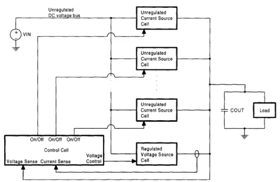
Figure 1.2: Unregulated current source cell.
passive component size, and in some cases makes it possible to integrate the passive compo-nents, either in silicon or as part of the printed circuit board. However, conventional dc/dc power converters cannot be operated at such high frequencies because of unacceptably large switching and gating losses, and the difficulty of realizing appropriate controls.
An excellent solution to this problem, developed in (3] and elsewhere, is to apply the topolo-gies and techniques associated with radio-frequency (RF) power amplifiers to dc/dc power converter design. In the work presented here, which builds upon the work shown in [1], a Class E RF power amplifier [5, 6, 7 and 8, chapter 13] is used as an inverter (Fig. 1.1) and combined with a gate driver, an impedance matching network, a compression network, and a rectifier to form a dc/dc converter cell that operates at 100MHz (Fig. 1.2). The unregu-lated dc input voltage is transformed by the cell to an unreguunregu-lated dc output current. Only on/off external control is required.
One or more such current source cells may be connected to the load in parallel with a voltage regulator to form a dc/dc voltage converter (Fig. 1.3). The voltage regulator maintains the desired load voltage. As the load varies, the current source cell or cells are modulated on and off to minimize the power demand on the voltage regulator. Because the voltage source output power is low, this source can be made physically small, relatively inefficient, and therefore inexpensive. To illustrate this fact, a linear regulator (rather than a switching sup-ply) can be used. The details regarding the interconnection and control of the unregulated
1.1 Introduction
Unregulated Unregulated
DC voltage bus Current Source
Cell V IN CU e Unregulated Caurrent Source Celll Un regulated
Current Source a fCOUToni[d
cell
On/Off On/Off On/Off
Control Cell Regulated
Voltage - - - Voltage Source Voltage Sense Current Sense Control Cell
Figure 1.3: Multiple current source cells used in parallel with a voltage regulator to form a dc/de converter with a regulated output voltage. The number of cells can be increased arbitrarily to increase output power level.
current source cells can be found in [1].
This converter topology has numerous merits, one of which is the high
fs
of the unregulatedcells. As a result, each cell requires only small capacitors (not more than a few hundred picofarads) and small air core inductors (not more than a few hundred nanoHenries), which makes the cell quite small, light and inexpensive. The absence of ferromagnetic inductor core material also makes the converter less sensitive to extreme ambient temperatures and mechanical stresses. Despite the high fs, the cell has low switching loss, and therefore requires relatively little heat sinking. The switch device chosen for the inverter is rated to dissipate enough power that no external heat sinking is required. High fs also allows each cell to be modulated at high frequency to respond rapidly to changes in load resistance. Another merit of this design is modularity. Because all of the unregulated cells are iden-tical, any number may be used in parallel to achieve a desired converter output power. This parallel architecture may also be used as a way of increasing converter reliability by preventing total converter failure in the event of cell failure. Finally, unlike many other dc/dc converter topologies, each converter cell has inherent short-circuit tolerance [8, page 366]. This is explained further in chapter 2.
-1.2
Thesis Objectives and Contributions
The goal of this thesis is to design, build, and test an RF dc/dc converter cell with improved performance over the cell described in [1]. Potential improvements include increased output power, increased efficiency, decreased board area and increased fs. To explore the possibility of making improvements in each of these areas, all segments of the converter are redesigned, including the inverter, gate drive, impedance transformation and compression stages, and rectifier.
Achieving improvements in the inverter entails a search for a more suitable switch device, including measurement and computer modelling of potential devices using PSPICE. Inverter performance is modelled for several candidate devices over the input voltage range and over a range of potential operating frequencies. The device that provides the best performance is chosen, and the effects of retuning for maximum efficiency or increased power are considered. Replacing the choke inductor with a discrete-component multi-resonant (MR) circuit to reduce switch voltage stress is also investigated here. Several inverter implementation issues, such as printed circuit board (PCB) design, inductor design, switch package inductance compensation and switch packaging, are considered.
A gate driver is designed to meet the requirements of the inverter's switch, which are different from the requirements of the device used in [1]. Gate drive tuning and PCB layout are discussed.
A matching network is used to match the input impedance of the compression stage to the impedance that the resonant inverter requires for efficient operation. Although a conven-tional network is used, it must be tuned to produce the most efficient inverter operation. Several tunings are calculated and compared through simulation.
A compression network is used to reduce the effect of load resistance variations on the resonant inverter operation. The theory of such a network is explained. An improved version of the basic compression network is designed for better management of harmonics. All aspects the rectifier design are discussed, including selection of rectification style (syn-chronous or diode), topology and switch device. The PCB layout of the rectifier is also discussed.
Once all parts of the converter are designed, the converter is built and measured in stages, and then characterized as a whole. All of the measurements made at the various stages are sensitive to the parasitic elements in the measurement equipment, and are limited by equipment voltage limits. Methods for making accurate measurements in spite of equipment
1.3 Organization of Thesis
non-idealities are discussed, as are methods of tuning certain converter stages to improve performance and to come closer to the simulated performance.
Because this thesis treats the design of every stage of the converter in detail, it makes significant contributions as a guideline for future RF converter design.
1.3
Organization of Thesis
In chapter 2, background information about the Class E topology is provided, along with a brief comparison of the Class E topology to other similar topologies (Class F, 1/F, etc.) Chapter 3 describes the inverter design, including the switch selection process, the selec-tion of an operating point, and the investigaselec-tion of alternative topologies. Chapter 3 also explains how the inverter is modelled using PSPICE. Chapter 4 explains the design of the self-oscillating gate drive circuit. Chapter 5 explains the theory and implementation of the impedance compression network. The design of the rectifier is detailed in chapter 6, includ-ing the process of selectinclud-ing appropriate diodes. Chapter 8 illustrates the purpose and design of the impedance matching network. The design of the printed circuit board is discussed in Chapter 9. Chapter 10 explains how the converter is constructed and measured. This chapter also analyzes the effects on overall efficiency and output power of tuning various parts of the converter. The thesis is concluded with chapter 11, where the contributions of this thesis are summarized, and potential future work is described.
-Chapter 2
Background
2.1
Introduction
This chapter provides background information about the structure and operation of the Class E amplifier, and compares it to other similar topologies (e.g. Class F, Class 1/F, etc.) to motivate the choice of the Class E topology. Each topology has distinct advantages over the others, such as lower voltage or current stress on the switch, or lower design complexity.
2.2
Class E Amplifier Operation
The Class E amplifier' (Fig. 1.1, [5, 6]) is powered by an unregulated voltage source in series with a choke inductor. Together, these provide nearly constant current to the rest of the amplifier while maintaining an average voltage at the drain equal to the supply voltage. The rest of the circuit can be viewed as two resonant tank configurations with a switch to
alternate between them. One tank configuration is the series combination of CR, LR and the load impedance, and dominates the behavior of the circuit when the switch is on. The other tank configuration is the series combination of C1, CR, LR and the load, and dominates when the switch is off. The resonant frequency of the first tank (switch closed, fCLOSED) is lower than that of the second tank (switch open, fOPEN), and the switch is operated at
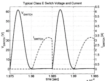
a frequency between the two tank frequencies (fs). This produces the harmonics necessary to create the typical Class E waveforms shown in Fig. 2.1. Of note in this figure is the fact that both the switch voltage and the derivative of the switch voltage are zero at the time of switch turn on. The voltage and current of capacitor C1 at turn-on are therefore both zero, creating zero voltage switching (ZVS) under ideal operation. Ideally, no energy is dissipated from C1 into the switch when it turns on, which facilitates operation at very high frequencies. Moreover, the low dv/dt at turn-on reduces the required speed of the gate
'To avoid confusion, the term amplifier is used to refer to the generic Class E circuit, and the term
inverter refers to the Class E circuit when used as a power inverter. The inverter is functionally the same as the amplifier, except that the design parameters are chosen with the inverter application in mind.
-Typical Class E Switch Voltage and Current VswTcH-SWITCH . ... ... - : ... . ... .... ... ... ... ... - I -. .. . - I 60 50 40-30 20 10 0 1.9 6.5 6 5.5 5 4.5 4 3.5 S 3 2.5_ 2 1.5 1 0.5 0 1.99 1.995 x 10⁻⁶
Figure 2.1: Typical Class E amplifier switch voltage and current waveforms with D = 50% and QL = 3.
drive circuitry.
As noted in chapter 1, the Class E topology inherently limits the current into the load under short-circuit conditions, because the tank impedance remains high due to LR and CR even with RLOAD = 0. This high tank impedance prevents the short circuit from appearing across the switch, which could destroy the choke.
The Class E topology also has several drawbacks, including high peak device voltage, high sensitivity to load impedance, and a dependence of output power on switch capacitance, which appears in parallel with C1. These drawbacks are discussed further in chapter 3. The values of C1, CR, LR and RLOAD are determined based upon the choice of fs, the
switch duty cycle (D), and QL. The choice of fs, D, and QL is discussed in chapter 3,
where equations for the passive components are given.
2.3
Alternatives to the Class E Topology
Several circuits similar to the Class E topology have been designed to trade off voltage and current peaking to reduce the required switch ratings. Unlike the Class E amplifier, these circuits contain filters to manage the higher order switch harmonics.
1.98 1.985
time [sec] 75
2.3 Alternatives to the Class E Topology
One such circuit is the Class F amplifier [9, 10], which suppresses the even switch voltage harmonics, and presents a high impedance to all odd harmonics, producing a square switch voltage under ideal operation. Because this minimizes switch voltage peaking, a switch with a lower voltage rating can be used in a Class F amplifier than in a Class E amplifier. At
D = 50%, the Class F maximum switch voltage is 2 times the input voltage, as compared to
the Class E factor of 3.56. The Class F topology also produces more sinusoidal switch current than the Class E amplifier, which results in greater RMS switch current and therefore in increased conduction loss.
The Class 1/F (or Class F inverse) amplifier [11, 12] allows only odd current harmonics to flow through the switch, which ideally produces a square switch current. The RMS switch
current, and consequently the conduction losses, are minimized. However, the required switch voltage rating is increased because of higher switch voltage peaking.
Any combination of even and odd voltage and current harmonics may be controlled to produce a desired tradeoff between voltage and current flattening, which is generally referred to as an E/F tuning (13].
One disadvantage of these topologies (F, 1/F, E/F, etc.) is their increased component count and design complexity compared to the Class E amplifier. Moreover, the benefit available from these circuits is limited by the characteristics of the available switch devices. As a result, neither full Class F nor Class 1/F is considered for this design. However, the use of a resonant network to provide some harmonic control is considered in section 3.8 as a means of increasing the switch voltage headroom slightly to protect the device.
-Chapter 3
Inverter Design
3.1
Introduction
This chapter describes the process of inverter design, and presents the necessary steps in the order that was found to be most efficient, beginning with a description of the design goals. The selection of an inverter topology is then explained, followed by an extensive discussion of switch device selection, which is especially important because switch non-idealities dominate converter loss. The processes of retuning the design to achieve higher efficiency or output power are then described, as is the process of reducing the choke inductor size to reduce the required PCB area. This chapter also considers the use of a discrete-component multi-resonant choke to reduce switch voltage peaking. Several other issues, such as switch package inductance compensation, switch packaging, and inductor design, are also treated.
3.2
Specifications and Goals
The first step in designing this inverter is to bound the design space by deciding which variables will be held constant, and which will be varied. This decreases the number of dimensions in the inverter design space, which simplifies the analysis of the tradeoff among output power, efficiency and inverter size. In this design, the constant parameters are the input voltage range, the duty cycle, and the loaded quality factor (QL) of the resonant tank composed of LR, CR and the RLOAD- QL is defined by Eq. 3.1 [7, page 150], where ws is
the switching frequency in radians per second, and fs is the same frequency in Hertz.
QL WSLR _ 2rrfsLR (3-1)
RLOAD RLOAD
Parameters such as the switching frequency and the capacitance across the switch are varied to explore design tradeoffs. This section explains why each of the parameters is either fixed
-or varied in this design.
3.2.1 Duty Cycle
Two of the important metrics of a Class E amplifier design are the peak-to-dc ratio of the switch voltage, V YDC , and the peak-to-dc ratio of the switch current, I IDC [7, pages 154-155].[,pgs1 These quantities are proportional to the amount of energy that is lost in parasitic resistances due to the oscillation of energy through passive components. These ratios are also measures of switch stress, and should be minimized for both reasons. A duty cycle of 50% is chosen for this design because it minimizes the union of the two ratios, thereby maximizing the power-output capability [8, pages 356-357]. A 50% duty cycle is also easier to achieve at high frequency than a very small or very large duty cycle.
3.2.2 Loaded
Q
FactorQL is chosen to obtain the desired tradeoff between output sinusoidal purity and low peak switch current. In power amplifier applications, high QL is selected such that the voltage across the load is as sinusoidal as possible. This produces narrow-band amplification, which is useful in communication applications. However, high QL also produces a large ratio of peak-to-dc switch current. This corresponds to a higher RMS switch current, and therefore to greater switch conduction losses and passive component parasitic resistance losses. In an inverter application, the spectral purity of the output voltage is not as important as efficiency, and QL can be sized to give low tank loss. QL = 3 is chosen for this design based upon the plots given in [7, page 154].
3.2.3 Input Voltage Range
An input voltage range of 11 to 16V is chosen to make the converter compatible with conventional automotive systems and other 12V battery applications. Since the peak switch voltage in the Class E topology is about 3.6 times the input voltage (given a 50% duty cycle [8, page 362]), this design requires a device rated for at least 57.6V. To allow for sufficient switch headroom, only devices rated for 65 or 70V (industry standard values for communications devices at the time of writing) are considered for this design.1 A peak
3.3 Switch Device Comparison Using Datasheet Information
switch voltage of ~ 60V is convenient because most of the next smaller available switch devices are rated for 40V, and the next larger devices are rated to 100V.
3.2.4 Operating Frequency
The switching frequency fs is selected to accommodate the strong interaction between frequency and both efficiency and output power. It was considered desirable, but not essential, that fs be at least 100MHz to match or exceed the operating frequency of the previous design [1]. This ensures that the energy storage requirements are not greater in this design than in the previous design.
3.2.5 Efficiency, Output Power, Physical Size
Exact specifications are not set for inverter efficiency, output power and board size because these variables are governed primarily by switch non-idealities, such as on-state resistance, output capacitance and package size. At the time of writing, the evolution of appropriate switch devices is so rapid that hard limits placed on these variable can become obsolete in a few months.
3.3
Switch Device Comparison Using Datasheet Information
This section explains the process of identifying viable switch devices for the inverter. Selec-tion of a switch is of foremost importance in this inverter design because the non-idealities of currently available devices are strong limiting factors for inverter efficiency, output power, size, and controllability. It is therefore advantageous to compare a variety of switches avail-able from different manufacturers to find a device that will produce the best tradeoff among inverter efficiency, output power, and size.
3.3.1 Selection of Devices
A variety of RF power transistors could be considered for this design, including Lateral Double-diffused MOS (LDMOS) devices, Vertical Double-diffused MOS (VDMOS) devices, and bipolar devices. However, most power VDMOS devices cannot be operated efficiently at or above 100MHz because of high gating loss due to large gate-source and gate-drain
-Drain CRSS
Gate ooCOSS
CISS
Source
Figure 3.1: A simplified view of the connection of parasitic capacitances in an LDMOS device.
capacitances. These capacitances are greater in vertical devices than in lateral ones because vertical devices have larger overlap between the gate and drain diffusion and between the gate and source diffusion [14] [15, page 227, Fig. 2]. Bipolar devices also have high gating losses due to their finite current gain. A more detailed comparison of bipolar and LDMOS devices is given in [16].
As a result of the drawbacks of bipolar and VDMOS devices, the decision was made to limit the device search primarily to LDMOS devices. LDMOS offers a combination of low on-state resistance (RDSON), low output capacitance (Coss), and low input capacitance (Ciss), which results in high efficiency inverter operation at very high frequencies, as explained below. The capacitances Coss and CISS are shown, along with the reverse capacitance
CRss, in Fig. 3.1.
Minimizing RDSON reduces inverter conduction loss, increasing inverter efficiency. Ideally, this parameter should be zero, since no aspect of converter performance is improved by RDSON- CISS should also be minimized to reduce gating loss. As CIss is decreased, less
charge must be moved on and off of the gate in each cycle. Since the gate charge moves through the gate resistance and the gate drive circuit parasitic resistances, moving less charge on and off of the gate results in a higher gate-drive efficiency.
As Coss increases, the amount of energy that resonates through Coss to the load in each cycle is increased. Similarly, as fs is increased, more energy is transferred to the load per unit time. Inverter output power is therefore proportional to both Coss and fs. Thus, lower values of Coss allow fs to be raised without increasing output power. This allows efficiency to be kept constant as fs is increased, since output power is proportional to current, and passive component loss is proportional to current squared. External capacitance (CEXTRA) can be added from drain to source if a higher output power level is desired at a given fs. This has several benefits over higher Coss.
3.3 Switch Device Comparison Using Datasheet Information
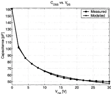
The most obvious benefit is that adding external capacitance affords greater design flex-ibility, because external capacitance can be added with only a slight modification to the tuning of the resonant circuit. This allows the inverter operating point to be changed after a switch has been chosen, and even after the printed circuit board has been laid out. In this design, 20pF is added from drain to source in the final design to achieve the desired output power level, which means that the board space requirement increases only slightly. Additionally, discrete capacitors have a higher quality factor than the intrinsic LDMOS output capacitance. Consequently, inverter operation is more efficient with a given amount of external capacitance than with the same amount of internal capacitance.
Finally, the fixed external capacitance causes less peaking of VDS than a comparable amount of additional internal Coss. This is attributable to the nonlinear relationship between Coss and VDS [17, 18], governed by equation 3.2 where Cj, is the value of Coss at VDS = OV, V is the built-in junction potential, and M is the grading coefficient. These three constants are determined as explained in section 3.4.3.
Coss = CMO (3.2)
When the switch turns off, VDS rises due to the oscillation of the resonant tank. As VDS becomes larger, Coss becomes smaller. Since the current in Coss is roughly constant, the smaller value of Coss causes an increase in the slope of VDS, as governed by the constitutive equation for a capacitor. This causes VDS to rise more than it otherwise would, thereby decreasing Coss further. An inverter with a larger value of Coss and no external capacitance has significantly less voltage headroom than an inverter with low Coss and fixed external capacitance. To demonstrate this, two inverters are compared in simulation (see appendix A.4). Both inverters use the switch that was chosen for the final design. In the first inverter, Cj, is increased by 20pF from its measured value, and no Coss is added. In the second inverter, CjO is kept at its actual value, and 9.6pF of extra capacitance is added such that the inverters have the same output power to within 1mW, and the same efficiency to within 0.01%. The inverter with added external capacitance has a peak voltage that is lower by 2.86V than the 70.28V peak of the other inverter.
Because of the benefits of low RDSON and low Coss, as described above, LDMOS devices with a low product of RDSON and Coss are sought in the device search. When two devices are compared based upon their RDSONCOSS products at a given value of VDS, the device with the lower product will operate the inverter more efficiently. To form the product, RDSON in ohms and Coss in picofarads are used, such that a device with RDSON = 10OMQ
-Drain RGATE
Gate )--,1 D S
Coss
Ciss- RBIG (Ideal
(100k
RDSON
Source
Figure 3.2: Layout of the PSPICE LDMOS model used to compare candidate LDMOS devices based upon datasheet information.
and Coss = 10pF has an RDSONCOSS product of 1. CISS is not considered until the device selection is narrowed down because it is typically on the same order of magnitude as Coss. Appendix B contains information about all of the LDMOS devices that were identified in this device search. This appendix also includes a table that contains information about a number of VDMOS devices. Almost all of the VDMOS devices have a lower RDSONCOSS product than the LDMOS devices, which supports the decision to focus on finding LDMOS devices for use in this inverter design.
3.3.2 PSPICE Modelling with Datasheet Information
Comparison of devices based upon the product of RDSON and Coss gives an estimate of how efficiently devices will perform relative to one another. To get absolute estimates of inverter efficiency and output power with a given device, simulations can be performed in software such as PSPICE using information obtained from device datasheets. This saves time
and money by eliminating certain devices from consideration before samples are ordered and characterized. This section describes how LDMOS devices and the passive components in the inverter can be modelled using datasheet information. Section 3.3.3 then explains how these models can be used in simulations. A schematic of the switch model is shown in Fig. 3.2, and a schematic of the entire inverter is shown in Fig. 3.3. The netlists for these
simulations are given in appendix A.5.
For each candidate LDMOS device, Coss is modelled as a fixed capacitance, rather than a nonlinear capacitance governed by equation 3.2. This is because some datasheets give Coss only at a single voltage, and a fair comparison is attained by using the same type of information for all candidate devices. The equity of this comparison is increased by the fact that most manufacturers of 65 and 70V LDMOS devices specify Coss in the range
3.3 Switch Device Comparison Using Datasheet Information
...
... ... LR R
VIN (13) DMORLOAD
device
VSWITCH (sine) model
Figure 3.3: Structure of the PSPICE inverter model used to compare candidate LDMOS devices based upon datasheet information.
26 to 28V. The change in Coss over this range is quite small. As an illustration of this fact, consider that the datasheet for the Freescale MRF373ALSR1 (appendix B) shows
Coss decreasing by about 0.5pF from 26 to 28V. By comparison, the other devices under consideration have Coss values that differ from that of the MRF373ALSR1 by tens of picofarads.
The value of CIss is also taken from the datasheets, where it is typically specified at the same voltage as Coss. Like Coss, CIss is a nonlinear capacitance. However, CIss changes very little over the VDS range of interest. As a result, CIss is considered constant, and its
nonlinearity is not measured in the device characterization described in section 3.4.
RDSON is given in the datasheets either explicitly, or as VYsf, . The values of the gate
resistance (RGATE) and the equivalent series resistance of Coss (Rscoss) are not typically
given in the datasheet, but are set at 300mQ for all candidate devices based upon typical values for LDMOS devices. Estimating these values gives more accurate simulated estimates of efficiency and output power.
The diode Dsw shown in Fig. 3.2 is ideal, and is intended to model the ability of the LDMOS device to carry current only in the forward direction. The switch Si has a gain of over 126, which is appropriate because the device is driven as a switch instead of as an amplifier. As indicated in [19, page 2-97], the gain should not be made too great, or numerical problems may arise. The switch is set to have a very low on-state resistance, such that the resistance
RDSON dominates the on-state resistance of the model, and a very high off-state resistance
of 1OIQ. The high off-state resistance is appropriate because typical LDMOS devices have an RDSOFF which is on this order of magnitude (see Tables D.4 and D.5 in appendix D.3). Also of note is the absence of a body diode in the LDMOS model. Unlike vertical devices, lateral devices do not have a parasitic diode from source to drain.
The simulated inverter circuit, shown in Fig. 3.3, includes the LDMOS model described
-above, and passive components with non-idealities modelled as described here. The ca-pacitor CR is modelled with a
Q
of 3000, based upon the datasheets for Cornell-Dubilier Electronics (CDE) surface mount mica capacitors. The inductor LR is modelled using aQ
of 120 at 150MHz, which is typical for Coilcraft Mini Spring and Midi Spring surface mount inductors. For the choke inductor LCHOKE, the dc resistance of 90mQ is modelled along with theQ
of 104 at 50MHz. The datasheets for the inductors and capacitors are shown in appendix G.To reduce the complexity of the circuit at this preliminary stage in the inverter design, the LDMOS device is driven with an ideal sinusoidal voltage source, instead of with a self-resonant gate drive. The peak voltage of this source (18V) is approximately the voltage that the self-resonant driver would apply to the gate, which gives a good approximation to gate loss for each candidate device.
3.3.3 Inverter Performance Comparison Using PSPICE Simulation
Once the candidate LDMOS devices and the inverter passive components are modelled, inverters can be designed at a range of frequencies and with a number of different devices. The tank components are selected using Eq. 3.3 from tabular results in [7] with D = 50%, QL = 3, no CEXTRA, and fs from 100 to 240MHz:
0.2150 RLOAD = 2150 (3.3a) 27r fsCDS CR - 0.4166 27rfsRLOAD LR = 3.7 ORLOAD (3.3c) 27rfs
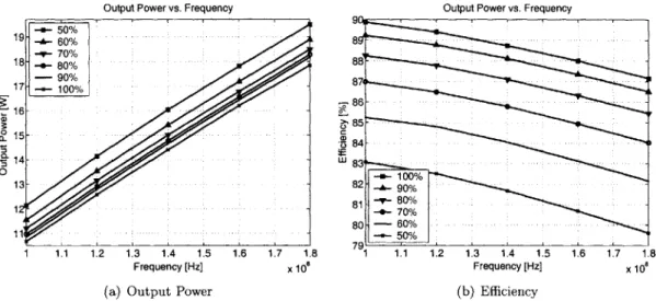
This set of equations is implemented as functions in PSPICE to automatically generate Class E tunings at a range of frequencies. Transient simulations are performed with a stepping of the switching frequency, and efficiency and output power are plotted versus frequency (Fig. 3.4). These plots allow the designer to decide which devices to purchase for further characterization and simulation.
Based upon the data shown in Fig. 3.4, it was decided that the MRF373ALSR1 and the MAPLST0810-030CF should be obtained and characterized. The AGR09080GUM was also obtained, but was not characterized because it has a packaged area of 3.14 times that of the M/A-COM and Freescale device packages. It was also decided that an operating frequency
3.4 Switch Measurement and Modelling Efficiency vs. Frequency 2 2.2 2.4 x 10⁸ -- Freescale MRF373ALSR1 -4- M/A-COM MAPLST0810-030CF ST PD57018 --Agere AGRO9030GUM 1111 4 11 .... ... .... ..-... ....
Output Power vs. Frequency
40 35 30 25 0 m 20 0 15 10 1 1.2 1.4 1.6 1.8 2 2.2 2.4 Frequency [Hz] x 108 (b) Output Power
Figure 3.4: Simulated inverter output power and efficiency vs. frequency for four LDMOS devices using datasheet information. The ST device was used in the first converter, and is shown for reference. VIN = 16V. Plots include gate losses with ideal sinusoidal voltage source drive.
between 100 and 160MHz would provide the most desirable performance. As can be seen from Fig. 3.4, the maximum inverter efficiency for each device falls within this frequency range (or below, where the passive components become larger than those used in [1]).
3.4
Switch Measurement and Modelling
This section describes the process of measuring certain ac and dc characteristics of the candidate LDMOS devices. These measurements are made both to verify the datasheet information and to obtain more information needed to model the devices more accurately in PSPICE. The measured parameters are Coss, CIss, the ESR and ESL associated with
Ciss and Coss, and RDS. The gate threshold voltage is estimated based upon the RDS
measurement, as is RDSON.
3.4.1 Measurement of ac Characteristics
The ac measurements are made with an Agilent 4395A in impedance analyzer mode. An Agilent 43961A RF impedance test adapter is connected to the analyzer, and an Agilent 16092A spring clip fixture is connected to the adapter. An external dc power supply is
- 35 -93 92 91 ) wU 90 898-86 - - gr GO00U 87. 7
Agr- re7GR APLST010-030CF
85. - Freescale MRF373ALSR1
-e-- ST PD57018
1 1.2 1.4 1.6 1.8
Frequency [Hz] (a) Efficiency
connected via coaxial cable to the adapter, and a digital volt meter (DVM) is connected at the output of the dc supply. The impedance analyzer calibration is done with the dc supply connected and set to zero, and with the DVM connected. An averaging factor of four is used to average out noise. The intermediate frequency bandwidth is low (30Hz) to achieve accurate representation of the sharpness of the self-resonant points of CIss and Coss, which allows accurate measurement of the impedance at this point. This impedance is the equivalent series resistance (ESR) of the given capacitance [20, pages 305-307]. The frequency sweep begins at 500kHz to allow accurate measurement of CIss and Coss without including the effect of the self-resonance of these capacitances. The sweep goes up to 500MHz to allow the self resonant point (and therefore the ESR) of Ciss and Coss to be measured accurately, since this point occurs at nearly 500MHz for some devices. The upper frequency limit is also high because measurement of the equivalent series inductance (ESL) of these capacitances requires impedance information for frequencies above the self-resonant point.
To measure Coss, a short is soldered from gate to source, and a series capacitance mea-surement is made from drain to source at 1MHz, which is more than two decades below the self resonant frequency. VDS is stepped from OV to the voltage at which Coss is specified in the datasheet. Measurement of the M/A-COM MAPLST0810-030CF is accurate to within 4.65% of the datasheet value, and measurement of the Freescale MRF373ALSR1 is accurate to within 1.95%.
The ESR and ESL are measured with an impedance magnitude measurement and a series RLC equivalent circuit model. This measurement is made only with VDS = OV, because the decision was made to simplify the PSPICE model by ignoring any voltage dependence in ESR and ESL.
Similarly, CIss is measured only at VDS = OV, despite the nonlinear dependence of CIsS on VDS. One reason is that CIss changes very little with voltage as compared with Coss, and can therefore be reasonably approximated as constant. Furthermore, measuring gate to source capacitance with a drain to source voltage connection requires three terminals. Since the measurement fixture has only two terminals, the voltage connection would need to be made at the device under test (DUT), and the wire for this connection would intro-duce far more noise than the coaxial connection made to the adapter from the dc supply. Furthermore, the effect of this type of measurement setup on the test fixture is unknown. To keep VDS = OV, a short is soldered from drain to source. The capacitance CIss, the ESR and the ESL are measured using the impedance analyzer as described for Coss. Shorting the drain to source to measure CIss has the drawback that the reverse capacitance
3.4 Switch Measurement and Modelling
independently. However, this is unimportant for the measurement of Ciss since CRSS is much smaller than Ciss for the switches being considered. For example, the CRSS is 2.03% of CIss for the Freescale MRF373ALSR1, and 2.4% of CISS for the M/A-COM MAPLST0810-030CF. CRSS is small enough that it is not even estimated in the PSPICE model.
All of the impedance analyzer measurements are shown in appendix D.2.
3.4.2 Measurement of dc Characteristics
To measure RDS as a function of VGS, a digital ohmmeter is connected from drain to source, and a dc supply is connected from gate to source. The gate to source voltage is stepped from zero to within a few volts of the maximum gate to source voltage, and the resistance is recorded at each step, along with the measured value of VGS- To improve measurement ac-curacy, the resistance of the test setup is measured with both measurement leads connected to the same lead of the DUT. This is an attempt to account for all of the contact resistances involved. The resulting test setup resistance measurement is subtracted from the measured values of RDS. The resistance data for both the M/A-COM MAPLST0810-030CF and the Freescale MRF373ALSR1, along with more detailed information about the measurement setup, is provided in appendix D.3. The measured and datasheet-specified values of RDS are compared at the value of VGS for which RDS is specified. For the MAPLST0810-030CF, the measured value of RDSON is greater than the specified typical RDSON value by 30% to 60%, depending upon measurement variations, while for the MRF373ALRS1, RDSON is
10% to 54% greater than the specified typical
RDSON-Four-wire resistance measurements are also made of these devices in an attempt to reduce the discrepancy between the measured and specified values of RDSON. Two short wires of equal length are soldered to the drain terminal, and two more to the source terminal. These wires are also connected to an HP 34401A digital multimeter by banana plugs. The gate voltage is brought to the DUT with alligator clip lines, and the voltage VGS is measured at the DUT. Using this technique, the RDSON of the M/A-COM part is found to be 296mQ, or 48% greater than the datasheet-specified typical value, and the RDSON of the Freescale
part is found to be 146mQ, or 6.83% greater than the specified typical value.
The fact that the four-wire measurements do not yield significantly improved results suggests that the (devices should be measured under the same conditions specified in the datasheets. This involves forcing significant drain current through the device (3A for the Freescale MRF373ALSR1 and 1A for the M/A-COM MAPLST0810-030CF) at the specified VGS and measuring the resulting VDS. A curve tracer would be well suited to this type of