HAL Id: hal-02908981
https://hal.archives-ouvertes.fr/hal-02908981v2
Submitted on 8 Jun 2021HAL is a multi-disciplinary open access
archive for the deposit and dissemination of sci-entific research documents, whether they are pub-lished or not. The documents may come from teaching and research institutions in France or
L’archive ouverte pluridisciplinaire HAL, est destinée au dépôt et à la diffusion de documents scientifiques de niveau recherche, publiés ou non, émanant des établissements d’enseignement et de recherche français ou étrangers, des laboratoires
Plasmon-Driven Hot Electron Transfer at Atomically
Sharp Metal-Semiconductor Nanojunctions
Masiar Sistani, Maximilian Bartmann, Nicholas Güsken, Rupert Oulton,
Hamid Keshmiri, Minh Anh Luong, Zahra Sadre Momtaz, M. den Hertog,
Alois Lugstein
To cite this version:
Masiar Sistani, Maximilian Bartmann, Nicholas Güsken, Rupert Oulton, Hamid Keshmiri, et al.. Plasmon-Driven Hot Electron Transfer at Atomically Sharp Metal-Semiconductor Nanojunc-tions. ACS photonics, American Chemical Society„ 2020, 7 (7), pp.1642-1648. �10.1021/acsphoton-ics.0c00557�. �hal-02908981v2�
This document is the unedited Author’s version of a Submitted Work that was subsequently accepted for publication in ACS Photonics, copyright © American Chemical Society after peer review. To access the final edited and published work see [https://pubs.acs.org/articlesonrequest/AOR-2WPNUDHCUUFTYKTFR8T5]
Plasmon-Driven Hot Electron Transfer at
Atomically Sharp Metal-Semiconductor
Nanojunctions
Masiar Sistani1, Maximilian G. Bartmann1, Nicholas A. Güsken2, Rupert F. Oulton2,
Hamid Keshmiri1, Minh Anh Luong3,Zahra Sadre Momtaz4,
Martien I. den Hertog4, Alois Lugstein1
1 Institute of Solid State Electronics, Technische Universität Wien, Gußhausstraße 25-25a, 1040 Vienna, Austria 2 The Blackett Laboratory, Department of Physics, Imperial College London, London SW7 2AZ, United Kingdom 3 Univ. Grenoble Alpes, CEA, INAC, MEM, F-38000 Grenoble, France
E-Mail Address of corresponding author: [email protected]
ABSTRACT
Recent advances in guiding and localizing light at the nanoscale exposed the enormous potential of ultra-scaled plasmonic devices. In this context, the decay of surface plasmons to hot carriers triggers a variety of applications in boosting the efficiency of energy-harvesting, photo-catalysis and photo-detection. However, a detailed understanding of plasmonic hot carrier generation and particularly the transfer at metal-semiconductor interfaces is still elusive. In this paper, we introduce a monolithic metal-semiconductor (Al-Ge) heterostructure device, providing a platform to examine surface plasmon decay and hot electron transfer at an atomically sharp Schottky nanojunction. The gated metal-semiconductor heterojunction device features electrostatic control of the Schottky barrier height at the Al-Ge interface, enabling hot electron filtering. The ability of momentum matching and to control the energy distribution of plasmon-driven hot electron injection is demonstrated by controlling the interband electron transfer in Ge leading to negative differential resistance.
KEYWORDS
Plasmonic-metal nanostructures have become a powerful tool to concentrate and manipulate light below the diffraction limit, paving a pathway to couple optical energy effectively to nanoscale systems.1,2,3,4 The plasmonic manipulation of light in metal-semiconductor (M-S) heterostructures
became of particular interest due to their capability of generating hot electrons in the metal that can be transferred to the semiconductor and facilitate chemical reactions.5 The selection of
momentum matched materials6 and the design of optimized device architectures are thereby
important for controlling plasmon-induced optical field distribution,7 hot electron injection8 and
energy transfer at a M-S heterojunction.9 Propagating surface plasmons approaching a M-S
interface can decay either radiatively10 via scattering of photons or non-radiatively through the
generation of hot carriers.11 For radiative decay, photons are scattered from the metal into the
adjacent semiconductor driving electron-hole pair generation commonly denoted internal photogeneration.12,13,14,15,16 However, this mechanism is limited to energies above the
semiconductor band-gap7 and for Ge due to the indirect bandgap the small electron-photon
cross-section makes this process inherently inefficient.17 For non-radiative plasmon decay,
plasmon-driven electrons that simultaneously move toward the planar interface while also having sufficient kinetic energy to overcome the Schottky barrier, may be directly injected into the semiconductor.17
These injected hot electrons exhibit a rather broad energy distribution, which stems from the almost continuous density of electronic energy states that exist below the Fermi level of metals.15
However, assuming excitation of electrons at the Fermi level, the maximum energy of the injected hot electrons is 𝐄 = ℏ𝛚𝐒𝐏𝐏,7,17,18 with 𝛚
𝐒𝐏𝐏 being the surface plasmon polariton (SPP) angular
frequency.8 Injection efficiencies less than 1% are expected due a range of limiting processes
reflection at the M-S interface.19 Contributing to applications such as plasmon enhanced
photo-catalysis,5 light harvesting9 and photodetection,11 we extend the vast body of pioneering work on
experimental investigations on plasmon decay to hot electrons,7,17,20,21,22 by introducing a gated
metal-semiconductor heterojunction device features electrostatic control of the Schottky barrier height at the Al-Ge interface, enabling hot electron filtering.
RESULTS AND DISCUSSION
In this work, we investigate surface plasmon-driven electron transfer processes at an atomically sharp M-S nanojunction of a monolithic Al-Ge nanowire (NW) heterostructure. Figure 1a and b show the schematic and a false-color scanning electron microscopy (SEM) image of the gated plasmon transfer device (GPTD) comprising a focused grating coupler (FGC) to launch SPPs in the single crystalline Al (c-Al) NW plasmon waveguide attached to the semiconducting Ge segment. An omega-shaped gate electrode directly atop of the atomically sharp heterojunction enables electrostatic control of the Schottky barrier at the M-S interface.24 The device is realized
on a 40 nm thick Si3N4 membrane25 by a thermally induced exchange reaction between
single-crystalline Ge NWs covered by a passivating Al2O3 shell and lithographically defined Al contact
pads resulting in crystalline Al-Ge-Al NW heterostructures. More details regarding the Al-Ge heterostructure formation are described in the work of Kral et al.26 and El Hajraoui et al.27 The
high angle annular dark field (HAADF) scanning transmission electron microscopy (STEM) images in Figure 1c-e show the monolithic Al-Ge-Al nanowire heterostructure with atomically sharp interfaces enwrapped by a 20 nm thick passivating Al2O3-shell.
Figure 1. (a) Schematic illustration of the top-gated Al-Ge NW heterostructure device fabricated on a 40 nm thin Si3N4 membrane. (b) False color SEM image of the GPTD device. The FGC atop
of the Si3N4 membrane is schematically indicated with dashed lines. Scale bar is 1 µm. (c) HAADF
STEM image of the entire Al-Ge-Al NW heterostructure comprising a Ge segment length of LGe =
600 nm and a diameter of dNW = 40 nm enwrapped by a 20 nm thick Al2O3 shell. Scale bar is 200
nm. TEM images showing (d) the entire Al-Ge interface of the NW heterostructure (scale bar is 40 nm) and a zoomed-in image where the Ge region is oriented on the [110] zone axis (scale bar is 5 nm).
Effective surface plasmon excitation is achieved by coupling normal incident TM polarized laser with a vacuum wavelength of λ = 532 nm into the c-Al NW waveguide using a Si3N4 membrane
FGC,28 located above the Al contact pad (see Figure 1a and 1b).29 As previously shown, for such
a configuration we experimentally determined a SPP propagation length of LSPP = 140 nm at λ =
Time Domain (FDTD) simulations revealed that adding the omega-shaped gate atop the Al-Ge nanojunction significantly lowers the LSPP (see Figure S1).
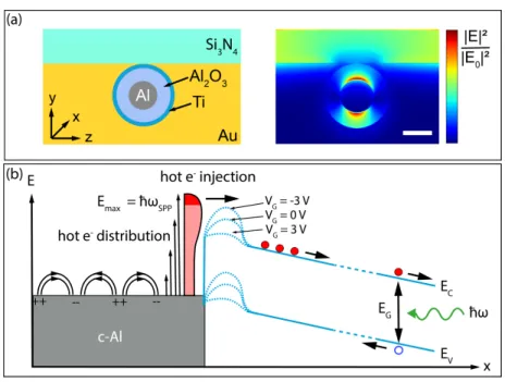
Figure 2a shows a cross-sectional schematic of the Al plasmonic waveguide enwrapped by the Al2O3 shell and the omega-shaped metal gate. FDTD simulations confirm a bound mode
propagation along the NW, below the gate and right until the Al-Ge interface. Here, the entire propagation pathway of a TM polarized incident beam coupled via the FGC to the c-Al-NW and the gated Al-Ge NW junction was considered. Figure 2a shows the field intensity distribution of the coupled light in close vicinity to the gated Al-Ge interface where hot carriers are excited. The individual field intensity distributions |Ex|², |Ey|², |Ez|² are shown in Figure S2. Additional field
intensity distributions at λ = 1100 nm, 1500 nm and 1800 nm are illustrated in Figure S3 for comparison. Further, Figure S4 shows a field intensity cross-section of the gated Al-Ge nanojunction in the xz-plane for an excitation of λ = 1100 nm. The simulation shows clearly the feasibility of plasmon guiding below the gate electrode and plasmon decay at the Al-Ge interface. The omega-shaped top gate at the M-S interface enables tuning of the Schottky barrier height at the M-S heterojunction. In fact, the electrical characteristic of the heterojunction can be tuned between Ohmic and Schottky behaviors (Figure S5). According to the schematic in Figure 2b, only hot electrons that move toward the nanojunction with sufficiently high energies overcome the barrier and enter the Ge segment, following nonradiative SPP decay. According to the work of R. Sundararaman et al.,7 we assumed a continuous hot electron energy distribution reaching from the
Fermi level of Al to the maximum energy 𝐄 = ℏ𝛚𝐒𝐏𝐏 (see schematic in Figure 2b). By applying
a bias voltage (VBias), as shown in Figure 1a, for a given barrier height, these injected charge
plasmons by direct electrical means,23,30 and even tune the energy of the electrons surpassing the
Schottky junction of this M-S plasmon detector.
Figure 2. (a) Illustration of the gated c-Al NW segment cross section in the vicinity of the Al-Ge nanojunction indicating the different material layers surrounding the NW. The according simulated distribution of the normalized electric field intensity (|E|2/|E
0|2) in direct vicinity to the
Al-Ge interface of the fundamental mode is shown on the right. The individual field contributions |Ex|², |Ey|², |Ez|² are illustrated Fig. S2. Here, coupling of TM polarized light via the FGC (λ = 532
nm) is considered. The simulations show that the mode is bound to the c-Al NW even below the gate. The scale bar is 40 nm. (b) Schematic illustration of SPP propagation along the c-Al NW, SPP decay induced carrier injection into the Ge segment and the band-diagram with gate dependent barrier height. The green arrow schematically shows photoexcitation of the Ge segment and the associated electron-hole pair generation.
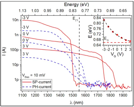
To demonstrate the mode of operation of the electrostatically tunable barrier, which works as an
energetic filter for plasmon-driven hot electron injection, we performed wavelength dependent measurements. A tunable laser was focused on the FGC and the plasmon-driven hot
electron transfer was investigated measuring the SP-current through the GPTD as a function of the gate potential. Figure 3 shows a comparison of the SP-current (red) with the photo-current (current) induced by directly focusing the laser onto the Ge segment (blue dotted curves). A PH-current only occurs for photon energies slightly higher than the direct bandgap (EΓ1) and appeared
to be independent of the gate voltage. A SP-current occurs for both interband excitation as well as plasmon-driven hot electron injection, which is tunable by the gate voltage (within the physical limit of the gate dielectric) from about 1500 nm to about 1850 nm. For increasing gate voltage, corresponding to a lowering of the Schottky barrier height, less energetic electrons can surpass the junction and contribute to the SP-current, even when the photon energy coupled into the c-Al waveguides is below the direct bandgap energy of Ge (0.8 eV). This sub-bandgap photodetection rules out a mechanism based upon direct photogeneration at the M-S interface.
Assuming that the plasmon-induced near field drives the hot electron generation,7,17 the maximum
wavelength where SP-current can still be measured for a certain gate voltage, indicates both the maximum energy of injected electrons into the Ge as well as the Schottky barrier height. Thus, the inset in Figure 3 shows the calculated effective barrier heights for plasmon-driven hot electron transfer from the c-Al waveguide into the Ge detector as a function of the gate voltage. The thereof, estimated injection efficiencies according to Fowler’s theory31 for gate voltages of V
G = -3 V, 0 V
of limiting processes including, ultra-fast carrier-carrier relaxation,5 the lack of vertical momentum
of hot electrons and reflection at the M-S interface.19
Figure 3. Spectral response of the SP- and PH-current for a bias voltage of VBias = 10 mV and
gate-voltages between -3 V and 3 V. The inset shows the thereof evaluated energy of hot electrons extracted from wavelength dependent measurements of the SP-current.
The ability to control the energy and momentum of plasmon-driven hot electrons injected into the Ge enables us to induce negative differential resistance (NDR),32 an effect that may be used for
fast switching logic circuits, static memory cells, or high-frequency oscillators.33 NDR can arise
from electrons with sufficiently high energy being scattered to a heavy mass valley with a lower mobility, thus increasing the resistivity of the Ge.34 This so-called transferred electron effect has
been observed at high electric fields in numerous systems, perhaps best known as the Gunn-effect in GaAs35 but also GaN nanocrystals36 and Ni/Ge Schottky diodes.37
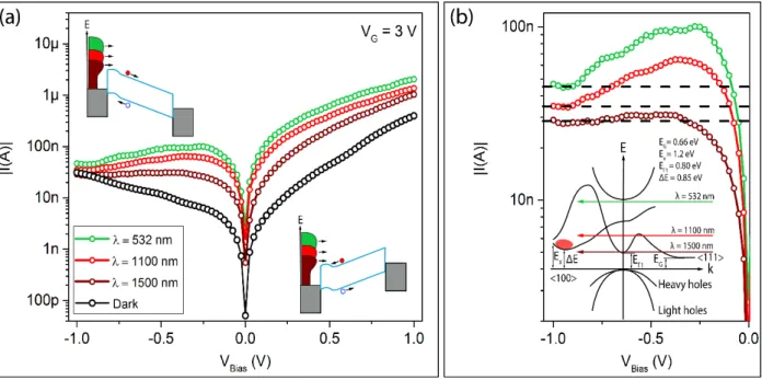
To investigate such SPP momentum induced NDR in Ge, the GPTD was operated as a Schottky barrier field effect transistor (FET). The black curve in the semi-logarithmic plot of Figure 4 shows the I/V characteristic with the drain current 𝐼 ∝ exp(𝑒𝑉/𝑘#𝑇), which is typical for semiconductor NW devices with two back-to-back Schottky contacts.38 The rectifying behavior is a direct
consequence of different barrier heights of the M-S junctions interfacing the NW. 39,40,41 The
SP-currents with laser illumination at the FGC at λ = 532 nm, λ =1100 nm and λ =1500 nm are shown in green, red and dark red respectively. For a gate voltage of 3 V and thus low Schottky barrier height, plasmon-driven hot electrons are effectively injected into the Ge segment, thus inducing a large SP-current. At positive bias voltages we observed a steady SP-current increase for all three wavelengths. The injected hot electrons arising from the plasmon decay at the Al-Ge interface are moving against the electric field and undergo thermalization via electron and electron-phonon scattering as well as electron-hole pair generation (see lower inset in Figure 4).42 These
additional charge carriers are swept out from the Ge segment driven by the electric field and contribute to the overall current through the FET. For negative bias, NDR is observed, with a maximum peak to valley ratio of 2.3 for the SP-current recorded for plasmon excitation with a laser wavelength of λ = 532 nm (green curve). Note that for negative bias the plasmon-driven hot electrons are injected with a momentum aligned to the electrical field in the Ge segment and are thus accelerated (upper inset).
According to the Ridley-Watkins-Hilsum theory37, NDR via an electron transfer process requires
semiconductor. This holds for Ge as the energy difference between the L-point and Δ-point minima of the ⟨111⟩ and ⟨100⟩ sub-bands of ΔE = 0.19 eV38 is significantly higher than the thermal energy
at room temperature (kBT= 25.8 meV) but much less than the bandgap (EG = 0.66 eV) (inset of
Figure 4b).38 To finally achieve NDR, it is required that electrons in the lower valley have a lower
effective mass than those in the upper valley.35 For Ge the transverse effective electron mass in
the Δ-point m*Δ,t = 0.288 m0, is significantly higher than that in the L-point minimum, m*L,t =
0.082 m0.43 Although the Γ-point minimum is energetically closer to the L-point minimum, the
coupling constant between the 111 and 000 minima is significantly lower than between the 111 and 100 minima.43 Thus, the transfer of electrons mainly occurs from the L-valley to the Δ-valley
and the respective energy difference of ΔE = 0.19 eV38 determines the threshold electric field for
electron repopulation. Hot electrons arising from the plasmon decay at the Al-Ge interface are already at a higher energy level and require only moderate electric fields to overcome a smaller energy difference to be scattered to the Δ-valley. Accordingly, the NDR effect fades out as the energy of the hot electrons declines for exciting the FGC with laser light at λ = 1500 nm. Therefore, the maximum energy of injected hot electrons (0.82 eV) is not sufficient anymore to inject electrons effectively into the Δ-valley.
It is important to note that our measurements provide substantial experimental evidence that the momentum of hot electrons originating from surface plasmon decay is suitable for scattering into the lower mobility Δ-valley of Ge. In contrast, no signs of NDR could be found for directly focusing the laser onto the Ge segment (see Figure S7).
Figure 4. (a) Dark current and SP- current recorded for excitation wavelengths of λ = 532 nm, 1100 nm and 1500 nm at VG = 3 V. The insets show the respective band-diagrams for applying a
positive and negative bias voltage to the heterostructure device. (b) Zoom showing the region of NDR. The inset shows the band diagram of Ge with the hot carrier injection into the ⟨100⟩ valley
indicated.
CONCLUSIONS
In conclusion, we have demonstrated a near-field electrical SPP detector providing a platform to independently examine plasmon-induced hot carrier injection and photoexcitation. The system is based on a monolithic axial M-S-M heterostructure that features a precise control of the injection barrier height at an abrupt M-S interface, enabling the probing of the hot electron injection from SPP decay. This architecture allows an investigation of hot electron transport effects initiated by
and SPP excitation, we demonstrated SPP momentum induced NDR. In contrast, no signs of NDR could be found for directly focusing the laser onto the Ge segment. Thus, the demonstrated investigations provide a route to a better understanding of plasmonic hot electron devices and may pave the way for novel device concepts based on a plasmon-induced NDR.
METHODS/EXPERIMENTAL
Device fabrication:
The starting materials were VLS grown Ge NWs with diameters between 30-50 nm coated with 20 nm high-k Al2O3 using atomic layer deposition. The Ge NWs were drop casted onto 40 nm thin
Si3N4 membranes25 and contacted by Al pads fabricated by electron beam lithography, 100 nm Al
sputter deposition and lift-off techniques. A successive thermally induced exchange reaction by rapid thermal annealing at a temperature of T = 624 K in forming gas atmosphere initiates the substitution of the Ge core by c-Al.26,27 An omega shaped Ti/Au top-gate was fabricated above the
M-S interface using electron beam lithography, Ti/Au electron-beam evaporation (8 nm Ti, 100 nm Au) and lift-off techniques. To complete the device, the FIB column of a Zeiss Neon 40EsB CrossBeam system was used to pattern the FGC in the Si3N4 membranes. The milling current was
High-resolution HAADF STEM:
HAADF STEM was performed on Al-Ge-Al NW heterostructures fabricated on 40 nm thick Si3N4
membranes25 using a probe corrected FEI Titan Themis, working at 200 kV. The Al-Ge interface
in the shown images was oriented along the [110] direction of observation of the Ge crystal.
Electrical and optical characterization:
The biasing of the proposed Al-Ge-Al NW heterostructures was performed using a Keysight B1500A semiconductor analyzer. For optical excitation, a frequency doubled Nd:YAG laser emitting linearly polarized light at λ = 532 nm was coupled into a WITec Alpha300 and focused on the device through a Zeiss 100x objective (NA = 0.75, WD = 4 mm) enabling a diffraction limited spot size of ~865 nm. The output power of the system was set to have negligible laser heating effects in the NW. For investigating the spectral response of the plasmon current, the white light from a broadband laser source (SuperK Extreme, NKT) fiber was coupled to a monochromator (SuperK Select, NKT). The output of this system is supplied to a NKT SuperK Select acoustic-optical tunable filter (AOTF). The system consists of three AOTFs, which act as monochromators with separated channels for visible (λ = 500 nm - 700 nm), near-infrared (λ = 600 nm - 1100 nm) and infrared (λ = 1100 nm - 2000 nm) light. The output from the ATOFs is coupled into a WITec Alpha300. The beam is passing a 50-50 beam splitter and is focused on the sample through a Zeiss 100x objective (NA = 0.75, WD = 4 mm). The output is focused on the device with power densities chosen to have negligible laser heating effects in the NW.
FDTD simulations:
Numerical 3D FDTD calculations were performed using commercial software (Lumerical). The entire 3D system including the incoupling FGC and the Al-Ge-Al NW heterostructure were considered. A Gaussian beam served as source with a central wavelength of λ = 532 nm, illuminating the FGC. The mesh size was set to 0.4 nm, allowing to account for the minimum feature sizes of the structure. The electric field intensities indicated are normalized by the source intensity value |E0|2.
ASSOCIATED CONTENT
Supporting Information Available:
The Supporting Information is available free of charge at https://pubs.acs.org/doi/10.1021/acsphotonics.0c00557
I/V measurements showing the ability to tune the Ge detector from an Ohmic behavior to a Schottky behavior, PH-current measurement at VG = 3 V.
AUTHOR INFORMATION
Corresponding Author
Corresponding Author
Alois Lugstein − Institute of Solid State Electronics, Technische Universität Wien, 1040 Vienna, Austria; orcid.org/0000- 0001-5693-4775; Email: [email protected]
Authors
Universität Wien, 1040 Vienna, Austria; orcid.org/0000- 0001-5730-234X
Maximilian G. Bartmann − Institute of Solid State Electronics, Technische Universität Wien, 1040 Vienna, Austria
Nicholas A. Güsken − The Blackett Laboratory, Department of Physics, Imperial College London, London SW7 2AZ, United Kingdom; orcid.org/0000-0002-4816-0666
Rupert F. Oulton − The Blackett Laboratory, Department of Physics, Imperial College London, London SW7 2AZ, United Kingdom
Hamid Keshmiri − Institute of Solid State Electronics, Technische Universität Wien, 1040 Vienna, Austria
Minh Anh Luong − Univ. Grenoble Alpes, CEA, INAC, MEM, F-38000 Grenoble, France
Zahra Sadre Momtaz − Institut NEEL CNRS/UGA UPR2940, F-38042 Grenoble, France
Martien I. Den Hertog − Institut NEEL CNRS/UGA UPR2940, F-38042 Grenoble, France; orcid.org/0000- 0003-0781-9249
Complete contact information is available at:
https://pubs.acs.org/10.1021/acsphotonics.0c00557
Author Contributions
M.S. and M.G.B. fabricated the devices and conducted the measurements. N.A.G. conducted the FDTD simulations of the electric field intensity of the field distributions of the fundamental mode of the NW-Si3N4 membrane system. N.A.G. and R.F.O. contributed to the explanation of the
underlying physical mechanisms. H.K. designed the FGC. Z.S.M. fabricated the Si3N4 membranes
and M.A.L. and M.I.H. carried out TEM characterization. A.L. conceived the project, contributed essentially to the experimental design and provided expertise on theoretical interpretations. The manuscript was written through contributions of all authors. All authors have given approval to the final version of the manuscript.
Notes
ACKNOWLEDGMENT
The authors gratefully acknowledge financial support by the Austrian Science Fund (FWF): project No.: P29729-N27. The authors further thank the Center for Micro- and Nanostructures for providing the cleanroom facilities. We acknowledge support from the Laboratoire d’excellence LANEF in Grenoble 10-LABX-51-01). Financial support from the ANR-COSMOS (ANR-12-JS10-0002) project is acknowledged. We benefitted from the access to the Nano characterization platform (PFNC) in CEA Minatec Grenoble in collaboration with the LEMMA/IRIG group. We acknowledge support from Campus France in the framework of PHC AMADEUS 2016 for PROJET N° 35592PB. This project has received funding from the European Research Council (ERC) under the European Union’s Horizon 2020 research and innovation program (grant agreement N° 758385) for the e-See project.
REFERENCES
(1) Ozbay, E. Plasmonics: Merging Photonics and Electronics at Nanoscale Dimensions.
Science 2006, 311, 189–193.
(2) Atwater, H. A.; Polman, A. Plasmonics for Improved Photovoltaic Devices. Nat. Mater. 2010, 9, 205–213.
(3) Wei, H.; Pan, D.; Zhang, S.; Li, Z.; Li, Q.; Liu, N.; Wang, W.; Xu, H. Plasmon Waveguiding in Nanowires. Chem. Rev. 2018, 118, 2882–2926.
(4) Sorger, V. J.; Oulton, R. F.; Ma, R.-M.; Zhang, X. Toward Integrated Plasmonic Circuits.
(5) Narang, P.; Sundararaman, R.; Atwater, H. A. Plasmonic Hot Carrier Dynamics in Solid-State and Chemical Systems for Energy Conversion. Nanophotonics 2016, 5, 96–111. (6) Jia, C.; Lin, Z.; Huang, Y.; Duan, X. Nanowire Electronics: From Nanoscale to Macroscale.
Chem. Rev. 2019, 119, 9074–9135.
(7) Sundararaman, R.; Narang, P.; Jermyn, A. S.; Goddard III, W. A.; Atwater, H. A. Theoretical Predictions for Hot-Carrier Generation from Surface Plasmon Decay. Nat.
Commun. 2014, 5, 5788.
(8) Maier, S. A. Plasmonics: Fundamentals and Applications; Springer Science, 2007.
(9) Wang, F.; Melosh, N. A. Plasmonic Energy Collection through Hot Carrier Extraction.
Nano Lett. 2011, 11, 5426–5430.
(10) Giannini, V.; Fernández-Domínguez, A. I.; Heck, S. C.; Maier, S. A. Plasmonic Nanoantennas: Fundamentals and Their Use in Controlling the Radiative Properties of Nanoemitters. Chem. Rev. 2011, 111, 3888–3912.
(11) Brongersma, M. L. Plasmonic Photodetectors, Photovoltaics, and Hot-Electron Devices.
Proc. IEEE 2016, 104, 2349–2361.
(12) Goykhman, I.; Desiatov, B.; Khurgin, J.; Shappir, J.; Levy, U. Locally Oxidized Silicon Surface-Plasmon Schottky Detector for Telecom Regime. Nano Lett. 2011, 11, 2219–2224. (13) Muehlbrandt, S.; Melikyan, A.; Harter, T.; Köhnle, K.; Muslija, A.; Vincze, P.; Wolf, S.; Jakobs, P.; Fedoryshyn, Y.; Freude, W.; Leuthold, J.; Koos, C.; Kohl, M. Silicon-Plasmonic
(14) Akbari, A.; Berini, P. Schottky Contact Surface-Plasmon Detector Integrated with an Asymmetric Metal Stripe Waveguide. Appl. Phys. Lett. 2009, 95, 021104.
(15) White, T. P.; Catchpole, K. R. Plasmon-Enhanced Internal Photoemission for Photovoltaics: Theoretical Efficiency Limits. Appl. Phys. Lett. 2012, 101, 073905.
(16) Knight, M. W.; Sobhani, H.; Nordlander, P.; Halas, N. J. Photodetection with Active Optical Antennas. Science 2011, 332, 702–704.
(17) Zheng, B. Y.; Zhao, H.; Manjavacas, A.; McClain, M.; Nordlander, P.; Halas, N. J. Distinguishing between Plasmon-Induced and Photoexcited Carriers in a Device Geometry.
Nat. Commun. 2015, 6, 7797.
(18) Clavero, C. Plasmon-Induced Hot-Electron Generation at Nanoparticle/Metal-Oxide Interfaces for Photovoltaic and Photocatalytic Devices. Nat. Photonics 2014, 8, 95–103. (19) Khurgin, J. B. Hot Carriers Generated by Plasmons: Where Are They Generated and Where
Do They Go from There? In Faraday Discussions; Royal Society of Chemistry, 2019, 214, 35–58.
(20) Gundlach, K. H.; Kadlec, J. Interfacial Barrier Height Measurement from Voltage Dependence of the Photocurrent. J. Appl. Phys. 1975, 46, 5286–5287.
(21) Afanas’ev, V. V.; Houssa, M.; Stesmans, A.; Heyns, M. M. Band Alignments in Metal-Oxide-Silicon Structures with Atomic-Layer Deposited Al2O3 and ZrO2. J. Appl. Phys.
2002, 91, 3079–3084.
Nano Lett. 2011, 11, 5426–5430.
(23) Govorov, A. O.; Zhang, H.; Gun’ko, Y. K. Theory of Photoinjection of Hot Plasmonic Carriers from Metal Nanostructures into Semiconductors and Surface Molecules. J. Phys.
Chem. C 2013, 117, 16616–16631.
(24) Fu-Liang Yang; Hao-Yu Chen; Fang-Cheng Chen; Cheng-Chuan Huang; Chang-Yun Chang; Hsien-Kuang Chiu; Chi-Chuang Lee; Chi-Chun Chen; Huan-Tsung Huang; Chih-Jian Chen; Hun-Jan Tao; Yee-Chia Yeo; Mong-Song Liang; Chenming Hu. 25 Nm CMOS Omega FETs. In Digest. International Electron Devices Meeting,; IEEE; 255–258.
(25) den Hertog, M. I.; González-Posada, F.; Songmuang, R.; Rouviere, J. L.; Fournier, T.; Fernandez, B.; Monroy, E. Correlation of Polarity and Crystal Structure with Optoelectronic and Transport Properties of GaN/AlN/GaN Nanowire Sensors. Nano Lett. 2012, 12, 5691– 5696.
(26) Kral, S.; Zeiner, C.; Stöger-Pollach, M.; Bertagnolli, E.; den Hertog, M. I.; Lopez-Haro, M.; Robin, E.; El Hajraoui, K.; Lugstein, A. Abrupt Schottky Junctions in Al/Ge Nanowire Heterostructures. Nano Lett. 2015, 15, 4783–4787.
(27) El Hajraoui, K.; Luong, M. A.; Robin, E.; Brunbauer, F.; Zeiner, C.; Lugstein, A.; Gentile, P.; Rouvière, J.-L.; Den Hertog, M. In Situ Transmission Electron Microscopy Analysis of Aluminum–Germanium Nanowire Solid-State Reaction. Nano Lett. 2019, 19, 2897–2904. (28) den Hertog, M.; Donatini, F.; McLeod, R.; Monroy, E.; Sartel, C.; Sallet, V.; Pernot, J. In
(29) Sistani, M.; Bartmann, M. G.; Güsken, N. A.; Oulton, R. F.; Keshmiri, H.; Seifner, M. S.; Barth, S.; Fukata, N.; Luong, M. A.; Hertog, M. I. den; Lugstein, A. Nanoscale Aluminum Plasmonic Waveguide with Monolithically Integrated Germanium Detector. Appl. Phys.
Lett. 2019, 115, 161107.
(30) Falk, A. L.; Koppens, F. H. L.; Yu, C. L.; Kang, K.; de Leon Snapp, N.; Akimov, A. V.; Jo, M.-H.; Lukin, M. D.; Park, H. Near-Field Electrical Detection of Optical Plasmons and Single-Plasmon Sources. Nat. Phys. 2009, 5, 475–479.
(31) Blandre, E.; Jalas, D.; Petrov, A. Y.; Eich, M. Limit of Efficiency of Generation of Hot Electrons in Metals and Their Injection inside a Semiconductor Using a Semiclassical Approach. ACS Photonics 2018, 5, 3613–3620.
(32) Brunbauer, F. M.; Bertagnolli, E.; Lugstein, A. Gate-Tunable Electron Transport Phenomena in Al-Ge«111»-Al Nanowire Heterostructures. Nano Lett. 2015, 15, 7514– 7518.
(33) Berger, P. R.; Ramesh, A. Negative Differential Resistance Devices and Circuits; Elsevier, 2011.
(34) Husain, M. K.; Li, X. V.; de Groot, C. H. Observation of Negative Differential Conductance in a Reverse-Biased Ni/Ge Schottky Diode. IEEE Electron Device Lett. 2009, 30, 966–968. (35) Butcher, P. N. The Gunn Effect. Reports Prog. Phys. 1967, 30, 303.
(36) Chitara, B.; Ivan Jebakumar, D. S.; Rao, C. N. R.; Krupanidhi, S. B. Negative Differential Resistance in GaN Nanocrystals above Room Temperature. Nanotechnology 2009, 20,
405205.
(37) Ridley, B. K.; Watkins, T. B. The Possibility of Negative Resistance Effects in Semiconductors. Proc. Phys. Soc. 1961, 78, 293–304.
(38) Ioffe Institute. Germanium Band structure and carrier concentration http://www.ioffe.ru/SVA/NSM/Semicond/Ge/bandstr.html (accessed March 3, 2020). (39) Kumar Bhaskar, U.; Pardoen, T.; Passi, V.; Raskin, J.-P. Surface States and Conductivity
of Silicon Nano-Wires. J. Appl. Phys. 2013, 113, 134502.
(40) Y. Taur and T. H. Ning. Fundamentals of Modern VLSI Devices. Cambridge Univ. Press 2013, 310.
(41) Lee, S.-K.; Lee, S.-Y.; Rogdakis, K.; Jang, C.-O.; Kim, D.-J.; Bano, E.; Zekentes, K. Si Nanowire P-FET with Asymmetric Source–Drain Characteristics. Solid State Commun. 2009, 149, 461–463.
(42) Chalabi, H.; Brongersma, M. L. Harvest Season for Hot Electrons. Nat. Nanotechnol. 2013,
8, 229–230.
(43) Jacoboni, C.; Nava, F.; Canali, C.; Ottaviani, G. Electron Drift Velocity and Diffusivity in Germanium. Phys. Rev. B 1981, 24, 1014–1026.