HAL Id: tel-03027430
https://tel.archives-ouvertes.fr/tel-03027430
Submitted on 27 Nov 2020
HAL is a multi-disciplinary open access archive for the deposit and dissemination of sci-entific research documents, whether they are pub-lished or not. The documents may come from teaching and research institutions in France or abroad, or from public or private research centers.
L’archive ouverte pluridisciplinaire HAL, est destinée au dépôt et à la diffusion de documents scientifiques de niveau recherche, publiés ou non, émanant des établissements d’enseignement et de recherche français ou étrangers, des laboratoires publics ou privés.
pour processeurs neuromorphiques impulsionnels et
reconfigurables
Denys Ly
To cite this version:
Denys Ly. Mémoires résistives et technologies 3D monolithiques pour processeurs neuromorphiques impulsionnels et reconfigurables. Micro et nanotechnologies/Microélectronique. Université Grenoble Alpes [2020-..], 2020. Français. �NNT : 2020GRALT016�. �tel-03027430�
Pour obtenir le grade de
DOCTEUR DE L’UNIVERSITÉ GRENOBLE ALPES
Spécialité : NANO ELECTRONIQUE ET NANO TECHNOLOGIES
Arrêté ministériel : 25 mai 2016
Présentée par
Denys LY
Thèse dirigée par Claire FENOUILLET-BERANGER et codirigée par Elisa VIANELLO
préparée au sein du Laboratoire CEA/LETI
dans l'École Doctorale Electronique, Electrotechnique, Automatique, Traitement du Signal (EEATS)
Mémoires résistives et technologies 3D
monolithiques pour processeurs
neuromorphiques impulsionnels et
reconfigurables
Resistive memories and 3D monolithic
technologies for reconfigurable spiking
neuromorphic processors
Thèse soutenue publiquement le 19 juin 2020, devant le jury composé de :
Madame CLAIRE FENOUILLET-BERANGER
INGENIEUR CHERCHEUR HDR, CEA GRENOBLE, Directeur de thèse Madame JULIE GROLLIER
DIRECTRICE DE RECHERCHE, CNRS DELEGATION ILE-DE-FRANCE SUD, Rapporteur
Monsieur JEAN-MICHEL PORTAL
PROFESSEUR DES UNIVERSITES, UNIVERSITE AIX-MARSEILLE, Rapporteur
Monsieur DAMIEN QUERLIOZ
CHARGE DE RECHERCHE HDR, CNRS DELEGATION ILE-DE-FRANCE SUD, Examinateur
Monsieur GERARD GHIBAUDO
DIRECTEUR DE RECHERCHE, CNRS DELEGATION ALPES, Président Madame ELISA VIANELLO
Title:
Resistive memories and three-dimensional monolithic technologies for reconfigurable spiking neuromorphic processors
T
he human brain is a complex, energy-efficient computational system that excels at cognitive tasks thanks to its natural capability to perform inference. By contrast, conventional computing systems based on the classic Von Neumann architecture require large power budget to execute such assignments. Herein comes the idea to build brain-inspired electronic computing systems, the so-called neuromorphic approach. In this thesis, we explore the use of novel technologies, namely Resistive Memories (RRAMs) and three-dimensional (3D) monolithic technologies, to enable the hardware implementation of compact, low-power reconfigurable Spiking Neural Network (SNN) processors. We first provide a comprehensive study of the impact of RRAM electrical properties on SNNs with RRAM synapses and trained with unsupervised learning (Spike-Timing-Dependent Plasticity (STDP)). In particular, we clarify the role of synaptic variability originating from RRAM resistance variability. Second, we investigate the use of RRAM-based Ternary Content-Addressable Memory (TCAM) arrays as synaptic routing tables in SNN processors to enable on-the-fly reconfigurability of network topology. For this purpose, we present in-depth electrical characterisations of two RRAM-based TCAM circuits: (i) the most common two-transistors/two-RRAMs (2T2R) RRAM-based TCAM, and (ii) a novel one-transistor/two-RRAMs/one-transistor (1T2R1T) RRAM-based TCAM, both featuring the smallest silicon area up-to-date. We compare both structures in terms of performance, reliability, and endurance. Finally, we explore the potential of 3D monolithic technologies to improve area-efficiency. In addition to the conventional monolithic integration of RRAMs in the back-end-of-line of CMOS technology, we examine the vertical stacking of CMOS over CMOS transistors. To this end, we demonstrate the full 3D monolithic integration of two tiers of CMOS transistors with one tier of RRAM de-vices and present electrical characterisations performed on the fabricated dede-vices.Keywords: Spiking neuromorphic processor, Resistive memory, 3D monolithic
technology, Artificial synapse, Content-addressable memory, Synaptic routing table.
Titre:
M´emoires r´esistives et technologies 3D monolithiques pour pro-cesseurs neuromorphiques impulsionnels et reconfigurables
L
e cerveau humain est un syst`eme computationnel complexe mais ´energ´etiquement efficace qui excelle aux applications cognitives grˆace `a sa capacit´e naturelle `a faire de l’inf´erence. `A l’inverse, les syst`emes de calculs traditionnels reposant sur la classique architecture de Von Neumann exigent des consommations de puissance importantes pour ex´ecuter de telles tˆaches. Ces consid´erations ont donn´e naissance `a la fameuse approche neuromorphique, qui consiste `a construire des syst`emes de calculs inspir´es du cerveau. Dans cette th`ese, nous examinons l’utilisation de technologies novatrices, `a savoir les m´emoires r´esistives (RRAMs) et les technologies tridimensionnelles (3D) monolithiques, pour permettre l’impl´ementation mat´erielle compacte de processeurs neuromorphiques impulssionnels (SNNs) et reconfigurables `a faible puissance. Dans un premier temps, nous fournirons une ´etude d´etaill´ee sur l’impact des propri´et´es ´electriques des RRAMs dans les SNNs utilisant des synapses `a base de RRAMs, et entraˆın´es avec des m´ethodes d’apprentissage non-supervis´ees (plasticit´e fonction du temps d’occurrence des impulsions, STDP). Notamment, nous clarifierons le rˆole de la variabilit´e synaptique provenant de la variabilit´e r´esistive des RRAMs. Dans un second temps, nous ´etudierons l’utilisation de matrices de m´emoires ternaires adressables par contenu (TCAMs) `a base de RRAMs en tant que tables de routage synaptique dans les processeurs SNNs, afin de permettre la reconfigurabilit´e de la topologie du r´eseau. Pour ce faire, nous pr´esenterons des caract´erisations ´electriques approfondies de deux circuits TCAMs `a base de RRAMs: (i) la structure TCAM la plus courante avec deux-transistors/deux-RRAMs (2T2R), et (ii) une nouvelle structure TCAM avec un-transistor/deux-RRAMs/un-transistor (1T2R1T), toutes deux dot´ees de la plus petite surface silicium `a l’heure actuelle. Nous comparerons les deux structures en termes de performances, fiabilit´e et endurance. Pour finir, nous explorerons le potentiel des technologies 3D monolithiques en vue d’am´eliorer l’efficacit´e en surface. En plus de la classique int´egration monolithique des RRAMs dans le retour en fin de ligne (back-end-of-line) des technologies CMOS, nous analyserons l’empilement vertical de transistors CMOS les uns au-dessus des autres. Pour cela, nous d´emontrerons la possibilit´e d’int´egrer monolithiquement deux niveaux de transis-tors CMOS avec un niveau de dispositifs RRAMs. Cette preuve de concept sera appuy´ee par des caract´erisations ´electriques effectu´ees sur les dispositifs fabriqu´es.Mots-cl´es: Processeur neuromorphique impulsionnel, M´emoire r´esistive,
Technologie 3D monolithique, Synapse artificielle, M´emoire adressable par contenu, Table de routage synaptique.
”Everything has one end, only the sausage has two.”
I have many people that I would like to thank for helping me get through this PhD. First of all, I must express my gratitude to my supervisors Claire Fenouillet-B´eranger and Elisa Vianello without whom nothing would have even started. Their patience, support, and expertise over the past four years allowed us to come up with this exotic and multidisciplinary project and obtained interesting results. It has been a real pleasure to team up with them. Then, I would like to thank the rapporters and juries for reading this dissertation and evaluating my PhD work. Finally, this work would not have obviously been possible without the knowledge and advices of other people. Thus, I am deeply thankful to Bastien Giraud and Jean-Philippe No¨el who adopted me in the middle of my PhD, Niccolo Castellani for his precious help, Laurent Brunet for training me in CoolCube™, and Damien Querlioz for providing me sound advices whenever I needed during my PhD.
Certainly, this PhD journey has been made possible thanks to numerous other people that gave me moral and/or professional support. I would like to start with the people from the LCM lab with whom I had the opportunity to share break times and talk. In particular, I am glad I have been able to meet many interns, PhD students, and post-docs with whom I could spend time at and outside of work: Alessandro B., Alessandro G., Anna-Lisa, Anthonin, Camille, Diego, Eduardo, Filippo, Joel, Juliana, Gilbert, Giuseppe, Giusy, L´eo, Marios, Nicolas G., Paola, Thilo, and my office mate Thomas D. Of course, I am truly thankful to my friends I probably spent most of my time with. I was lucky I had the opportunity to meet all these people here and there, whether it be at work, school, climbing gym, or randomly. I tried not to forget anyone, and I apologise in advance to whomever I may have forgotten in the following list: Alexandra, Alexander, Alexandre, Alexandre M., Angelo R., Arnaud, Bartosz, Boris, Brune, Charles, Chhayarith, Chlo´e A., Claire, Cl´ement C., Cl´ement P., Daniele, Djinthana, Daphn´e, David, Dominique, Elie, Eliot, Erika V., Erwan D., Erwan L., Eva, Eve, Fanny T., F´elix (le chˆomeur), Fernando, Florence, Fran¸cois (big thank !), Gr´egoire, Guillaume D., Guillaume, Ho¨el, Jean R., Jean-Fran¸cois P., Jean-Fred, Jessica, Julie N., Julie R., L´ea S., L´eo, Lisa, Lucas F., Lucien, Marc, Maryam, Maxime M., Mathieu L., Matthieu P., Max, Micka¨el, Nicolas P., Nitish, Pauline, Patrice, Pierre R., Qiwei, Rapha¨el, Rayane, Saad, Simon De., Simon Du., Sindou, Sota, Sylvain, Sylvia, Th´eo, Thomas B., Thomas G., Thomas J., Tsy-Yeung, Yihong, and Youna.
There are still people I did not acknowledge yet because I wanted to give them a special thank. First, I want to say thank you to Laurent Rastello for his support
whose wisdom and knowledge allowed me to develop myself physically, mentally, and spiritually, his assistant Antoine Inchaurtieta whose energy and vitality have never failed to motivate me, Armel Cadiou without whom the club would not be doing as well, and Antoinette Passalacqua who is always taking good care of all of us. I express my deepest appreciation to every member of the club, and in particular I want to thank the following people: Amandine, Am´ed´ee, Chlo´e L., Coline, Cyrilline, Fanny I., Heidi, Jean M., Laurent F., Laureline, L´ea C., Lena P., Louis-Marie, Lucas C., M´elanie, Mohamed Z., Nathan, Quentin, Sarah R., Sonia, St´ephanie, and Zahra. Last but definitely not the least, I will forever be in debt to my three bros Matthieu M., Elliot N-M., and Julien D. with whom I spent many days and nights watching Kung-Fu movies, getting salty at Smash Bros, Rokli-ing, sharing (Asian) food time, and reading amazing mangas on Instagram.
I dedicate this dissertation to every people I just acknowledged (as well as people I may have forgotten by mistake and to whom I apologise once more) and thank them tremendously again.
Table of contents
Page
1 Introduction 1
1.1 From Von Neumann to neuromorphic computing . . . 2
1.1.1 The Von Neumann bottleneck . . . 2
1.1.2 The end of Moore’s law . . . 3
1.2 New technology enablers . . . 4
1.2.1 Resistive memory technology . . . 4
1.2.2 Three-dimensional technology . . . 13
1.3 The third generation of neural networks: Spiking neural network 17 1.3.1 Overview of spiking neural networks . . . 18
1.3.2 Information coding and network routing . . . 20
1.3.3 Hardware spiking neuron: the leaky integrate-and-fire neuron model . . . 21
1.3.4 Hardware synapse implementation . . . 23
1.3.5 Overview of fabricated neuromorphic processors . . . 30
1.4 Goal of this PhD thesis . . . 31
References: Introduction 35 2 Role of synaptic variability in resistive memory-based spiking neural networks with unsupervised learning 55 2.1 Introduction . . . 56
2.1.1 Variability in biological brains . . . 56
2.1.2 Synaptic variability in artificial spiking neural networks . 56 2.1.3 Goal of this chapter . . . 57
2.2 Binary devices . . . 58
2.2.2 Implications for a learning system: impact of binary RRAM-based synapse characteristics on the network
per-formance . . . 64
2.2.3 Conclusion . . . 77
2.3 Analog devices . . . 78
2.3.1 Goal of the section . . . 78
2.3.2 Analog conductance modulation with non-volatile resistance-based memories . . . 79
2.3.3 Learning rule and synapse behavioural model . . . 81
2.3.4 Impact of the conductance response on spiking neural network learning performance . . . 82
2.3.5 Discussion . . . 86
References: Chapter 2 89 3 Synaptic routing reconfigurability of spiking neural networks with resistive memory-based ternary content-addressable mem-ory systems 99 3.1 Content-addressable memory systems . . . 100
3.1.1 Basics on content-addressable memories . . . 100
3.1.2 Motivations for the implementation of resistive memory-based ternary content-addressable memories . . . 101
3.1.3 Examples of ternary content-addressable memory applica-tions . . . 103
3.1.4 Goal of this chapter . . . 107
3.2 Characterisation of resistive memory-based ternary content-addressable memories . . . 108
3.2.1 Fabricated resistive memory-based ternary content-addressable memory circuits . . . 108
3.2.2 Search operation principle . . . 109
3.2.3 Common 2T2R TCAM circuit characterisation . . . 110
3.2.4 Novel 1T2R1T TCAM circuit characterisation . . . 122
References: Chapter 3 137 4 Three-dimensional monolithic integration of two layers of high-performance CMOS transistors with one layer of resistive mem-ory devices 143 4.1 Goal of this chapter . . . 144
4.2 Three-dimensional monolithic co-integration of resistive memories
and CMOS transistors . . . 144
4.2.1 CoolCube™technology . . . 144
4.2.2 Resistive memory integration . . . 146
4.3 Electrical characterisation of the three-dimensional monolithic integration of two tiers of NMOS transistors with a tier of resistive memory devices . . . 148
4.3.1 Basic functionality of bottom and top transistors . . . . 148
4.3.2 Characterisation of 1T1R structures . . . 149
4.4 Discussion and conclusion . . . 153
References: Chapter 4 157 5 Conclusion and perspectives 161 References: Conclusion 167 Appendices 171 A Impact of resistive memory-based synapses on spiking neural network performance: Network topology 173 A.1 Network topology with binary devices . . . 173
A.1.1 Car tracking . . . 173
A.1.2 Digit classification . . . 175
A.2 Network topology with analog devices . . . 177
B Impact of leaky integrate-and-fire neuron threshold value on spiking neural network performance 181 B.1 Car tracking . . . 182
B.2 Digit classification . . . 183
B.3 Impact of firing threshold variability . . . 184
C Robustness of spiking neural networks trained with unsuper-vised learning to input noise 189
References: Appendice 191
R´esum´e en fran¸cais 195
1.1 De Von Neumann au calcul neuromorphique . . . 195
1.2 Les nouvelles solutions technologiques . . . 196
1.2.1 Les m´emoires r´esistives . . . 196
1.2.2 Les technologies 3D monolithiques . . . 199
1.3 Les r´eseaux de neurones impulsionnels . . . 201
1.4 Objectif de ce travail de th`ese de doctorat . . . 202
2 Rˆole de la variabilit´e synaptique dans les r´eseaux de neurones impulsionnels `a base de m´emoires r´esistives avec apprentissage non supervis´e 207 2.1 Objectif de ce chapitre . . . 207
2.2 Caract´erisations ´electriques des RRAM . . . 208
2.3 Impl´ementation des ´el´ements synaptiques et r`egle d’apprentissage avec les m´emoires r´esistives . . . 210
2.4 Implications pour un syst`eme d’apprentissage: impact des car-act´eristiques des synapses `a base de RRAM sur les performances d’un r´eseau . . . 212
2.4.1 Topologie des r´eseaux de neurones impulsionnels . . . 212
2.4.2 Impact de la fenˆetre m´emoire et variabilit´e conductive des RRAM . . . 212
2.4.3 Impact du vieillissement des RRAM . . . 215
2.5 Conclusion . . . 216
3 Reconfigurabilit´e du routage synaptique des r´eseaux de neu-rones impulsionnels avec des m´emoires ternaires adressables par contenu `a base de m´emoires r´esistives 219 3.1 Objectif de ce chapitre . . . 219
3.2 Principes de base des m´emoires adressables par contenu . . . 220
3.3 Circuits de m´emoires ternaires adressables par contenu `a base de m´emoires r´esistives . . . 221
3.3.1 La cellule TCAM la plus commune deux-transistors/deux-RRAM (2T2R) . . . 221
3.3.2 La nouvelle cellule TCAM un-transistor/deux-RRAM/un-transistor (1T2R1T) . . . 222
3.3.3 Comparaison des deux structures TCAM . . . 223
3.3.4 Int´egration et fabrication des deux circuits TCAM `a base de RRAM . . . 224 3.4 Caract´erisations ´electriques des circuits TCAM `a base de RRAM 224
3.4.1 Fonctionnalit´e de base des circuits : caract´erisation du
temps de d´echarge de la ligne de match . . . 224
3.4.2 Marge de d´etection et capacit´e de recherche . . . 226
3.4.3 Caract´erisation de l’endurance en recherche . . . 229
3.5 Conclusion . . . 229
4 Int´egration tri-dimensionnelle monolithique de deux niveaux de transistors CMOS hautes performances avec un niveau de dispositifs de m´emoires r´esistives 231 4.1 Objectif de ce chapitre . . . 231
4.2 Int´egration tri-dimensionelle monolithique de m´emoires r´esistives et transistors CMOS . . . 231
4.2.1 La technologie CoolCube™ . . . 231
4.2.2 Int´egration des m´emoires r´esistives . . . 232
4.3 Caract´erisations ´electriques de l’int´egration tri-dimensionnelle monolithique de deux niveaux de transistors NMOS et un niveau de m´emoires r´esistives . . . 233
4.4 Conclusion . . . 236
5 Conclusion et perspectives 237
R´ef´erences : R´esum´e en fran¸cais 239
List of Figures 265
1
C
h
a
p
t
e
Introduction
Contents
1.1 From Von Neumann to neuromorphic computing . 2
1.1.1 The Von Neumann bottleneck . . . 2
1.1.2 The end of Moore’s law . . . 3
1.2 New technology enablers . . . . 4
1.2.1 Resistive memory technology . . . 4
1.2.2 Three-dimensional technology . . . 13
1.3 The third generation of neural networks: Spiking neural network . . . . 17
1.3.1 Overview of spiking neural networks . . . 18
1.3.2 Information coding and network routing . . . 20
1.3.3 Hardware spiking neuron: the leaky integrate-and-fire neuron model . . . 21
1.3.4 Hardware synapse implementation . . . 23
1.3.5 Overview of fabricated neuromorphic processors . . 30
1.1 From Von Neumann to neuromorphic
com-puting
1.1.1 The Von Neumann bottleneck
B
iological brains are natural computing systems. The idea of taking inspi-ration from biological brains for designing computers can be dated back at least from the first draft of an Electronic Discrete Variable Automatic Computer (EDVAC) by John Von Neumann in 1945 [1]. Following the theoretical frame-work on neural computation by MacCullogh and Pitts [2], the Von Neumann’s EDVAC was centered around computing elements behaving in a neuron-like manner (i.e. all-or-none elements) and transmitting stimuli along excitatory and inhibitory synapses. Yet the implementation was eventually not bio-inspired due to technological constraints and can be translated into three main parts: aCentral Processing Unit (CPU), the memory, and a connecting element between
the CPU and the memory [3, 4]. This architecture paradigm - often named after his co-inventor as the Von Neumann model or Von Neumann computer - mainly relies on the exchange of data between the CPU and the memory through the connecting element [4–6]. Since then, it has dominated the computing paradigm mainly owing to its ease of programming [4, 7].
However, Von Neumann computers have two inherent drawbacks. The first problem is the sequential nature of the system: Von Neumann computers can only manipulate one operation at a time since the connecting element can only transmit a single word between the CPU and the memory [4, 8]. The second problem is the physical separation of computation cores (CPU) and the memory. Nowadays, computation can be as short as nanoseconds and memory accesses as long as milliseconds [9, 10]. Although these two problems were not critical back then, they now lead to a bottleneck - commonly referred to as the Von Neumann
bottleneck [4] or the memory wall - that heavily constraints efficiency of current
computing systems [5, 10–13] as shown in Figure 1.1.1 (a). This is particularly apparent with the growing importance of data-abundant applications [14–16], such as big data analytics and machine learning tasks [9], wherein most of the computational power and time are now spent in transmitting data back and forth between the CPU and the memory [7, 12, 17] (Figure 1.1.1 (b)). Therefore, this has motivated to rethink computation. One idea is to shift from the traditional Von Neumann architecture to non-Von Neumann architectures, for instance by merging computation cores and memories as depicted in Figure 1.1.1 (c). The biological brains are the best example of such systems featuring massively parallel networks of co-localised computational units, neurons, and memories, synapses [5, 8]. Herein comes the neuromorphic approach coined by Carver Mead in 1989 [18]. The neuromorphic engineering, or neuromorphic
computing, aims to develop novel computing architectures based on Very Large
Scale Integration (VLSI) systems that implement bio-inspired models from the neural system. It has emerged as an approach to tackle the issues presented by the Von Neumann architecture and more recently the challenges posed by the end of Moore’s law [6, 19–21] by mimicking biological neural systems more accurately than what Von Neumann attempted.
(a)
(b)
(c)
Figure 1.1.1: (a) Power density as a function of clock frequency. Current Von Neumann-based architectures are inefficient for representing massively interconnected neural networks. Brains differ from today’s computers by their architecture: they feature a parallel, distributed architecture, whereas Von Neumann systems exhibit sequential, centralised architectures. (b) In Von Neumann-based architectures computation and memory units are physically separated by a bus leading to the so-called Von Neumann bottleneck. (c) Conceptual blueprint of a brain-like architecture wherein computation and memory are tightly co-localised. Reproduced from [22].
1.1.2 The end of Moore’s law
Gordon E. Moore predicted in 1965 [23] that the number of components per integrated circuits would double every year at decreasing costs. This postulate remarkably held true ten years later when he extended it for the next decades [24]. Foreseeing a slowdown in its initial hypothesis, Moore anticipated an increase in the number of components per integrated circuits every two years rather than every year [25]. This has been known as the so-called Moore’s law and has served as a goal for the semiconductor industry for more than fifty years [6, 21, 26]. The reasons for this improvement are several folds. They can be accounted for by an increase in die size thanks to a decreased density of defects at acceptable yields, new approaches in circuit and device design to benefit as much as possible from unused silicon areas, and scaling in device dimensions [25]. The latter has been the main motor of Moore’s law trends, and the silicon area of Metal-Oxide-Semiconductor Field-Effect Transistor (MOSFET) halved every two years - i.e. the gate length of MOSFETs has been scaled down by roughly a factor 0.7x at every technology node. This has been possible by pure downscaling [27] until the 130-nm generation in the early 2000s [28] after which it was mandatory to innovate with new technics, such as the introduction of
strained silicon transistors (90-nm) [29], the use of other gate oxide materials (45-nm) [30], or the conversion from planar transistor to tri-dimensional structures with tri-gate transistors (FinFETs) (22-nm and below) [31, 32].
Nowadays, MOSFET downscaling continued into the sub-10 nm regime [33] with only a few companies - Intel [34], Samsung [35], and TSMC [36] - developing a 7-nm or even 5-nm technology node [37]. However, it becomes more and more challenging to scale down MOSFET transistors any further as we are now reaching fundamental physical limits. Transistor gates are currently as long as a few nanometers, that is the size of a few atoms, and it has been calculated that the minimum size of a computational switch cannot go below 1.5 nm [38]. Each new generation takes longer to be released - about 2.5 to 3 years instead of the normal 2years rate [28] , and the cost of lithographic equipment is exploding -it skyrocketed to several hundreds of millions of dollars for the latest technology nodes, whereas it costed only a few tens of thousands of dollars in 1968 [25]. This has motivated researchers to investigate new devices for logic and memory,
new integration processes, such as three-dimensional monolithic integration, and new computing architectures much more energy-efficient than the Von Neumann
architecture in order to perpetuate Moore’s law trends [6, 19, 21].
The scope of this PhD thesis is to investigate the hardware implementation
of reconfigurable spiking neuromorphic processors exploiting new technologies,
namely Resistive Memories (RRAMs) and three-dimensional (3D) monolithic
technologies. The following of this introduction provides the basics to grasp the
challenges of this PhD work. Resistive memory technology and three-dimensional integration are first introduced. Then, an overview on spiking neural network systems is presented.
1.2 New technology enablers
This section will present an overview of the new technology enablers to imple-ment neuromorphic systems based on non-Von Neumann architectures, namely resistive memory and three-dimensional integration.
1.2.1 Resistive memory technology
1.2.1.1 The memory hierarchy
Different memory technologies are available for data storage. They are usually classified into two broad categories: (i) volatile memories and (ii) non-volatile
memories. Figure 1.2.1 (a) shows an overview of the most important memory
technologies. While volatile memories lose the stored information shortly after the power supply is shut off, non-volatile memories permanently retain the stored data. The memory hierarchy of current Von Neumann computing systems employs different memory technologies to achieve a trade-off between cost and performance. The closer to the processor cores, the faster the memory needs to be as depicted in Figure 1.2.1 (b). The established memory technologies - namely Static Random Access Memory (SRAM), Dynamic Random Access
(a)
(b)
Figure 1.2.1: (a) Overview of established charge-based memories (blue) and new resistance-based non-volatile memories (green). (b) Memory hierarchy of today’s computers. Speed, number of processors cycles (CPU cycles), and typical capacity (size) of the different memories are shown in the lower panel. The closer to processing cores (CPUs), the faster the memory (cache memory). Reproduced from [9].
Memory (DRAM), and Flash memory - are all based on charge storage, yet they exhibit very distinct characteristics. SRAM is implemented with six transistors. Therefore it is the most expensive memory because of its large silicon area consumption, but it is also the fastest. DRAM is cheaper than SRAM since it is implemented with one transistor and one capacitor but is also slower. In addition, it requires periodic refresh of the stored information to prevent data loss which increases the energy consumption. These two volatile memory technologies are used close to the processor (CPU) to enable fast operations (cache and main memory). On the other hand, Non-Volatile Memories (NVMs), such as Flash memory and hard drives, are used for non-volatile data storage. They are slower than SRAM and DRAM, however they do not consume stand-by power thanks to their non-volatility.
New NVM technologies have emerged [39] and have been intensively studied over the last decade. They fundamentally differ from charge-based memories as they do not store the information in a capacitor but deploy different physical mechanisms to change their electrical resistance state and often embody the concept of memristors [40]. More importantly, they can easily be integrated in the Back-End-Of-Line (BEOL) of advanced Complementary Metal-Oxide-Semiconductor (CMOS) process. The rest of this section will provide a quick overview of the major new non-volatile memories under research, namely Resistive Random Access Memory (RRAM), Phase-Change Memory (PCM), and Spin-Transfer-Torque Magnetic Random Access Memory (STT-MRAM), with a particular emphasis on RRAM. A focus on the challenges posed by RRAMs will
also be provided.
1.2.1.2 Overview of new non-volatile memory technology Resistive random access memory
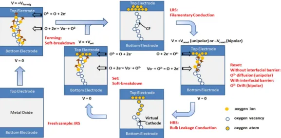
Resistive Random Access Memory (RRAM or ReRAM) is a type of memory consisting of a Metal-Insulator-Metal (MIM) structure wherein a thin metal oxide layer is sandwiched between two metal electrodes as depicted in Figure 1.2.2 (Bottom left). The basic principle of RRAMs relies on the formation and dissolution of a Conductive Filament (CF) in the oxide layer [41–43]. Initially, fresh RRAM samples are in a pristine state featuring a high resistance value. Upon the application of an initial forming voltage between the Top and Bottom Electrodes (TE and BE, respectively) during the so-called forming operation, the CF is created by soft dielectric breakdown. This process is reversible: the CF can be partially disrupted by applying a Reset voltage between the TE and BE during a Reset operation, and it can be formed again by applying a Set voltage during a Set operation. Forming the CF shunts the TE and BE and results in a drop of the RRAM electrical resistance - this leads to the Low Resistance State (LRS) -, whereas disrupting the CF disconnects the two electrodes and prevents current conduction in the oxide layer - this leads to the High Resistance State (HRS). Note that RRAMs in the HRS feature a lower resistance value than their pristine resistance value since the CF is only partially disrupted [41, 43–46]. For memory applications, the LRS and HRS are used to store one bit of information: the LRS is associated to a binary ’1’ and the HRS to a binary ’0’. Switching back and forth between the LRS and HRS is called a switching cycle and can be repeated as many times as permitted by the RRAM technology [47–49]. The maximum number of switching cycles permitted by a technology defines its programming endurance - sometimes also termed cycling endurance or just
endurance. Depending on their switching mode, RRAMs can be distinguished
between unipolar devices wherein Set and Reset operations are performed with the same polarity - i.e. voltage biases are applied on the same electrode for both operations - or bipolar devices wherein Set and Reset polarities must be alternated. If the unipolar switching can symmetrically occur on both electrodes, it is also referred to as a nonpolar switching mode [44]. The switching mode depends on the choice of oxide layer and electrode materials [42, 50]. In some cases, both unipolar and bipolar switching modes can be observed in the same device [51]. Unipolar devices allow for reduced design complexity since both operations are performed with the same polarities. However, they typically require higher programming currents with respect to bipolar devices [46]. RRAM devices can be classified into (i) Oxide-based RAM (OxRAM) and (ii) Conductive-Bridge RAM (CBRAM). In OxRAM technology, the CF is composed of oxygen vacancies in the oxide layer [52]. In CBRAM technology, the CF is attributed to the migration of metallic cations, such as copper and silver [53]. OxRAM generally presents low resistance ratios between its HRS and LRS (≈10-100) but good programming endurance (>1012 cycling operations),
whereas CBRAM features higher resistance ratios (103-106) but lower endurance
(<104) [44, 46, 54, 55]. In this work, we will only focus on bipolar OxRAM
are HfOx, AlOx, TiOx, and TaOx [44]. Figure 1.2.2 illustrates the switching
process in an OxRAM device. During the forming operation, oxygen atoms in the oxide layer drift towards the top electrode due to the application of a high electric field. This generates defects in the oxide layer and leads to the creation of a CF made of oxygen vacancies. The interface between the top electrode and the oxide layer acts like an oxygen reservoir [42, 44]. During Reset operations, the CF is disrupted by recombination of oxygen vacancies and oxygen atoms. Set operations reform the CF by pushing oxygen atoms back to the top electrode. Over the last decade, RRAMs have been seen as a promising candidate to replace Flash memories. Aside from their non-volatility property, RRAMs present numerous advantages, such as good programming endurance (>1012
[56, 57]), non-destructive read operations, fast switching (below nanoseconds [58–60]), and low-current programming operations thanks to the filament nature of current conduction (tens of nanoamperes [61–65]). As the width of the CF can be smaller than 10 nm [52], RRAMs can potentially be scaled down below 10-nm dimensions [66]. Despite all its advantages, RRAM still faces two major roadblocks that have prevented it so far from being integrated in large arrays. First, the initial forming voltage (2-3V) is significantly higher than the operating voltage. Second, RRAM is strongly affected by extrinsic and intrinsic resistance variability arising from the fabrication process as well as the intrinsic stochastic nature of the CF formation. These challenges are discussed more in details in the next section.
Figure 1.2.2: Schematic illustration of the switching process in Oxide-based Resistive Memories (OxRAMs). An initial forming process generates oxygen vacancies in the oxide layer by soft dielectric breakdown. Subse-quent Set and Reset operations lead to the formation and dissolution of a Conductive Filament (CF) made of oxygen vacancies, respectively. The interface between the oxide layer and the top electrode acts like an oxygen reservoir. Reproduced from [44].
Phase-Change Random Access Memory
Phase-Change Random Access Memory (PCM or PCRAM) is composed of two electrodes sandwiching a chalcogenide glass that can change between a crystalline and an amorphous phase. The most used chalcogenide material in PCM is the ternary compound Ge2Sb2Te5, also referred to as GST [67–70]. As for RRAM,
PCM stores one bit of information by modulating its electrical resistance. The resistance modulation relies on the transition between the crystalline and the amorphous phase of the chalcogenide material. The crystalline state features a low electrical resistance - corresponding to the Low Resistance State, LRS - while the amorphous state features a high electrical resistance - the High Resistance State, HRS. This transition occurs by passing a current through the material to heat it up by Joule heating. The advantage of PCM is that the ratio between the HRS and LRS resistance values is generally larger than that of RRAM technology, thus making it promising for multi-bits storage and facilitating its integration into large arrays. However, PCM technology suffers from resistance
drift over time towards higher resistance values, in particular in the amorphous
phase - i.e. mainly in the HRS [71]. This makes it difficult to distinguish the programmed states over time. Another drawback of PCM technology is its high current consumption during programming, especially during Reset operations. Since PCM is programmed by Joule heating, the programming current scales down with device area. Yet even for PCM devices scaled down to sizes smaller than 10 nm, programming current of the order of microamperes is still required [72, 73].
Spin-Transfer-Torque Magnetic Random Access Memory
Spin-Transfer-Torque Magnetic Random Access Memory (STT-MRAM) is a type of magnetic memory based on the most advanced currently available technology to achieve higher scalability. STT-MRAM stores the information (i.e. ’0’ or ’1’) in the magnetisation of ferromagnetic materials. It is composed of two ferromagnetic layers separated by a thin insulator layer. The basic principle of STT-MRAM relies on the switching of magnetisation of one ferromagnetic layer (the free layer), while the magnetisation of the other layer is fixed (the pinned layer) [9]. If the free layer has the same magnetisation as the pinned layer - the parallel configuration -, electrons have a higher probability to pass through the device. This corresponds to the LRS. Conversely, if the free layer has an opposite magnetisation - the anti-parallel configuration -, the device is in the HRS since the anti-parallel configuration prevents current conduction. STT-MRAM provides numerous advantages, such as low-energy programming, high speed, and almost unlimited programming endurance [12]. In addition, it shows high uniformity in its resistance states, unlike RRAM technology. However, one of the main drawbacks of STT-MRAM technology is its low resistance ratio between the LRS and the HRS. This requires the use of specific memory cell architecture to mitigate the low resistance ratio that limits STT-MRAM scalability [9, 12, 74].
Comparison of the main metrics and summary
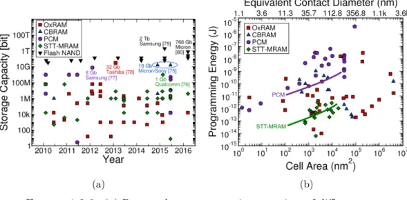
Several prototypes of RRAM [78, 81], PCM [77], and STT-MRAM [76] have been demonstrated, up to several gigabits as reported in Figure 1.2.3 (a). Commercial products are already available by different companies, such as Intel and Micron with the 3D XPoint technology [82], Panasonic [83], Avalanche [84], or Everspin [85]. Figure 1.2.3 (b) compares reported programming energy as a function of cell area. Unlike PCM and STT-MRAM, programming energy of RRAM technology (encompassing OxRAM and CBRAM) does not scale
(a) (b)
Figure 1.2.3: (a) Reported storage capacity over time of different non-volatile memory technologies. Multi-gigabits prototypes with the new non-volatile memories have been reported [75–78]. Data on Flash NAND technology are reported for comparison [79, 80]. (b) Programming energy as a function of cell area. Programming energy of Resistive Memories (RRAMs, encompassing OxRAM and CBRAM technologies) does not depend on cell area due to the filament conduction nature of RRAMs. Reproduced from [54].
with cell area due to the filament conduction nature of RRAMs. A significant advantage of these new non-volatile memories is that they can be monolithically integrated in three-dimension with CMOS logic circuits because their fabrication temperature is compatible with the back-end-of-line, and they aare fabricated with materials commonly used in the semiconductor industry. This facilitates the implementation of in-memory computing architectures by physically bringing memory units close to processing cores and can improve computing efficiency by many orders of magnitude [12, 19]. In addition, each of these devices can be independently programmed bit by bit, whereas Flash memories require to erase whole blocks of kilobits whenever any individual bit in the array needs to be reprogrammed. Finally, they are two-terminals devices, unlike conventional three-terminals CMOS-based DRAMs or Flash memories, and can be integrated into so-called crossbar arrays in between densely packed word lines and bit lines. This allows for an extremely small bit area of only 4F2/n, where F is the minimal
lithographic feature size and n the number of stacked layers [46].
1.2.1.3 Challenges of resistive memory technology
This part provides more details about the main metrics and challenges with RRAMs that will be discussed in this work, namely the memory window, the programming endurance, and the resistance variability.
In RRAM technology - encompassing OxRAM and CBRAM technologies - the resistance values of LRS and HRS depend on the programming conditions, i.e. the applied voltage, programming time, and programming current - related to the
failures due to the abrupt increase of current during forming and Set operations. It can be defined by programming equipment or in practice by integrating in series a selector element, such as a diode or a transistor [43, 78, 86, 87]. It has been demonstrated that programming time exponentially depends on programming voltage [88–90]. Therefore, programming time is usually fixed and only the programming voltage varies. LRS resistance values are mostly defined by Icc during the Set operation [46]. One of the universal characteristics
of RRAM is that LRS resistance values have a power law dependency on Icc as
shown in Figure 1.2.4 (a): increasing Icc results in lower LRS resistance values,
RLRS. On the other hand, HRS resistance values are mainly defined by Reset
programming voltages [91], and using higher voltages during Reset operations leads to higher HRS resistance values, RHRS(cf Figure 1.2.4 (b)). This provides
important guidelines for programming RRAM devices. As explained previously, RRAM stores one bit of information in its LRS and HRS, thus it is fundamental to guarantee a sufficient ratio between both states, RHRS/RLRS, in order to
discriminate them. Ideally, the ratio RHRS/RLRS, often called the Memory
Window (MW), has to be maximised in order to facilitate the integration of
RRAMs into large arrays. However, it has been demonstrated that a trade-off exists between the MW and programming endurance performance: higher MWs imply lower programming endurance [49, 54, 55, 90]. Figure 1.2.5 shows two typical RRAM endurance characterisations performed on a GeS2/Ag (a) and a
HfO2/GeS2/Ag (b) RRAM stack, i.e. the evolution of LRS and HRS resistance
values after different numbers of Set/Reset switching cycles [90]. During the cycling, HRS resistance values generally tend to decrease, and some cells can be permanently stuck in the LRS after a certain number of switching cycles [43, 44, 48, 92]. This results in a decrease of the MW. We define here the
programming endurance as the maximum number of Set/Reset cycles we can
perform with a stable MW. While it is possible to sustain a low constant MW of about 10 during 108 cycles (Figure 1.2.5 (a)), only 103 cycles can be performed
with a large MW of 106 (Figure 1.2.5 (b)). Figure 1.2.5 (c) reports the
memory window of different RRAM technologies associated to the corresponding endurance. For the sake of comparison, some data on PCM and STT-MRAM technologies are also reported. As it can observed, endurance performance higher than 106 cycles for RRAM to be comparable to Flash technology [12, 93]
-is usually associated to low memory windows below 10-100. Th-is low MW -is critical for large memory arrays due to sneak paths issues [86]. Therefore, selector devices have to be integrated in series with each RRAM device to limit leakage currents - usually a CMOS transistor in the so-called one-transistor/one-RRAM (1T1R) structure. However, this limits storage density [94].
Another main drawback of RRAM technology is its high resistance variability -both across cycles and devices - inducing non-repeatable behaviours [43, 95, 96]. As it is illustrated in the endurance characterisations in Figure 1.2.5, LRS and HRS resistance values vary at every switching cycle - referred to as
cycle-to-cycle variability. Cycle-to-cycle variability can be attributed to the stochastic
nature of the conductive filament formation and dissolution. On the other hand, resistance variability also occurs across devices in a memory array -
device-to-device variability - arising from external factors like fabrication process [97].
(a) (b)
Figure 1.2.4: Low Resistance State (LRS) resistance value of different Resistive Memory (RRAM) technologies as a function of compliance current, Icc, during a Set operation. A power law relationship exists
between LRS resistance values and Icc. Reproduced from [46]. (b) High
Resistance State (HRS) resistance value as a function of the voltage applied during Reset operations, Vreset. Measurements have been performed on a
TiN/HfO2/Ti/TiN RRAM device. The mean HRS resistance value over
1000 Reset operations is shown (solid line) as well as the spread at two standard deviations (shaded area). Reproduced from [91].
TiN/HfO2/Ti/TiN RRAM array [43]. While it is possible to reach a ratio of
2500 between the median HRS and LRS resistance values, the device-to-device resistance variability - mainly in the HRS [43, 44] - degrades this ratio down to 600 if one considers the ratio between HRS and LRS resistance values at -3σ and +3σ, respectively. Numerous works have tried to tackle and mitigate resistance variability, for instance by material and process engineering [98, 99]. Understanding better the physics of RRAM is still an active area.
A last issue that can be mentioned is the need of an initial forming operation [98]. In order to generate a sufficient amount of defects to initiate the switching [44], high forming voltages (≈2-3 V) associated with a high electric field (>10 MV/cm) are required [44, 54]. This is higher than the power supply voltage and any subsequent programming operations, and it is not desirable for practical applications. In addition, it constraints the transistor used as a selector in order to prevent any degradation at such a high voltage [13]. Therefore, there have been significant efforts in the literature to design forming-free RRAM devices [64, 100–102]. For instance, it has been found that the forming voltage is linearly dependent on the thickness of the oxide layer, and HfOx-based RRAMs can be
free of the forming operation below 3 nm [100]. However, it may severely decrease HRS resistance values and the memory window. It has also been reported that forming voltages can be reduced by engineering around the fabrication process [44].
To summarise, main challenges of RRAM technology are:
• the low memory window (<10-100) in order to ensure sufficient program-ming endurance (>106 cycles)
• the high cycle-to-cycle and device-to-device resistance variability that limits the memory window
(a) (b)
(c)
Figure 1.2.5: Typical endurance characterisations performed on (a) a GeS2/Ag and (b) a HfO2/GeS2/Ag Resistive Memory (RRAM) stack.
While it is possible to sustain a low resistance ratio Roff/Ron of 10 during
108 switching cycles, only 103 switching cycles can be performed with
a large resistance ratio of 106. Reproduced from [90]. (c) Reported
Memory Window (MW) as a function of programming endurance for different RRAM technologies. Data on Phase-Change Memory (PCM) and Spin-Torque-Transfer Magnetic Memory (STT-MRAM) are reported for comparison. A general trend of lower MWs with higher endurance performance is observed. Reproduced from [54].
Figure 1.2.6: High Resistance State (HRS, red) and Low Resis-tance State (LRS, black) resisResis-tance distributions measured on a 4-kbit TiN/HfO2/Ti/TiN Resistive Memory (RRAM) array, after one Reset/Set
cycle, respectively. While a resistance ratio of 2500 is measured between the median HRS and LRS resistance values, it is reduced to 600 at three standard deviations, 3σ, due to device-to-device resistance variability. Reproduced from [43].
1.2.2 Three-dimensional technology
Another technological solution to continue Moore’s law trends is to benefit from the third dimension, i.e. the vertical axis. Three-dimensional (3D) integration allows to pack more components on a given silicon area. We first provide an overview of 3D integration with Resistive Memories (RRAMs, presented in Section 1.2.1), then 3D integration with Complementary Metal-Oxide-Semiconductor (CMOS) technology.
1.2.2.1 Three-dimensional integration of resistive memories
Figure 1.2.7: Transmission electron microscopy of a TiN/HfO2/Ti/TiN
RRAM fabricated on top of a NMOS transistor. RRAMs have been integrated in the back-end-of-line. Reproduced from [103].
Two main concepts were proposed with Resistive Memories (RRAMs) in order to benefit from the third dimension. They take advantage of RRAM Back-End-Of-Line (BEOL) CMOS process compatibility and the simple Metal-Insulator-Metal (MIM) structure of RRAM. The first concept consists in stacking one or several layers of RRAM devices directly on top of CMOS logic circuits in the BEOL [19, 104]. For instance, RRAMs can be fabricated on top of NMOS or PMOS transistor contacts in the so-called one-transistor/one-RRAM (1T1R) structure as shown in Figure 1.2.7. Another case in point are
cross-point architectures with RRAMs [105, 106] wherein memory cells are located in between densely stacked word lines and bit lines (cf Figure 1.2.8(a)), such as the 3D XPoint technology of Intel and Micron [82]. This design allows to use every word- and bit-line for two consecutive layers of memory devices, thus halving the number of metal layers. The second possible 3D integration concept is called Vertical RRAM (VRRAM) wherein MIM layers are integrated vertically in a pillar (cf Figure 1.2.8 (b)) [61, 62, 107–110]. The pillar is a common vertical electrode (the metal (M), e.g. TiN/Ti) whose sidewall is covered by the resistive switching layer oxide (the insulator (I), e.g. HfOx). Horizontal metal
layers are stacked on top of each other and form the other electrode (the metal (M), e.g. TiN). Memory elements are located where the horizontal electrode
(a) (b)
Figure 1.2.8: (a) Schematic drawing of a three-dimensional (3D) cross-point Resistive Memory (RRAM) structure. RRAM cells are located in between densely stacked word-lines and bit-lines. Reproduced from [109]. (b) (Left) Schematic drawing of Vertical RRAM (VRRAM) arrays (reproduced from [109]), and (Right) transmission electron microscopy of
a four-layers TiN/Ti/HfOx/TiN VRRAM (reproduced from [110]).
1.2.2.2 Three-dimensional integration of CMOS transistors
Although RRAMs can easily be fabricated on top of CMOS transistors thanks to their low-temperature process, stacking several layers of CMOS transistors on top of each other poses more challenges. Two 3D integration types can be distinguished: (i) the parallel integration, and (ii) the sequential integration as depicted in Figure 1.2.9. In the parallel integration - sometimes called
3D packaging (Figure 1.2.9 (a)) - the different layers (tiers) of transistors
are processed separately, then vertically stacked and connected afterward (for instance with Through-Silicon Via (TSV) or Through-Oxise Via (TOV)). In the sequential integration also termed monolithic integration (Figure 1.2.9 (b)) -every tier of transistors is fabricated directly on top of the previous one. The parallel integration has the advantage of much simpler manufacturing process with respect to the sequential integration, yet it suffers from lower alignment accuracy since it requires to align two whole tiers together (see Figure 1.2.9 (c)). On the other hand, in the sequential integration, a tier is fabricated directly on top of the previous one. Therefore, it can reach alignment accuracy at the transistor scale as it only depends on lithographic alignment on the stepper. This is a significant advantage of monolithic integration over parallel integration as it allows to improve interconnection density by a factor 50x (1010vias/cm2 vs 2.108
vias/cm2, respectively) [113]. Yet the major downside of monolithic integration
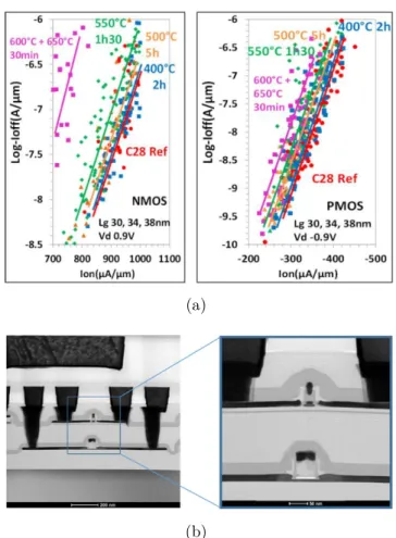
is its fabrication process: the fabrication of a tier can degrade performance of lower tiers if process temperature is not kept low enough [111, 113, 114]. For instance, it has been demonstrated that transistors fabricated in a 28-nm Silicon On Insulator (SOI) process can sustain thermal budget up to 500°C for 5 hours without noticeable performance degradation (cf Figure 1.2.10 (a)) [115]. At higher thermal budget (i.e. temperature and process time), degradation comes from silicide deterioration of CMOS transistors as well as from a slight dopant deactivation [115]. However, standard thermal budget to manufacture a transistor is usually higher than 1000°C [112]. As a result, it is mandatory to either improve transistor thermal stability and/or adapt manufacturing process to enable low-temperature transistor fabrication, while
(a) (b)
(c)
Figure 1.2.9: Schematic illustrations of three-dimensional (3D) (a) par-allel integration, and (b) sequential integration. In the parpar-allel integration both layers are fabricated separately, then vertically stacked and connected. In the sequential integration the top layer is fabricated directly on top of the bottom layer. Reproduced from [111]. (c) Alignment accuracy as a function of 3D contact width. 3D sequential integration allows for higher alignment accuracy than parallel integration since it only depends on lithographic alignment on the stepper. Reproduced from [112].
sustaining high transistor performance for every tier [116]. Different research groups [117–121] have proposed solutions to overcome these problems, however they generally require complex and expensive fabrication process [119, 120], for instance with the use of III-V materials, or result in lower electrical performance of top tiers [117, 118, 121]. CoolCube™technology [112] developed by CEA-Leti is an example of 3D monolithic integration of SOI CMOS transistors. Currently, it allows for monolithic integration of two tiers of CMOS transistors in a 65-nm SOI process without noticeable degradation of electrical performance. In addition, it is fabricated with conventional foundry process. Therefore, it is compatible with industrial requirements, in particular with hard contamination constraints. A first layer of CMOS transistors is fabricated in a conventional SOI 65-nm design rules CMOS over CMOS process (the bottom tier). Then, the active area of the next layer (the top tier) is obtained by transferring a new SOI substrate on top of the bottom tier by oxide bonding. Finally, top tier transistors are fabricated directly on the new top active area with alignment accuracy at the transistor scale as shown in the transmission electron microscopy in Figure 1.2.10 (b). Chapter 4 will describe more in details the fabrication process of CoolCube™technology. Preliminary studies have evaluated potential benefits of CoolCube™integration, for instance on a 3D Field-Programmable Gate Array (FPGA) architecture in [122]. In the 3D FPGA architecture, memory components are placed on the bottom tier and logic circuits on the top tier in order to keep a good global performance. Compared to a planar FPGA architecture, the 3D FPGA architecture can reduce area consumption by 55% and the energy-delay product by 47%. In terms of cost benefits, a cost model developed in [123] has predicted benefits of the order of 50% with 300-mm2
(12-inch) wafers.
1.2.2.3 Motivations of this work
The first advantage of 3D integration is the possibility to pack more components on a given silicon area, thus increasing component density. In particular, 3D monolithic integration could virtually grant access to a new technology node by stacking two tiers fabricated at a previous CMOS technology node, while being potentially more economically advantageous than developing a new technology node [111, 123]. Another advantage of such integration is that interconnections are in average shorter than those of for a planar integration. This results in less parasitic capacitance as well as less routing congestion [111, 112, 122, 124]. Also, 3D integration can facilitate heterogenous integration [119–121]. N3XT [19] is an example of computing systems implementing many novel technologies, such as RRAM, STT-MRAM, and carbon nanotubes, integrated in a 3D monolithic technology. Such systems are expected to provide significant gains in performance - up to 1000x in energy-delay product. Another case in point is the gas sensor chip fabricated and tested in [104] wherein four layers have been monolithically fabricated - one layer of silicon FET logic circuits, two layers of carbon nanotubes, and one layer of RRAM.
In this thesis, we propose the 3D monolithic integration of several layers of
high-performance CMOS transistors with Resistive Memories (RRAMs). To this
(a)
(b)
Figure 1.2.10: (a) (Left) NMOS and (Right) PMOS Ioff/Ion
perfor-mance for different thermal annealings. Transistor perforperfor-mance can be ensured for annealing up to 500°C for 5 hours. Reproduced from [115]. (b) Transmission electron microscopy of two tiers of NMOS transistors fabri-cated in a 3D monolithic 65-nm SOI process with CoolCube™technology. Reproduced from [112].
transistors using CoolCube™technology of CEA-Leti [112] with an additional tier of RRAMs fabricated directed on top of the two tiers of CMOS transistors in the BEOL. Chapter 4 will describe the fabrication process of RRAMs with CoolCube™CMOS transistors and show the electrical functionality of the integration.
1.3 The third generation of neural networks:
Spiking neural network
This section presents an overview of Spiking Neural Network (SNN) systems and the main building blocks of hardware SNNs.
1.3.1 Overview of spiking neural networks
1.3.1.1 Biological brains
It is now known that brains are much more efficient at computing than con-ventional computers based on the Von Neumann architecture. The human brain computes with a meagre power budget of 10-20 W ([125, Section 5.8.2]), improving on Von Neumann computers by millions of fold in terms of power efficiency [126–130]. It is an extremely complex computational engine consisting of 1011 computing elements, the neurons, densely interconnected by more than
1014 connections, the synapses [131]. Although most of neural computation is
still to be understood, it is widely accepted that memory is stored in synapses, while computation takes place in neurons [132–135]. Neurons are cellular units specialised for the processing of cellular signals. They are mainly composed of a soma, several dendrites, and an axon as shown in Figure 1.3.1, and they communicate between each other via electrical signal events, the Action
Poten-tials (APs), transmitted along synapses [136]. APs are sharp electrical pulses of
about 100 mV and 1 ms. Input APs coming from other neurons are received by the dendrites and integrated inside the soma. At rest, the membrane potential of neurons - i.e. the difference in electric potential between the inside and outside of neurons - is typically in the range of -40 to -90 mV. Upon integrating APs, the membrane potential fluctuates. If it goes below the resting membrane potential, nothing really happens. If it goes above the resting potential and reaches the threshold potential level, the neuron fires an AP from its axon to other neurons it is connected to. Axon terminals connect to other neuron dendrites through terminal buttons forming synapses. Pre- and post-synaptic terminals are physically separated by a synaptic cleft whose length is in the order of 20 nm. Two types of synapses can be distinguished: (i) chemical synapses, and (ii) electrical synapses. In chemical synapses, the most abundant type of synapses, synaptic transmissions are carried out by release of neurotransmitters stored in synaptic vesicles that bind to receptors at the postsynaptic terminal. In electrical synapses, ions can directly diffuse between pre- and post-synaptic terminals.
Brain efficiency can be accounted for by several factors. First, brains are mas-sively parallel computing systems: all synapses and neurons can transmit and process information in parallel. Second, they use short and low-voltage pulses at low operating frequencies (10-100 Hz) for communication [68, 130] result-ing in high resource-efficiency [137, 138]. Finally, another factor of efficiency may lie in the vast heterogeneity and diversification of brain circuit elements [131]. Synapses and neurons continuously adapt over time via learning [135]. In particular, the strength of each synapse, the synaptic weight, can be tuned to facilitate or prevent the transmission of APs. During learning, synaptic weights are constantly adjusted to respond to specific cognitive tasks.
1.3.1.2 The different generations of neural networks
Three different generations of neural networks can be distinguished. The first generation is based on the seminal works of Rosenblatt [139] on the perceptron.
Figure 1.3.1: Drawing of two connected neurons. A neuron is mainly composed of a soma, several dendrites, and an axon. Neurons transmit electrical signal events (action potentials) along their axon connected to other neuron dendrites. Axon terminals connect to other neuron dendrites through terminal buttons forming synapses.
Perceptrons are based on McCulloch-Pitts neurons [2] and act as all-or-none elements. They output a boolean value depending on if their inputs reach a certain threshold value or not. The second generation is based on so-called
Artificial Neural Networks (ANNs). ANNs are composed of a collection of
computing units, the artificial neurons, interconnected by weighted synapses. Unlike perceptrons, artificial neurons can provide a continuous set of possible output values by applying an activation function to the weighted sum of their inputs. This second generation of neural networks have provided solutions to many artificial intelligence applications, such as pattern recognition, natural language processing, forecasting and prediction, or speech recognition [12, 15, 140, 141]. As illustrations of the success of ANNs we can cite the facial recognition system DeepFace by Facebook [142] and AlphaGo by Google DeepMind [126] that defeated one of the best human professional players in the full-size game of Go, something that was thought not to be possible before at least another decade. More recently, Google DeepMind introduced their program AlphaStar that reached the rank of Grandmaster at the real-time strategy game StarCraft II - the highest league above 99.8% of officially ranked human players [128]. This is highly promising for applications requiring real-time decisions, such as self-driving cars or robotics.
Although ANNs have been introduced to provide more bio-plausible neural networks with respect to perceptrons, they eventually deviated from biology to
focus on performance instead of power efficiency [143, 144]. For instance, training AlphaStar [128] required the use of 384 third-generation Tensor Processing Units for 44 days. By contrast, Spiking Neural Networks (SNNs) aim to reproduce biological brains in a closer manner with the promise of achieving high energy-efficiency systems [16, 145–150]. This gives rise to the third generation of neural networks [151]. As in biological brains, SNNs mainly rely on the exchange of spikes between neurons - the action potentials - that are transmitted along weighted synapses. Information is encoded in the timing and spiking rate of spikes [152–155]. For neuronal processing, SNNs employ spiking neurons, also called integrate-and-fire neurons (IF neurons) [148, 156]. IF neurons sum input spikes - integrate - whose amplitudes are modulated by synaptic weights, and they emit a spike - fire - when the summation goes above a threshold level. In the scope of this PhD thesis, we will focus on SNNs. The rest of this section will present the main building blocks of hardware SNN systems.
1.3.2 Information coding and network routing
1.3.2.1 The address event representation communication protocol
In Spiking Neural Networks (SNNs) neurons communicate using spikes. The information can be encoded in the time of occurrence of spikes, time difference between consecutive spikes, or spiking rates [152–155]. From an hardware implementation point of view, the Address Event Representation (AER) [157, 158] has been proposed as an efficient communication protocol for SNNs based on time-multiplexing. A ”brute force” approach to transmit spikes between neurons would be to use one wire for each pair of neurons, i.e. N wires for N pairs of neurons [159]. In the AER protocol each neuron is assigned an address that is encoded as a digital word. When a neuron fires a spike, also called an
event, its address is sent across a shared data bus to a receiver circuit using
asynchronous digital circuits [22, 129, 130, 145, 147, 160–162]. The receiver decodes the address and transmits an event to every neuron paired with the spiking neuron. The AER allows to reduce the number of wires from N to ≈log2(N) [159]. Note that a handshake protocol is required to ensure that only
one address is transmitted in the shared digital bus at a time. Therefore, it is crucial that all events can be processed and transmitted quick enough to prevent routing congestion [163, 164].
1.3.2.2 Impact of network topology
In biological brains part of neural computation lies in the network topology,
i.e. the connectivity scheme between neurons (the connectome) [165–167]. For
instance, neurons have the ability to extend their neurites, i.e. dendrites and axons, to find appropriate synaptic partners [136]. The growth of neurites is not random, and neurites seek for particular targets on a basis of trials-and-errors [168]. Another example is the synaptic pruning process that mainly occurs in the early childhood and puberty [169]. Synaptic pruning consists in the elimination of synapses and may be an energy-saving process wherein redundant
synapses are eliminated. For neuromorphic systems, it has been shown that the choice of network topology affects network outcomes, performance, and energy [170–173]. Therefore, it is crucial that neuromorphic processors are not bound to a fixed topology and can adapt their synaptic connections to a specific task [163, 164]. The use of synaptic Lookup Tables (LUTs) associated with the AER protocol is an efficient method to enable network topology reconfigurability [129, 145, 159, 161, 163]. Synaptic LUTs store the addresses of pre-synaptic neurons, and they map them with the addresses of paired post-synaptic neurons. When a neuron spikes, its address is searched inside the synaptic LUTs. This allows to retrieve the addresses of post-synaptic neuron it is virtually connected to. As a result, the network topology can be modified by simply reprogramming synaptic LUTs. However, routing congestion can appear if the time to process an event, in particular the time to search an address in the LUTs, is longer than the time between two consecutive events.
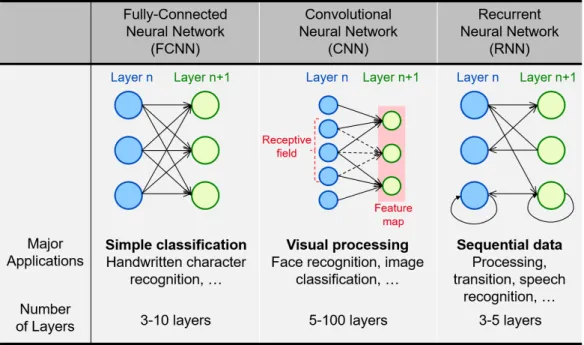
Figure 1.3.2 shows the three main neural network architectures: (i) Fully-Connected Neural Network (FCNN), (ii) Convolutional Neural Network (CNN), and (iii) Recurrent Neural Network (RNN). FCNN is the simplest topology wherein every neuron of a layer is connected to every neuron of the next layer. It is mainly used for tasks such as classification or detection [174, 175]. CNNs are designed to process data that come in the form of multiple arrays, for example a colour image composed of three two-dimensional arrays containing pixel intensities in the three colour channels [15]. Neurons in a convolutional layer are organised in feature maps wherein each neuron is connected to a small subset of neurons, receptive field, of the previous layer [176]. Convolutional layers require fewer synapses than fully-connected layers, and they have the advantage to be insensitive to the spatial location of specific features in the inputs. For instance, if a CNN is sensitive to specific motifs from input images, it can detect them whatever their spatial location in the inputs. CNNs are mainly used for visual processing like face recognition and have achieved so far the highest performance in image classification [177]. The third main architecture is the RNN wherein feedback loops are included inside the network topology. This allows to store an input information, while processing new inputs. For this reason, RNNs are often used in tasks that involve sequential inputs, such as speech and language recognition.
Chapter 3 focuses on the implementation of synaptic LUTs for SNNs, and more details are provided in this chapter.
1.3.3 Hardware spiking neuron: the leaky
integrate-and-fire neuron model
A canonical neuron model used in SNNs is the Leaky Integrate-and-Fire (LIF) neuron [156]. As biological neurons, LIF neurons rely on the integration of synaptic input currents and fire a spike when the integration value reaches a certain threshold [178, 179]. From a system point of view, LIF neurons receive input currents from excitatory or inhibitory synapses. If the synapse is excitatory, the current is positive. Otherwise, it is negative. The stronger a synapse, i.e. the higher its synaptic weight, the higher the current absolute value. These
Figure 1.3.2: The three main neural network architectures: Fully-Connected Neural Network (FCNN), Convolutional Neural Network (CNN), and Recurrent Neural Network (RNN). Adapted from [12].
input currents are then integrated by LIF neurons. That is, LIF neurons can be modelled by an internal state variable, X, that evolves according to a first-order differential equation [16]:
τleakdX
dt + X = Iinput (1.3.1)
wherein X represents the integrated current value, τleak is an integration time
constant, and Iinput is the input synaptic current. Upon receiving input synaptic
currents, X increases (or decreases if the synapse is inhibitory). Between two integrations, X exponentially decreases with a time constant τleak. When X
reaches a certain current threshold value, Ith, the neuron emits a spike, and X is
reset to zero. After emitting a spike, LIF neurons are unable to integrate any input synaptic current for a refractory period. Lateral inhibition can also be implemented: when a LIF neuron spikes, it also inhibits neighbouring neurons from integrating input currents for a certain duration tinhib. This allows to
implement winner-take-all systems to prevents different neurons from being selective to similar features [174, 180].
Figure 1.3.3 (a) shows a simple LIF neuron circuit originally proposed in [181]. The capacitance Cmem, referred to as the membrane capacitance, models
the membrane of a biological neuron [148]. Figure 1.3.3 (b) illustrates the evolution of the membrane capacitance potential, Vmem, during the generation
of an action potential. Upon being fed by excitatory input currents, Iin, Cmem
charges up (integration). Respectively, inhibitory currents (not shown) remove charges from Cmem. In the absence of input currents, Cmem discharges to its
resting potential (ground in this case) through leakage currents controlled by
the gate voltage Vlk and a time constant τleak dependent on Cmem value. Vmem is
compared to a threshold voltage, Vthr, using a basic transconductance amplifier
![Figure 1.3.3: (a) Example of a bio-inspired silicon-based Leaky Integrate- Integrate-and-Fire (LIF) neuron circuit from [181]](https://thumb-eu.123doks.com/thumbv2/123doknet/12716583.356476/37.892.250.673.130.701/figure-example-inspired-silicon-leaky-integrate-integrate-circuit.webp)
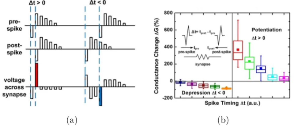
![Figure 1.3.4: Experimental Spike-Timing Dependent Plasticity (STDP) observed by Bi and Poo [133]](https://thumb-eu.123doks.com/thumbv2/123doknet/12716583.356476/39.892.284.640.130.441/figure-experimental-spike-timing-dependent-plasticity-stdp-observed.webp)
![Table 1.1: Summary of reported silicon-proven multi-core spiking neuro- neuro-morphic processors [22, 129, 130, 145, 161, 162].](https://thumb-eu.123doks.com/thumbv2/123doknet/12716583.356476/44.892.140.721.454.698/table-summary-reported-silicon-proven-spiking-morphic-processors.webp)