HAL Id: hal-02011567
https://hal.univ-lorraine.fr/hal-02011567
Submitted on 8 Feb 2019HAL is a multi-disciplinary open access archive for the deposit and dissemination of sci-entific research documents, whether they are pub-lished or not. The documents may come from teaching and research institutions in France or abroad, or from public or private research centers.
L’archive ouverte pluridisciplinaire HAL, est destinée au dépôt et à la diffusion de documents scientifiques de niveau recherche, publiés ou non, émanant des établissements d’enseignement et de recherche français ou étrangers, des laboratoires publics ou privés.
The 2017 Magnetism Roadmap
D Sander, S Valenzuela, D. Makarov, C Marrows, E. Fullerton, P. Fischer, J.
Mccord, P. Vavassori, S. Mangin, P. Pirro, et al.
To cite this version:
D Sander, S Valenzuela, D. Makarov, C Marrows, E. Fullerton, et al.. The 2017 Magnetism Roadmap. Journal of Physics D: Applied Physics, IOP Publishing, 2017, 50 (36), pp.363001. �10.1088/1361-6463/aa81a1�. �hal-02011567�
Journal of Physics D: Applied Physics
TOPICAL REVIEW • OPEN ACCESS
The 2017 Magnetism Roadmap
To cite this article: D Sander et al 2017 J. Phys. D: Appl. Phys. 50 363001
View the article online for updates and enhancements.
Related content
Magnetism in curved geometries
Robert Streubel, Peter Fischer, Florian Kronast et al.
-The 2014 Magnetism Roadmap
Robert L Stamps, Stephan Breitkreutz, Johan Åkerman et al.
-Materials and devices for all-optical helicity-dependent switching
Mohammed Salah El Hadri, Michel Hehn, Grégory Malinowski et al.
-Journal of Physics D: Applied Physics D Sander et al Printed in the UK 363001 JPAPBE © 2017 IOP Publishing Ltd 50
J. Phys. D: Appl. Phys.
JPD
10.1088/1361-6463/aa81a1
36
Journal of Physics D: Applied Physics
The 2017 Magnetism Roadmap
D Sander1, S O Valenzuela2,3 , D Makarov4, C H Marrows5 ,
E E Fullerton6 , P Fischer7,8, J McCord9, P Vavassori10,11 , S Mangin12, P Pirro13, B Hillebrands13, A D Kent14, T Jungwirth15,16 , O Gutfleisch17 , C G Kim18 and A Berger10
1 Max Planck Institute of Microstructure Physics, Halle, Germany
2 ICN2 Catalan Institute of Nanoscience and Nanotechnology, CSIC and The Barcelona Institute
of Science and Technology (BIST), Campus UAB, Bellaterra, 08193 Barcelona, Spain
3 ICREA Institució Catalana de Recerca i Estudis Avançats, 08070 Barcelona, Spain
4 Helmholtz-Zentrum Dresden-Rossendorf e.V., Institute of Ion Beam Physics and Materials Research,
Bautzner Landstrasse 400, 01328 Dresden, Germany
5 School of Physics and Astronomy, University of Leeds, Leeds LS2 9JT, United Kingdom 6 Center for Memory and Recording Research, University of California, San Diego, La Jolla,
CA 92093-0401, United States of America
7 Materials Science Division, Lawrence Berkeley National Laboratory, Berkeley, CA 94720,
United States of America
8 Physics Department, University of California, Santa Cruz, CA 94056, United States of America 9 Kiel University, Institute for Materials Science, Kaiserstr. 2, 24143 Kiel, Germany
10 CIC nanoGUNE, E-20018 Donostia-San Sebastian, Spain
11 IKERBASQUE, The Basque Foundation for Science, E-48013 Bilbao, Spain 12 Institut Jean Lamour, UMR 7198 CNRS-Université de Lorraine, France
13 Fachbereich Physik and Landesforschungszentrum OPTIMAS, Technische Universität Kaiserslautern,
67663 Kaiserslautern, Germany
14 Department of Physics, New York University, New York 10003, United States of America 15 Institute of Physics, Czech Academy of Sciences, Czech Republic
16 University of Nottingham, Nottingham, United Kingdom 17 Material Science, TU Darmstadt, Darmstadt, Germany
18 Department of Emerging Materials Science, DGIST, Daegu, 42988, Republic of Korea
E-mail: [email protected], [email protected], [email protected], [email protected], [email protected], [email protected], [email protected], [email protected],
[email protected], [email protected], [email protected], [email protected], [email protected], [email protected], [email protected] and [email protected]
Received 10 May 2017, revised 17 July 2017 Accepted for publication 24 July 2017 Published 21 August 2017
Abstract
Building upon the success and relevance of the 2014 Magnetism Roadmap, this 2017 Magnetism Roadmap edition follows a similar general layout, even if its focus is naturally shifted, and a different group of experts and, thus, viewpoints are being collected and presented. More importantly, key developments have changed the research landscape in very relevant ways, so that a novel view onto some of the most crucial developments is warranted, and thus, this 2017 Magnetism Roadmap article is a timely endeavour. The change in landscape is hereby not exclusively scientific, but also reflects the magnetism related industrial application portfolio. Specifically, Hard Disk Drive technology, which still dominates digital storage and will
continue to do so for many years, if not decades, has now limited its footprint in the scientific
Topical Review
IOP
Original content from this work may be used under the terms of the Creative Commons Attribution 3.0 licence. Any further distribution of this work must maintain attribution to the author(s) and the title of the work, journal citation and DOI.
2017
1361-6463
https://doi.org/10.1088/1361-6463/aa81a1
and research community, whereas significantly growing interest in magnetism and magnetic materials in relation to energy applications is noticeable, and other technological fields are emerging as well. Also, more and more work is occurring in which complex topologies of magnetically ordered states are being explored, hereby aiming at a technological utilization of the very theoretical concepts that were recognised by the 2016 Nobel Prize in Physics.
Given this somewhat shifted scenario, it seemed appropriate to select topics for this Roadmap article that represent the three core pillars of magnetism, namely magnetic materials, magnetic phenomena and associated characterization techniques, as well as applications of magnetism. While many of the contributions in this Roadmap have clearly overlapping relevance in all three fields, their relative focus is mostly associated to one of the three pillars. In this way, the interconnecting roles of having suitable magnetic materials, understanding (and being able to characterize) the underlying physics of their behaviour and utilizing them for applications and devices is well illustrated, thus giving an accurate snapshot of the world of magnetism in 2017. The article consists of 14 sections, each written by an expert in the field and addressing a specific subject on two pages. Evidently, the depth at which each contribution can describe the subject matter is limited and a full review of their statuses, advances, challenges and perspectives cannot be fully accomplished. Also, magnetism, as a vibrant research field, is too diverse, so that a number of areas will not be adequately represented here, leaving space for further Roadmap editions in the future. However, this 2017 Magnetism Roadmap article can provide a frame that will enable the reader to judge where each subject and magnetism research field stands overall today and which directions it might take in the foreseeable future.
The first material focused pillar of the 2017 Magnetism Roadmap contains five articles, which address the questions of atomic scale confinement, 2D, curved and topological
magnetic materials, as well as materials exhibiting unconventional magnetic phase transitions. The second pillar also has five contributions, which are devoted to advances in magnetic characterization, magneto-optics and magneto-plasmonics, ultrafast magnetization dynamics and magnonic transport. The final and application focused pillar has four contributions, which present non-volatile memory technology, antiferromagnetic spintronics, as well as magnet technology for energy and bio-related applications. As a whole, the 2017 Magnetism Roadmap article, just as with its 2014 predecessor, is intended to act as a reference point and guideline for emerging research directions in modern magnetism.
Keywords: magnetism, roadmap, magnetic materials, magneto-optics, spintronics, magnonics, magnetic memory
(Some figures may appear in colour only in the online journal)
Contents
1. Atomic scale confinement effects in spin textures 3
2. Two-dimensional materials 5
3. Novel magnetic materials with curved geometries 7
4. Skyrmions and topological defects in magnetic materials 9
5. First-order magnetic phase transitions and nanoscale phase coexistence 11
6. Advances in magnetic characterization 13
7. Magneto-optics 15
8. Magneto-plasmonics 17
9. Ultrafast magnetisation dynamics (toward ultrafast spintronics) 19
1. Atomic scale confinement effects in spin textures Dirk Sander1
1 Max Planck Institute of Microstructure Physics
Status. A common feature of the development of future devices in spintronic applications is the drive towards smaller dimensions. This ongoing trend of miniaturization has led to structure sizes in the nanometer regime, where film thicknesses may be even as low as a few atomic layers. Any device will have its functionalized layers spatially confined by boundary materials. Thus, inevitably, the proximity to interfaces with other materials with vastly different physi-cal properties has the potential to impede the functionality of the nanoscale device. The 2014 Magnetism Roadmap [1] presented some insights how the interface and miniatur-izing effects impact nanoscale single domain magnetic ele-ments (Stamps), nanomagnetic logic (Breitkreutz), non-local based devices exploiting spin-charge conversion (Otani), heat-assisted magnetic recording (Thiele), domain wall based devices (Kläui) and magneto-resistive random access memories (Prejbeanu). The role of interfaces for magnetic anisotropy, spin-dependent transport, also in tunneling and spin-pumping, and the formation of a specific (non-collin-ear) spin texture by spin–orbit interaction has been recently reviewed [2]. Skyrmions [3, 4] form a specific class of non-collinear spin structures, reminiscent of magnetic vortices. They hold big promise for future spintronic applications, including racetrack memories and logic devices [5]. They are further discussed in section 4.
In view of the anticipated significance of non-collinear spin structures, including skyrmions and domain-wall based structures, in future spintronic devices it remains to be inves-tigated how interfaces between materials of different spin textures (see also section 6) influence the spin order of the system. An illustrative example is shown in figure 1. The regular helical non-collinear spin structure (NCST) in a Fe bilayer, confined between a ferromagnet (FM) and vacuum (VAC), is distorted in the atomic scale proximity to the inter-faces. These interface-induced distortions of NCST have the potential to compromise the device functionality, if not addressed properly. Specifically designed interfaces offer the possibility to tune the NCST. The thoughtful selection of interfaces is expected to play a significant role with the view of shrinking spatial dimensions of the NCST bearing region, where interface-effects will impact a significant fraction of the spin texture.
Current and future challenges. The vision to use non- collinear spin textures in future spintronic applications is innately linked to the preparation of spatially confined structures on the nanoscale. Lateral and vertical sample dimensions are confined on scales ranging from dozens of nanometers down to the atomic scale. The contact between the adjacent boundary materials and the film with its non-collinear spin texture breaks the symmetry of the film, changes the layer relaxation, impacts the atomic structure
of the film and gives rise to exchange coupling, induced spin-polarization, charge transfer and spin–orbit interac-tion across the interfaces. Presently, it is not known a priori how these interface-driven confinement effects impact the film magnetism and its non-collinear spin texture, as com-pared to that of a thick layer of a laterally extended material with bulk-like properties. This terra incognita needs to be explored to provide novel experimental insights into the spin texture on the atomic scale across lateral interfaces and in systems of variable thickness of several atomic layers. It is expected that efforts to map the local magnetization orienta-tion with atomic precision are of significant importance for the successful realization of future spintronic devices, which are based on NCST.
The direct mapping of individual non-collinear spin tex-tures with atomic precision is a formidable experimental challenge. Transmission electron microscopy with Lorentz imaging (Lorentz-TEM) of magnetic order [6], magnetic force microscopy (MFM) [7], secondary electron micros-copy with polarization analysis (SEMPA) [8], photoemis-sion electron microscopy (PEEM) [9], spin-polarized scanning tunneling microscopy (spin-STM) [3] and spin-polarized low energy electron microscopy (SPLEEM) [10] are established, highly specialized experiments to tackle this task. Among these techniques only the first two could retrieve the magnetization information from a buried layer, whereas the high surface sensitivity of the last three tech-niques renders them most useful for characterizing exposed magnetic structures under ultra-high vacuum conditions. Magneto-optical Kerr effect (MOKE) (see section 7) is a powerful technique to characterize the dynamics of non-col-linear spin structures, including skyrmion formation [11].
A first principles based theoretical description with the predictive power of confinement effects in magnetism requires expertise. Subtle details of the interface-induced atomic structure, structural relaxations, charge transfer and hybridization need to be considered to address the strong correlation between the atomic structure and spin-depend-ent electronic properties. The resulting spin texture reflects a subtle interplay between the exchange interaction and spin–orbit interaction. Given the lack of translational sym-metry of distorted NCST, very large unit cells with dozens of atoms need to be considered, and this makes calcul-ations demanding and time intensive. The prediction of a NCST from ab initio calculations alone is a challenging endeavour.
It is anticipated that both experimental imaging and
ab initio based calculations of NCST will remain challenging throughout the next few years.
Advances in science and technology to meet challenges. Recent theoretical work [12] has demonstrated an alternative to the above mentioned techniques to study confined NCST. The all-electrical detection mechanism exploits the fact that the microscopic magnetoresistance varies with the magnetization direction, and it is described as tunneling spin mixing magnetoresistance (TXMR). The concept is schematically illustrated in figure 2. This
novel approach has the potential to detect NCST in confined and capped structures. At the same time, current flowing through the NCST can be used to modify NCST. Further progress in elucidating the physical understanding of con-finement effects in NCST will emerge from systematic stud-ies of atomically engineered structures, which allow us to tune the interplay between the exchange interaction and spin–orbit-interactions over a wide range. It is expected that magnetic phase diagrams of magn etic materials can be tuned to obtain the required spin texture with suitable lateral dimensions in a confined system at room temperature even in the absence of external magnetic fields.
Concluding remarks. Spatial confinement of magnetic nanostructures between different materials impacts the spin texture through interface-driven changes of both atomic structure and spin-dependent electronic properties. Thus, well-established spin textures from bulk samples or laterally extended thick films may not be present for confinement on
the nanoscale. In view of the promising potential of NCST in future spintronic applications, a detailed electronic state understanding of the underlying principles which govern interface-induced modifications of magnetism and NCST is called for. It can be reached by a combined effort of comple-mentary experimental probes in conjunction with state-of-the-art theory.
Acknowledgment
DS gratefully acknowledges partial financial support by DFG SFB 762.
Figure 1. What are the underlying physical principles which
drive the distortion on the atomic scale of a spatially confined non-collinear spin texture (NCST) in proximity to interfaces with a ferromagnet (FM) and vacuum (VAC)? Example: helical spin structure of wavelength 1.4 nm in a Fe bilayer (orange), confined between a Co bilayer (blue, left) and vacuum (grey, right) [5]. The helical spin texture (red arrows) with spin rotation of 45 degree between adjacent atomic sites is distorted in proximity (green) to the interfaces.
Figure 2. Schematic illustration of the detection of a capped
NCST by the corresponding spatial variation of the TXMR in a current-perpendicular-to plane (CPP) geometry with a nonmagnetic tip (grey). The tunneling conductance at the distorted NCST (position 1) differs from that at the homogeneous NCST (positions 2, 3, 4), where it is spatially constant. The tip-cap layer distance is of the order 0.5 nm, a typical tunnel current at 1 V bias is of order 1 nA. The relative variation of the tunnel current due to TXMR is calculated to be of order 20% [12].
2. Two-dimensional materials Sergio O Valenzuela1
1 ICN2 Catalan Institute of Nanoscience and Nanotechnology, CSIC and The Barcelona Institute of Science and Technology (BIST), and ICREA Institució Catalana de Recerca i Estudis Avançats
Status. Two-dimensional materials (2DMs) such as gra-phene, phosphorene, bismuth chalcogenides and transition metal dichalcogenides (TMDs) could play a key role for spin-tronics in a wide range of topics. They can transport spin infor-mation over long distances, be used in efficient spin injectors and spin torque generators and be the key for the development of spin logics and novel devices based on optical orientation and coupled spin-valley dynamics. Furthermore, 2DMs open a path to subtle material engineering, where properties, such as magnetism or large spin–orbit coupling (SOC), could be borrowed from other materials in close proximity, translating into novel device concepts and applications (figures 3 and 4).
Interest in 2DMs for spintronics was triggered by spin trans-port experiments in graphene [13, 14]. State-of-the-art results demonstrate spin lifetimes τs in excess of 10 ns and spin relaxa-tion lengths λs of about 30 µm at room temperature [15], which are already promising for transporting spin information in spin-tronic circuits or for reprogrammable magnetologic devices [13]. Interest in TMDs (MX2 with M = Mo, W, … and X = S, Se, Te) is more recent. Semiconducting TMDs have a sizable band gap, and their crystal structure lacks an inversion centre, resulting in valence and conduction bands in nonequivalent val-leys at the K and K′ points of the Brillouin zone. Because of the heavy atoms and outer d-orbitals, the SOC and associated spin splitting are large and the spin and valley degrees of freedom are strongly coupled, which can be used to control the valley polarization through spin injection or vice versa [16] (figure 4(a)). Optical excitation experiments have revealed long-lived and coherent spin dynamics in MoS2 and WS2 [17], and valley lifetimes of 40 ns in WSe2/MoSe2 heterostructures [18]. TMDs are also attractive for generating spin–orbit torques in a fer-romagnet (FM). Similarly, bismuth chalcogenide (e.g. Bi2Se3, Bi2Te3) topological insulators (TIs) could be used in spin torque devices and to achieve unprecedented spin-charge conversion efficiency, due to spin-momentum locking [19].
A wealth of opportunities arises when several 2D crystals are combined in a stack or when specific adatoms, magnetic and/ or heavy materials are put in contact with them [14]. For exam-ple, spin current generation and detection by the spin Hall effect (SHE) and its inverse (ISHE), respectively, are ubiquitous in the field of spintronics [20]. The SHE is expected to be weak in pris-tine graphene, due to its low intrinsic SOC [14, 20], but it could be enhanced via contact with a TMD, TI or with adatoms (figure 4(b)). The proximity to graphene of a 2DM with strong SOC has also been used to implement a switch based on spin absorption [21], whereas an insulating FM (e.g. EuS, YIG) could induce room-temperature ferromagnetism in both graphene [14] and TIs [22]. Graphene could also act as an efficient spin filter in magn-etic tunnel junctions, and enhance the perpendicular magnmagn-etic anisotropy (PMA) of a FM for memory applications (section 11).
Current and future challenges. Despite recent progress in 2DM spintronics, there are still many remaining challenges and unexplored opportunities. Refinements in device fabrication have yielded steady improvements in graphene’s spin proper-ties; however, τs remains orders of magnitude lower than origi-nally predicted [13]. Novel spin relaxation mechanisms, such as resonant scattering by magnetic centres and spin-pseudospin coupling, can explain the experimental features but it has proven difficult to identify which mechanism is valid [13, 14]. This is a key question that needs to be answered in order to attain full control of the spin dynamics. Studying the spin relaxation anisotropy, determined by the lifetimes of spins oriented in and out of the graphene plane, can help achieve this goal [23].
Graphene functionalized with adatoms (e.g. H, Au, Cu) or molecules, or modified by proximity to a TMD could induce a SHE with strength comparable to that observed in heavy metals [14, 20], but recent studies have yielded contradictory results. Experiments have been based on the H-geometry, where spins are injected with the SHE and then detected with the ISHE [20]. However, this approach is unable to dis-criminate a variety of other effects that are not spin-related, demanding alternative ways to detect the SHE [24]. Moreover, the results are at odds with weak (anti)localization measure-ments in TMD/Graphene (Gr) stacks for which the extracted
τs is an order of magnitude shorter. Similar discrepancies are observed in proximity induced magnetism, where the theor-etical and experimental exchange fields can differ by orders of magnitude [14, 25]. Details of the materials interface and limitations in the experimental analysis can explain the spread in the results. For example, ab initio calculations show that the spin–orbit splitting induced in graphene varies dramatically with the interlayer distance.
Graphene on Ir enhances the PMA in thin Co films [26], which could stabilize high-density spin torque devices and reduce the currents needed for magnetization switching. A large PMA is predicted in Co/Gr bilayers (without Ir), which would be domi-nated by the first three interfacial layers of Co and would increase in multilayer heterostructures (figure 4(c)). Furthermore, multi-layer graphene can act as a spin filter between FMs, in particular across Ni(1 1 1)/Gr and Co(0 0 0 2)/Gr interfaces. Experimental magnetoresistance values are still low (⩽10% at room temper-ature) but there is room for improvement in the material synthe-sis, interface quality and device design.
The reduced crystal symmetry and high SOC of semimetal WTe2 was recently used to achieve antidamping torques out of the device plane, which could eventually drive magnetic reversal in devices with PMA (section 11) [27]. Large spin torque was reported in a TI/FM structure at room temperature, and magnet-ization switching was demonstrated in a TI heterostructure at cryogenic temperatures, but the experiments are not well under-stood, in particular due to the unknown current distribution and possible thermoelectric effects. Strong Dzyaloshinskii–Moriya interaction in FM/TMD and FM/TIs systems can also lead to the formation of skyrmions (sections 1 and 4).
Advances in science and technology to meet chal-lenges. The key challenge of any technology based on 2DMs is their reliable large-scale production and subse-quent integration into existing technologies. Currently most
research on 2D heterostructures is performed using mechani-cally assembled stacks fabricated from individual flakes (figure 3(a)), a cumbersome process with low device yield. One-step growth methods and techniques to transfer large area crystals (cm-scale for graphene) are being developed, with the growth carried out by chemical vapour deposition (CVD) or physical epitaxy. Significant progress has been achieved in growing and handling graphene, but there is still a long way to go before reaching the standards required by industry. In comparison, one-step growth of most TMDs and 2D heterostructures (figure 3(b)) is in its infancy. TIs suffer from the presence of defects that mask their exotic proper-ties at room temperature. Their growth by molecular beam epitaxy is progressing, fully eliminating the presence of twins and other structural defects. However, thin-film processing and their integration with other materials need further devel-opment as patterned structures are doped compared to the pristine crystals.
The interface between the components of a 2D stack and between a 2DM and 3D materials must be better character-ized and controlled, demanding further experimental and theoretical inspection. Spin injection into graphene with effective polarizations of 10–30% is routinely obtained using Co in combination with a resistive tunnel barrier (MgO, TiOx, AlOx, amorphous carbon, hBN) [13, 14]. Depending on the barrier and device complexity, the device yield is rather low, typically 75% or less. Electrical spin injection into semicon-ducting TMDs has yet to be demonstrated. This will require the implementation of spin-dependent tunnel barriers based on insulators or a Schottky barrier, or the use of a suitable semiconducting FM. Proximity-induced ferromagnetism or a large SHE could help overcome this hurdle, and would also enable valley manipulation by means of electrical spin injec-tion. Magnetism in 2D van der Waals crystals [28, 29] may
allow the electric and magnetic field control of the magnetic anisotropy and novel magneto-optic devices.
Finally, it is important to explore new device concepts, beyond conventional memory or logic architectures, that take advantage of the rich spin and valley dynamics of 2DMs. They could include all-electrical or hybrid optoelectronic devices (fig-ure 4(d)) [30, 31] or involve magneto-plasmonics (section 8) or novel skyrmionic structures (even in curved 2DMs, section 3).
Concluding remarks. The field of 2DM spintronics is rap-idly growing. Even though the field is in its initial stages, it is quickly diversifying and there is much potential for both established spintronic technologies and novel concepts.
Acknowledgment
SOV acknowledges funding by ERC (308023 SPINBOUND), EU Horizon 2020 programme (grant 696656) and MINECO (MAT2016-75952-R and SEV-2013-0295).
Figure 4. (a) Valley and optical transition selection rules in a TMD.
Specific valley states can be addressed using circularly polarized light (σ+,−); ω
1 and ω2 are the transition frequencies from the two
split valence band maxima to the conduction band minima. Photo carriers with specific valley and spin indices can be excited. (b) SOC induced in graphene (black) via proximity of a TMD (blue and yellow) or adatoms (red). A current (purple arrow) applied into an enhanced SOC region induces a spin current (blue arrow) in the graphene, which reaches the second enhanced SOC region where a transverse voltage is generated via the ISHE. (c) Co-graphene (Gr) heterostructure predicted to have a strong PMA [26]. (d) Optical spin injection into graphene, facilitated by a TMD. Circularly polarized light (green) excites spin-polarized electrons in the TMD, following selection rules in (a), which are then transferred to the graphene (blue arrow).
Figure 3. Fabrication of van der Waals heterostructures. (a)
Mechanically-assembled 2DM stacks using individual flakes. From bottom to top, the example represents hBN, graphene, TMD and hBN. Some layers can be pre-patterned before assembling the stack (e.g. graphene) to create contacts, split-gates, etc. (b) Large-scale CVD or physical epitaxy growth of 2D stacks.
3. Novel magnetic materials with curved geometries
Denys Makarov1
1 Helmholtz-Zentrum Dresden-Rossendorf e.V.
Status. Considering the recent success of commercialized magnetic random access memory (MRAM) and domain wall based multi-turn sensors, research in magnetism in upcoming years will undoubtedly be driven by the hunt for prospective energy efficient and scalable memory and logic devices (sec-tion 11). To advance in this field, there is a clear need for novel materials, as well as material combinations, which —depend-ing on the application—could provide a large degree of spin polarization, strong anisotropies, low to no magnetization and ensure efficient conversion between spin and charge currents. In this respect, materials which are and will be intensively explored are asymmetrically sandwiched ultrathin ferromagn-etic metals [19], Heusler alloys [32], Weyl semimetals [33] and magnetoelectric materials [34] to name just a few. These materials form the heart of novel concepts for antiferromagn-etic spintronics (section 12), spin-orbitronics and oxitronics. There is one aspect which is common to the majority of funda-mentally appealing and technologically relevant novel magn-etic materials, namely their non-collinear magnmagn-etic textures, like spin spirals, chiral domain walls or skyrmions (section 4). Generally, there are two routes to achieve this: (i) asymmetric exchange via spin–orbit coupling (the Dzyaloshinskii–Moriya interaction [35], DMI), which is present in certain acentric, i.e. gyrotropic magnetic crystals. (ii) The other mechanism is driven by the exchange frustration leading to the formation of handed spin-states like short-range helices [36]. Very recently, it was demonstrated that non-collinear spin textures can be obtained not only relying on the intrinsic properties of the materials. By engineering the three dimensional (3D) shape and local curvatures, the intrinsic magnetic couplings can be modified, allowing us to create chiral magnetic states in a con-trolled manner.
In the following chapter, the focus will be on this novel material class where the fundamental properties are deter-mined by the geometry [37]. Although they are 3D objects, they are neither bulk nor nanostructures, but rather extended thin films, which are either conformally transformed into tubes, Swiss rolls, helices or applied to curved templates, e.g. spheres or cylinders (figure 5). Extending 2D structures into the 3D space has become a general trend in multiple dis-ciplines, including electronics, photonics, plasmonics and magnetics. This approach provides a means to modify the conventional or launch novel functionalities by tailoring cur-vature and 3D shape.
In a generic electronic system, the curvature results in the appearance of scalar and vector geometric potentials, induc-ing anisotropic and chiral effects [38]. In the specific case of magnetism, even in the simplest case of a curved anisotropic Heisenberg magnet, curvilinear geometry brings about two
exchange driven interactions, namely effective anisotropy and antisymmetric vector exchange, i.e. effective DMI [39]. These
effects do not rely on any specific modification of the intrinsic magnetic material properties, but are always present.
The emergent curvature-induced anisotropy and an effec-tive DMI are characteristic for bent and curved wires and surfaces, leading to curvature-driven magnetochiral effects and topologically induced magnetization patterning, includ-ing increased domain wall velocities in hollow tubes, chiral symmetry breaking and Cherenkov-like effects for magnons. Furthermore, it was recently demonstrated that magnetic skyrmions can be stabilized on a spherical shell by curvature effects only, even when the intrinsic DMI is absent [40].
Current and future challenges. On the theory side, it is important to address the dynamics of magnetic textures in curved objects. First insights are already obtained, especially for the case of tubular nanoarchitectures, relying on advanced micromagnetic modelling. In contrast to simulations, not much is done to describe the dynamic responses analytically. In this respect, the general expression for the gyrocoupling vector for an arbitrary curvilinear surface is already derived [40]. This expression is necessary for any further collective variable description of the dynamics of solitonic states, like domain walls and skyrmions on curved surfaces. Therefore, there is hope for rapid progress in this direction.
Furthermore, the existing theories describe the curvature effects in ferromagnetic materials. Other types of magnetic ordering, e.g. antiferromagnetic, are not addressed yet. This is a very promising research direction, especially considering the strong application relevance of antiferromagnets, due to their low dipolar stray fields and high resonance frequencies (section 12). The topic of exchange frustration in 3D curved magnetic materials is not explored either. Another crucial aspect is to address the switching processes between cally different states that require consideration of topologi-cal defects, in contrast to smooth textures. The understanding of e.g. hedgehogs, Bloch points, Feldtkeller singularities and vortices in noncollinear antiferromagnets requires precise consideration of microscopic properties beyond continuum approximations.
Among the key experimental challenges are: (i) the fabrica-tion of high-quality curved nanoobjects, where the physics is governed by the exchange interaction, (ii) the characterization of the physical properties, especially the dynamic responses of 3D curved magnetic ultrathin films and multilayers, (iii) the development of magnetic microscopy methods (sections 1, 6 and 7) for curved 3D nanoobjects with enhanced resolution and vector capabilities, both for the detection of magnetiza-tion and magnetic stray fields, as well as qualitatively new microscopies for antiferromagnets, (iv) investigation of the impact of the geometrical phase (the Berry phase), emergent in curved magnetic objects on the electron transport and mag-netooptical properties.
Advances in science and technology to meet challenges. Fabrication of the curved objects. In addition to the well-established methods to prepare curved magnetic architectures, e.g. anodization (for nanotubes), glancing angle deposition
(for nanohelices) or non-magnetic curvature templates (for nanocaps), there is an urgent need for approaches enabling the integration of curved architectures on a chip in a complemen-tary metal-oxide-semiconductor (CMOS) compatible way. One of the promising platforms is strain engineering, which allows the fabrication of 3D-shaped objects, including tubes, Swiss rolls, pyramids, torus, cubes, helices out of extended thin films or patterned structures. The most explored shape is a Swiss roll (a rolled-up tube). The possibility to perform assembly after the fabrication offers an important flexibil-ity in obtaining structures with complex magnetic textures. For instance, radially magnetized tubular architectures can be realized by rolling up a magnetic stack possessing strong perpend icular magnetic anisotropy.
Rolled-up tubes with diameters down to a few nanometers can be fabricated using strained epitaxial In(Ga)As/GaAs sem-iconductor bilayers. However, magnetic rolled-up tubes with a diameter in the range of 100 nm are still out of reach. What is very promising seems to be the use of the binary intermetallic
Fe3Si from the family of Heusler alloys, as they can be grown at a nearly perfect lattice match with GaAs. Initial experi-ments revealed that tubes with a diameter down to 1 µm can
be achieved with a potential for further downscaling.
The possibility to fabricate more complex magnetic shapes at the nanoscale based on strain engineering has not been explored yet.
Characterization of 3D-shaped magnetic objects. The study of magnetic and structural properties of novel 3D architec-tures requires vector tomographic imaging, e.g. magnetic neutron tomography, electron holography, vector field elec-tron tomography and magnetic soft x-ray tomography. These methods are applied to investigate the static magnetic proper-ties of curved thin films. However, dynamic aspects, which are hardly addressed experimentally, promise even richer physics. For these studies, several techniques can be identified, e.g. ferromagnetic resonance relying on micro-resonators, Brill-ouin light scattering (BLS), especially the micro-BLS tech-nique, as well as high-resolution soft x-ray microscopies. At the moment, time-resolved x-ray microscopy studies are per-formed only on planar samples. Extending these experiments to investigate the evolution of magnetic textures in 3D curved architectures is crucial for understanding the technologically relevant dynamic responses in this novel class of magnetic nanomaterials.
Concluding remarks. Although it is still challenging to experimentally address the appealing theoretical predictions of curvature-induced effects, it is remarkable that those 3D architectures have already proven to be application-relevant for life sciences, targeted delivery and the realization of 3D spin-wave filters, to name just a few. The initially fundamen-tal topic of the magnetism in curved geometries strongly ben-efited from the input of the application-oriented community, which, among others, explores the shapeability of curved magnetic thin films. These activities resulted in the develop-ment of a family of shapeable magnetoelectronics [45], which already includes flexible, stretchable, printable and even imperceptible magnetic field sensorics.
Intensive fundamental and applied inputs stimulate fur-ther development of new theoretical methods, as well as novel fabrication and characterization techniques. The syn-ergy will definitely enable the magnetism community to sur-pass the exploratory research and will pave the way towards novel device concepts, where the geometry of a magnetic thin film will play a decisive role in determining the device performance.
Figure 5. Curved magnetic objects of various shapes are already
under study including Möbius bands, tubular and spherical shells, rolled-up tubes and nanohelices. Möbius band: reproduced from [41]. CC BY 3.0. Tubular shell: adapted with permission from [42]. Copyrighted by the American Physical Society. Spherical shell: reprinted figure with permission from [40]. Copyright 2016 by the American Physical Society. Rolled-up tube: [43] [© 2015 The Authors. Published by WILEY-VCH Verlag GmbH & Co. KGaA, Weinheim] Nanohelix: reprinted with permission from [44]. Copyright 2014 American Chemical Society.
4. Skyrmions and topological defects in magnetic materials
Christopher H Marrows1
1 University of Leeds
Status. Magnetism is an ordered state of matter, and as such we may follow Sethna’s prescription for treating it within a Landau picture [46]: one must identify the broken symmetry of that state, define an order parameter, examine the elementary excitations and then classify the topological defects. This part of the Magnetism Roadmap concerns cur-rent and future efforts in the field of magnetism to address this last point.
Topology is important in studying many aspects of magnetism, as reviewed by Braun [47]. The uniformly magnetised state is topologically trivial, but it is possible to stabilise a variety of different topologically non-trivial defects within it. Examples are shown in figure 6. To under-stand the present status of research in this field, it is instruc-tive to classify these spin textures in the magnetisation field
M(r) in terms of winding numbers and homotopy groups.
Two configurations of the field are said to be topologically (in)equivalent if they can(not) be continuously deformed into one another smoothly. Topologically equivalent fields are said to form a homotopy class, which can be collected into homotopy groups denoted by πn(Sm). Here Sm is the
m-sphere in spin space and n is the number of real space dimensions. Topological defects exist whenever πn(Sm) ≠ 0. The nth homotopy group of the n-sphere is isomorphic to the set of integers, i.e. πn(Sn) ≅ Z.
These integers are the winding number w. For instance, the uniform state is w = 0, a winding pair of domain walls in a 1D spin chain (see e.g. section 1) has w = ±1 in the homotopy group π1(S1) and a skyrmion has w = −1 in the homotopy group π2(S2).
Domain walls in in-plane magnetised nanowires can have complex in-plane structures with internal degrees of freedom (and concomitant fractional topological components to their spin texture), and can be manipulated with volume spin-transfer torques [48]. Simpler, narrower domain walls exist in perpendicularly magnetised nanowires. Magnetostatic con-siderations alone would lead to a Bloch wall structure, but the presence of an interfacial Dzyaloshinskii–Moriya interaction (DMI) leads to chiral Néel walls that respond to interfacial spin–orbit torques [49]. In a 2D ribbon-like nanowire, vortex walls are common, in which the vortex core points out of the film plane into the third dimension. This possibility does not exist for a vortex wall in a 3D cylindrical nanowire (see fig-ure 6(a)), where the vortex core becomes a Bloch point [50].
Magnetic skyrmions were the subject of a recent topical review in this journal [51]. They are chiral objects stabilised by a DMI (see figure 6(b)) [52], and were first discovered in materials where the inversion symmetry of the lattice is broken (e.g. B20-ordered MnSi). Inversion symmetry is also broken at an interface and so a DMI is generated where a fer-romagnet is in contact with a heavy (high spin–orbit) metal,
which can also stabilise skyrmions. The first examples were observed using spin-polarised scanning tunnelling micros-copy, but there are now several examples of skyrmion bubbles that are stable under ambient conditions in sputtered multi-layers of the sort used for spintronic devices. The non-trivial topology of a skyrmion leads to Berry phase accumulation by conduction electrons that give rise to the topological Hall effect as part of an emergent electrodynamics that includes emergent magnetic monopoles needed to fuse and split skyr-mion tubes [53].
Current and future challenges. To date, most experiments on domain walls concerned a single magnetic layer that is sub-divided into domains. A new aspect of research in this area is the use of coupled pairs of walls in synthetic antiferromagnets, which give rise to very high DW velocity [54] or depinning at low current density [55]. The wider area of coupled pairs of topological defects is ripe for further exploration. For instance, configuring two skyrmion-bearing layers in this way (see fig-ure 7) is predicted to give control over the skyrmion Hall angle [56]. Indeed, skyrmion motion under current has been studied very little in comparison to the wide range of micromagnetic simulations that have been carried out. Where experiments do exist, motion is often very stochastic and critical current densi-ties for the onset of motion are higher than expectations based on results from B20 systems [57]. Both of these issues point to the role of pinning in real systems, due to the inevitable inho-mogeneities in the real materials from which they are built.
This leads us to the potential technological applications of these topological defects. Whilst the topological protec-tion is not strong in the ideal sense discussed above, they are nevertheless well-suited to situations where bits of data need to be stored in a reliable manner. Whilst a domain wall hori-zontal racetrack memory has been demonstrated, memories at high density (especially in 3D) are still largely at a concep-tual level. There are also several designs for skyrmion based racetrack memories and also for logic devices [51]. One of the more intriguing concepts that has been simulated is to perform logic operations by colliding objects from different homotopy groups [58]. Whilst it is clear from the foregoing that micro-magnetic simulation leads the experiment in many areas, there are challenges to meet in the simulation and the underlying theories that it embodies. Examples are the proper description of a Bloch point (see figure 6(c)) [50] and multiphysics simu-lations that include e.g. magnetotransport effects and current-driven torques in a self-consistent way.
Advances in science and technology to meet challenges.
The imaging of the static structure (at ever finer length scales, towards sub-nm) and dynamics (at ever shorter timescales, towards sub-ps) of these non-trivial magnetic topological objects will continue to present instrumentation challenges (see sections 1 and 6). New nanofabrication processes (see section 3) are needed both to realise novel topological objects (such as the Bloch point wall in a cylindrical wire [50]) as well as to make technological advances (such as densely packed vertical racetracks). Advances in materials (such as finding heavy metals that combine large spin Hall angles with strong
DMI) and materials processing (so as to reduce stochastic pin-ning and/or bring it under control) are needed. New theoretical methods capable of dealing with disorder are required. There is also very little work on other topologically non-trivial spin textures, such as merons [59], quasiparticles which are frac-tionalised skyrmions. The discovery and study of new topo-logical defects that occupy other homotopy groups is likely to prove fruitful.
Concluding remarks. The topology of the physical structure, electronic structure (recognised by the 2016 Nobel Prize in Physics), and (here) spin structure all affect the physical prop-erties of a condensed matter system. Novel topological spin structures present technological opportunities, such as sky-rmion racetracks or logic gates [51]. As is often the case, mag-netism also provides model systems where phenomena can be studied in depth before being generalised to other systems: for instance skyrmion concepts, having come from high-energy physics, are found in the physics of classical liquids, liquid crystals, Bose–Einstein condensates and quantum Hall mag-nets. New developments in the topology of magnetism will have an impact beyond this immediate field.
Figure 6. Topologically non-trivial spin textures. (a) A vortex domain wall in a solid cylindrical ferromagnetic wire contains a Bloch point,
at which the magnetisation direction cannot be defined. Reproduced from [50]. © IOP Publishing Ltd. All rights reserved. (b) A Bloch skyrmion and its mirror image, on to which it cannot be superimposed. It is thus a chiral object. Reproduced from [52]. © 2015 Chinese Physical Society and IOP Publishing Ltd. All rights reserved. (c) Spin structure of a meron-like state with opposite chiralities in a pair of coupled magnetic discs. Adapted with permission from [58]. Copyrighted by the American Physical Society.
Figure 7. A pair of skyrmions in an antiferromagnetically-coupled
bilayer nanodisk, both as a perspective view (top) and a side view (bottom). Reproduced from [56]. CC BY 4.0.
5. First-order magnetic phase transitions and nanoscale phase coexistence
Eric E Fullerton1
1 Center for Memory and Recording Research, University of California, San Diego
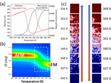
Status. There is increasing interest in understanding and exploiting materials that undergo first-order magnetic phase transitions and exhibit an interplay between the electronic, struc-tural and magnetic degrees of freedom [60–71]. Two important examples are colossal magnetoresistance [60] and giant mag-neto-caloric effect [61] materials, whose functional responses are associated with first-order magnetic phase transitions. A proto typical materials system is the equi-atomic ordered phase of FeRh that exhibits a first-order hysteretic metamagnetic phase transition from the low temperature antiferromagnetic (AFM) to the high-temperature ferromagnetic (FM) phase (see figure 8) [62–65]. In FeRh, there is no crystal symmetry change through the transition, but the unit cell volume expands by ~1%, demon-strating a significant coupling between the magnetism and struc-ture (figure 8(b)). Commensurate with this trans ition is a large change in electrical resistivity (figure 8(a)) and entropy. Because of its relatively simple structure and high trans ition temper-ature FeRh has become a test-bed for exploring the interplay of structural, magnetic and electronic phase transitions in metallic systems. In films, the phase transition is both hysteretic and rela-tively broad in temper ature, as seen in figure 8, where there is a co-existence of the AFM and FM phases in the transition region. This co-existence can be seen by x-ray nano-diffraction imaging (figure 8(c)) during the phase transition which shows a hetero-geneous transition in both warming and cooling. In FeRh, the phase inhomogeneity is at least partly associated with disorder where local regions undergo the transitions at different temper-atures and the domain sizes are typically sub-micron. This type of heterogeneous transition is a general response of this class of materials [60].
Another example of first-order magnetic transitions in metallic systems are alloys exhibiting martensitic phase trans-itions from a high-temperature cubic austenite phase to a low-temperature martensite phase with lower symmetry [66]. With appropriate doping there is an interplay between the structure, magnetism and electronic properties across the martensitic transformation. The complexity of these systems can be seen in off-stoichiometric alloys of full Heusler compounds, such as Ni2MnZ (Z = Sn, In, Ga, etc). When Co-doped and off-stoichiometric (e.g. Ni2−xCoxMn1+yZ1−y), these alloys can exhibit reversible martensitic phase transformations, mul-tiferroicity and phase competition that leads to spontaneous nanoscale magnetic inhomogeneity as seen in neutron small-angle scattering [66].
More generally, the interactions within strongly correlated electron systems and symmetry breaking often lead to ordered and/or coexisting states, such as charge ordering, supercon-ductivity, antiferro-, ferri- and ferro-magnetic order, ferroe-lectricity and magneto-electronic phase separation [60, 67]. A historically important example is magnetite, Fe3O4. At the
Verwey transition (TV = 123 K), Fe3O4 undergoes a metal-insulator transition with a lattice transformation from cubic to monoclinic structure with charge and orbital ordering. The phase transition proceeds by phase separation into coexisting and fluctuating metallic and insulating domains [66]. Such complex behaviour is ubiquitous in transition-metal oxides [60, 67–69], which often transition from an isotropic metallic FM state to an insulating AFM state upon charge and orbital ordering.
Beyond the fundamental interest in complex materials, there are opportunities in exploiting these highly active materials (as described for energy applications in section 13). The nature of the phase transition can be tuned by strain, pressure, chemical doping and temperature, as well as magnetic and electric fields. Because of the cross coupling of the order parameters, these materials are generally multiferroic. An understanding of new properties at the nanoscale in complex heterostructures [64], and their relationship to function, will lead to new applications in diverse areas, such as magnetic sensors and actuators, new classes of magnetic memory and recording (see section 11), magnetic refrigeration and energy storage (see section 13), as well as magnetic shape memory and barocaloric effects [61, 64, 67, 75]. A recent intriguing example is the demonstration of a large reversible caloric effect in FeRh thin films via a dual-stimulus multicaloric cycle in FeRh/BaTiO3 heterostructures [64]. By this approach, it is possible to overcome the irrevers-ibility in magnetocaloric cycles expected from the large hyster-esis of the FeRh phase transition (figure 8).
Current and future challenges. As highlighted above, the first-order phase transitions are generally characterized by hysteresis and it is common to see phase separation that can be both spontaneous and/or results from local disorder [60] lead-ing to a coexistence of various magnetic/structural/electronic phases on the micro- or nano-meter scale (figure 8). Progress in both the science and technological applications of materials requires a quantitative understanding of the phase coexistence in various classes of materials. Further, it is important to under-stand the nature of the boundary between the phases where competing orders may stabilize new phases or enable new properties, as seen in the paramagnetic metal to AFM insulator transition in V2O3. An intermediate electronic state is observed that is linked to the strain accommodation from coexistent structural phases [69]. Understanding such complex phase behaviour will require close coupling of synthesis, including studying mesoscale structures, theory and characterization of materials at the appropriate spatial and temporal scales. There are numerous examples where the phase separation is intrin-sic to the system [60, 66–69], spontaneously appearing as a result of competing interactions and can be a dynamic precur-sor of the phase transition. A current and future challenge is to understand the nature of the phase separation, both spatially and temporally, and the degree to which the phase separation is linked or possibly controlled by local structural variations (i.e. intrinsic versus extrinsic mechanisms).
Most studies of phase separation have been on bulk or extended film materials. A fascinating question is how these materials respond when the dimensionality of the material is
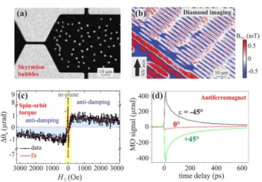
reduced, particularly to the scale of the phase heterogeneity [63, 70]. For FeRh films patterned into wires (figure 9(a)), whose widths are the same scale of the phase separation seen in figure 8, the measured first-order transition becomes strongly asymmetric [63] as seen in figure 9(b). For warming from the AFM to FM phase, the transition remains nearly continuous over a broad temperature range with small jumps in the resist-ance as local regions undergo the AFM-FM transition (similar to figure 8(a)). However, for cooling, there is a pronounced supercooling and an avalanche-like abrupt transition from the FM to the AFM phase. It is argued that this results from the robustness of the FM exchange to local strain and disorder in films when compared to the AFM exchange correlations and highlights additional complexity when the sample dimensions are reduced [63, 70]. The interplay of structural and magnetic correlations/disorder can dramatically alter their response for reduced dimensions and is not well understood or predictive at this time. This will be particularly important for many appli-cations where meso- or nano-scale devices are needed [64, 70] and as discussed in sections 11 and 12.
Advances in science and technology to meet challenges.
Progress both in the science and technological potential
resolved synchrotron-based scanning x-ray nano-diffraction (see figure 8(c)) and spectro-microscopy techniques, neutron scattering and transmission electron microscopy to name a few (see chapter 1 of [7] and section 6). These techniques are supplemented by recent developments of various nano-plas-monics approaches that allow enhancement and local control of optical fields down to the nanoscale (as highlighted in sec-tion 5) for optics-based spectroscopy and imaging techniques (e.g. see [64]). It will be of particular importance to develop techniques that can combine both high spatial and temporal resolution, such as x-ray photon correlation spectroscopy or various pump-probe techniques. Further information will be gained by moving into the ultra-fast regimes [65, 67], where phase transitions can be studied far from thermal equilibrium, and into investigating ultrafast dynamics, including different elementary interactions between spins, electrons and lattice (as highlighted in section 9). While ultrafast optical pump-probe techniques have been available for the last twenty years that can study the average temporal response of the magnetic/ electron order, there are increasing opportunities to explore the spatial distribution of magnetic/electron/structural order in the sub-ps time scales [65]. This will dramatically increase with the development of new femtosecond hard and soft x-ray scattering with x-ray free electron lasers and novel fs electron diffraction and imaging techniques [71].
Concluding remarks. The study of complex materials, such as FeRh, manganites and Heusler compounds [60–65] that undergo first-order phase transitions, provide exciting oppor-tunities for gaining an improved understanding of magne-tism and magnetic phase transitions. The interplay between multiple degrees of freedom and competing interactions can drive the system into complex mixed phases that further can be manipulated by confinement of the system. Understanding how the coupling of ferroic properties leads to highly non-linear responses to external perturbation should make a broad
Figure 9. Image of a patterned FeRh stripe (scale bar is 5 µm).
The inset shows discrete steps in the order parameter upon heating corresponding to the transition in uncorrelated regions of the sample. Upon cooling, the transition proceeds primarily through a single event. Reproduced from [63]. CC BY 4.0.
Figure 8. Magnetic, transport and structural properties of FeRh
thin films. (a) Net magnetic moment versus temperature of a film and resistance versus temperature of a 1.1 µm wide stripe patterned
from the same film. (b) X-ray diffraction results for the FeRh (002) diffraction peak on warming showing the transition from the AFM to FM phase as highlighted by the dashed box. (c) X-ray nano-diffraction warming and cooling cycles. The image area is 4 × 4 µm2 and blue corresponds to the AFM phase and red the FM
phase. (a) Reproduced from [63]. CC BY 4.0. (b), (c) are courtesy of Martin Holt, Yong Choi, Jong-Woo Kim, Philip Ryan and David Keavney at the Advanced Photon Source (APS), Argonne National Laboratory. The data in (c) was acquired at beamline 26-ID at the APS.
6. Advances in magnetic characterization Peter Fischer1
1 Lawrence Berkeley National Laboratory and University of California, Santa Cruz
Status. The primary goal of magnetism research and technol-ogy is to understand, discover and tailor the static properties and the dynamic behavior of spin textures that can find appli-cations with advanced magnetic materials in devices showing novel functionalities [72]. To achieve those goals, the scien-tific topics that need to be addressed are intimately related to spin textures (section 4) spanning multiple length and time scales, and the excitations of spins and their interactions across various energy scales. The phenomena to be studied result from the competition of various magnetic interactions; the most prominent being the symmetric and antisymmetric exchange, anisotropy and dipolar interactions. Novel and unexpected magnetic properties, behaviors and functionalities can arise specifically at interfaces between various phases and components, as a result of confinement down to the nanoscale where quantum behavior dominates, and in the dynamics of spin textures [2]. Broken symmetries at magnetic interfaces (section 1), quantum matter features and spin dynamics are therefore primary targets for guiding future directions in advanced magn etic characterization. The open questions and the associated experimental and theoretical challenges are manifold. For example, how can we understand, manipu-late and design the complexity that comes with interfaces or an increased dimensionality, i.e. with spin textures in three dimensions? How can we combine experimentally and theor-etically the ultrafast and ultrasmall magnetism world, e.g. the flow of spin currents through interfaces?
A vast amount of numerous and powerful methodologies to characterize magnetic materials is available nowadays [73], enabling us to increase our fundamental understanding of magnetic phenomena and their utilization in novel tech-nologies. Some examples that testify to the achievements are: the spin of a single electron can be detected in a single Si transistor with single electron spin resonance [74]; Spin-polarized scanning tunneling microscopies allow us to image and manipulate individual spins with atomic spatial resolution [75]; the unexpected discovery of demagnetization in ferro-magnetic nickel on a fs time scale (section 9) has progressed towards the feasibility of all-optical spin manipulation in THz spintronic devices [76]; and x-ray dichroism effects in magn-etic systems allow us to measure quantitatively ground state spin and orbital magnetic moments with elemental specificity and high sensitivity [77].
Current and future challenge. Manipulating the spin, and its associated spin currents, can be achieved in many ways, which can impact the requirements for advanced characterization techniques. Applying external magnetic fields so as to force the magnetic moment to align with the field direction is still the primary concept used e.g. in magnetic information storage
technologies (section 11). However, the limitations with scal-ing and the energetic inefficiencies, due to runnscal-ing electri-cal currents for generating magnetic fields, are fueling active research in finding different ways of controlling magnetism. Using electric fields to switch magnetization in multiferroic materials, utilizing pure spin currents or at least spin polarized currents in spin-orbitronics, and ultimately all-optical control of magnetism are the most prominent research directions today (section 9). The challenges for characterization are the ability to study with high spatial and temporal resolution, ultimately down to the nm and fs regimes, respectively, and in–operando as a function of applied external parameters, including elec-tric and heat currents, elecelec-tric and magnetic fields, ultrashort optical pulses, the statics and dynamics of the underlying microscopic spin textures. A detailed, i.e. highly spatial, and temporal resolution characterization of spin textures at buried interfaces and specifically the spin dynamics at such interfaces, or more generally, the behavior of spins in 3D nanoscale sys-tems, is still elusive. Whereas, independently, fundamental time and spatial scales for magnetic systems can be studied, a combined spatio-temporal characterization at atomic length and ultrafast (fs) time scale or ultimately a full multimodal/ multidimensional (space, time, polarization, external param-eters) methodology remains a future challenge. Although not generically a characterization tool (see figure 10, for instance), advanced computational approaches to investigate spin tex-tures across multiple length and time scales can provide guid-ance towards reaching those ultimate experimental limits.
Advances in science and technology to meet challenges.
In the following, we will present some selected examples of current research showing both the current state-of-the-art and the ongoing developments in magnetic metrologies. Imaging magnetic microstructures provides an insight into fundamental processes in magnetic materials. Albeit magneto-optical effects, such as the Kerr or Faraday effects, provide magnetic contrast and laser pulses are in the fs regime (section 7), the wavelengths of visible light pose severe limitations to address the nanoscale. X-rays, specifically polarized soft x-rays using x-ray dichro-ism effects as magnetic contrast (see above), can overcome this limitation. Whereas, x-ray optics have demonstrated the abil-ity to push magnetic x-ray microscopy into the ten nm regime, recent developments with x-ray imaging in reciprocal space, specifically harnessing the increased transversal (and longitu-dinal) coherence at next generation x-ray light sources, such as x-ray free electron lasers or diffraction limited storage rings, have the potential to not only push the spatial resolution into the single digit nm regime, but to provide, at the same time, snap-shot images of fs spin dynamics, and with inherent elemental sensitivity and quantitative information.
A recent study with soft x-ray ptychography [78] has dem-onstrated a spatial resolution around 10 nm for imaging the domain pattern in a SmCo5 thin film. In addition, the analysis of the heavily oversampled data allows us to retrieve informa-tion of both the magnetic x-ray amplitude and the magnetic x-ray phase (figure 11).
Detecting the magnetic x-ray phase could open significant advantages in the future. A large magnetic phase contrast appears below the x-ray absorption edge that significantly reduces radiation damage at x-ray free electron laser (XFEL) experiments. Further, the magnetic sensitivity could be sub-stantially increased if combined with x-ray interferometric measurement setups, which will become feasible again at the next generation x-ray sources with full coherence.
Those sources will also enable the study of collec-tive dynamics, e.g. by x-ray photocorrelation spectroscopy (XPCS) and the observation of fluctuating speckle patterns, which are directly correlated to fluctuations of relevant order parameters in real space [79]. Correlating the charge, spin and orbital orders, across a wide range of length and time scales that XPCS can address, will provide insight into the energy landscape and the interactions in magnetic materials.
Magnetic Fourier transform x-ray holography is another promising tool that has the potential to combine the ultrasmall and the ultrafast regime of nanomagnetism investigations. Recently, a first experiment has demonstrated a so-called two-color setup, where the magnetic response of two different components in a complex heterostructure was recorded simul-taneously at an XFEL source [80].
One of the frontiers in magnetic characterization is the fundamental understanding of spin currents, and specifically their fast dynamics. The ultimate goal is to study spin current as they locally transverse an interface. However, this requires high spatial resolution and a high sensitivity to detect small signals and at buried interfaces. A significant increase in sen-sitivity was recently accomplished through the implementa-tion of a long term synchronizaimplementa-tion of a pump-probe setup between the clock frequency of the x-ray pulses from a syn-chrotron and the detection of the local XMCD response with a scanning transmission x-ray microscope [81].
Access to buried interfaces is related to the ability to char-acterize spin textures in three dimensions with nanoscale spa-tial resolution (sections 1 and 3). Interface sensitivity can also be achieved in certain reflection geometries or via the use of moving x-ray standing waves through the interface of interest
This can be achieved with electrons, e.g. in a TEM [82] but also with x-ray vortex beams [83]. Novel magnetic spectro-microscopies reaching directly into highly excited states, or novel ways to manipulate spins on the atomic scale (magnetic nanotweezers), can be envisioned.
A very promising characterization tool with high potential are nitrogen vacancy (NV) center scanning probe microsco-pies, which provide quantitative and highly sensitive measure-ments of the stray magnetic field emanating from a nanoscale spin texture. Ultimately, the spatial resolution with NV center microscopies is only limited by the atomic size of the probe [84].
Concluding remarks. Advances in magnetic metrology are key to gain insight into magnetism down to the fundamental length and time scales, but also to enable applications towards novel technological applications. New opportunities will arise, taking into account non-uniform, aperiodic spatial and tempo-ral spin structures across multiple scales, broken symmetries at interfaces and the complementarity of spins and magnons (section 10) resembling fermionic versus bosonic behavior.
Acknowledgments
PF is supported by the US Department of Energy, Office of Science, Office of Basic Energy Sciences, Materials Sciences and Engineering Division, under Contract No.
DE-AC02-Figure 11. Reconstructed soft x-ray ptychography magnetic
amplitude (top row) and phase (bottom row) images of the domain pattern in a SmCo5 thin film recorded with left circularly polarized
x-rays at various photon energies around the Co L3 absorption edge.
Reprinted from [78], with the permission of AIP Publishing.
Figure 10. Characterization is at the nexus between discovery and
understanding, and application of magnetic materials and their underlying spin textures.