HAL Id: hal-02448489
https://hal.archives-ouvertes.fr/hal-02448489
Submitted on 5 Jan 2021HAL is a multi-disciplinary open access archive for the deposit and dissemination of sci-entific research documents, whether they are pub-lished or not. The documents may come from teaching and research institutions in France or abroad, or from public or private research centers.
L’archive ouverte pluridisciplinaire HAL, est destinée au dépôt et à la diffusion de documents scientifiques de niveau recherche, publiés ou non, émanant des établissements d’enseignement et de recherche français ou étrangers, des laboratoires publics ou privés.
Silver nanoparticles as a key feature of a plasma
polymer composite layer in mitigation of charge
injection into polyethylene under dc stress
Laurent Millière, K Makasheva, Christian Laurent, Bernard Despax, Laurent
Boudou, G. Teyssedre
To cite this version:
Laurent Millière, K Makasheva, Christian Laurent, Bernard Despax, Laurent Boudou, et al.. Silver nanoparticles as a key feature of a plasma polymer composite layer in mitigation of charge injection into polyethylene under dc stress. Journal of Physics D: Applied Physics, IOP Publishing, 2016, 49 (1), pp.015304. �10.1088/0022-3727/49/1/015304�. �hal-02448489�
1
Silver nanoparticles as a key feature of a plasma polymer composite layer
in mitigation of charge injection into polyethylene under DC stress
L. Milliere, K. Makasheva, C. Laurent, B. Despax, L. Boudouand G. Teyssedre*
LAPLACE (Laboratoire Plasma et Conversion d’Energie), Université de Toulouse; CNRS, UPS, INPT; 118 route de Narbonne, F-31062 Toulouse, France
*Corresponding author: gilbert.teyssedre@laplace.univ-tlse.fr
Keywords—polyethylene, nanocomposites, silver nanoparticles, plasma processes, HVDC, charge injection, space charge mitigation
ABSTRACT
The aim of this work is to limit charge injection from a semi-conducting electrode into low density polyethylene (LDPE) under DC field by tailoring the polymer surface using a silver nanoparticles-containing layer. The layer is composed of a plane of silver nanoparticles embedded in a semi-insulating organosilicon matrix deposited on the polyethylene surface by a plasma process. Size, density and surface coverage of the nanoparticles are controlled through the plasma process. Space charge distribution in 300 m-thick LDPE samples is measured by the pulsed-electroacoustic technique following a short term (step-wise voltage increase up to 50 kV/mm, 20 min in duration each, followed by a polarity inversion) and a longer term (up to 12 hours under 40 kV/mm) protocols for voltage application. A comparative study of space charge distribution between a reference polyethylene sample and the tailored samples is presented. It is shown that the barrier effect depends on the size distribution and the surface area covered by the nanoparticles: 15 nm (average size) silver nanoparticles with a high surface density but still not percolating form an efficient barrier layer that suppress charge injection. It is worthy to note that charge injection is detected for samples tailored with (i) percolating nanoparticles embedded in organosilicon layer; (ii) with organosilicon layer only, without nanoparticles and (iii) with smaller size silver particles (<10 nm) embedded in organosilicon layer. The amount of injected charges in the tailored samples increases gradually in the samples ranking given above. The mechanism of charge injection mitigation is discussed on the basis of complementary experiments carried out on the nanocomposite layer such as surface potential measurements. The ability of silver clusters to stabilize electrical charges close to the electrode thereby counterbalancing the applied field appears to be a key factor in explaining the charge injection mitigation effect.
2 1. INTRODUCTION
Optimization and valorization of green electrical energy production is one of the most important economic development concerns in the world. However, as energy production sites are often far from consumption sites, there is a need to transport energy over long distances, including sometimes undersea connections. In this context High Voltage Direct Current (HVDC) links represent several advantages over HVAC lines like the reduction in energy losses along with the absence of reactive power compensation stations [1]. Polyethylene-based materials are used for long in the insulation of HVAC extruded cables and accessories where they gradually replaced oil-paper insulations. In spite of this experience in the field, HVDC extruded cables still suffer from reliability problems due to the accumulation of electric charges forming internal space charge in the polymer bulk [2, 3]. This phenomenon creates an internal electric field distribution different from the design field that can trigger local damages to the structure which leads ultimately to breakdown [4, 5]. In theory, polyethylene with its wide band gap of 8.8 eV[6] should prevent charge injection from any conducting or semi-conducting electrodes. In reality, electronic carriers of positive and negative polarities are injected from the contact electrode/polymer and are detected as space charge using space charge measurement techniques [7]. Charge injection has been reported both in laboratory experiments carried out on flat samples with semi-conducting (SC) contacts to mimic the situation in cables and in real cables where a semi-conducting screen (carbon black doped thermoplastic) is in contact with the polymer [8]. This charge injection process is presumably due to energy states enabling carriers to by-pass the potential barrier at the SC/dielectric interface[9]. Moreover, extruded cables production is mainly based on cross-linked polyethylene (XLPE) owing to its outstanding thermo-mechanical stability. The crosslinking process generally uses peroxides as initiator, leading to the formation of by-products which substantially contribute to space charge features of the material when compared to low density polyethylene (LDPE) [10]. Many papers have been published over the last two decades on the impact of additives and residues on space charge in polyethylene materials, especially in XLPE. In going from LDPE to XLPE a switch from homocharge-dominated to heterocharge-dominated space charge profiles occurs, which can be roughly understood as a switch from injection-dominated charge build-up to ionic charge build-up originating from crosslinking residues.
Several methods for improving the performances of polyethylene-based insulation of HVDC cables by reducing space charge build-up have been investigated. Strategies are envisaged either at the source of the charges or at the level of their dispersion in the material. Expelling cross-linking by-products, which are volatile molecules, by heating the system is in principle one of the solutions to reduce the amount of ionic carriers in XLPE. However it may become very demanding energetically for thick insulations as in high voltage cables. So, ongoing researches address the development of processes limiting the amount of by-products. Most of the attempts for reducing the amount of space charge concern the modification/improvement of the bulk material. Dispersion of nano-fillers into the polymer bulk is being deeply investigated nowadays [11], for example in LDPE with dispersion of
3
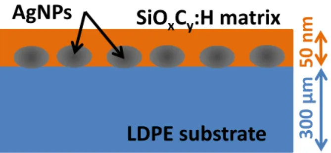
nano TiO2 [12], Al2O3 [13], montmorillonite [14] and MgO [15] particles. The general trend is a mitigation effect of the amount of space charge without clear evidence on the mechanism due to the complexity of the nanocomposite materials and the variability of results [16].To our knowledge, few studies focus on the polymer/electrodes interface properties to tune charge injection effect. Tailoring the interfacial properties of the insulation could be a way to control the generation of electronic carriers. The most common studies consist in a modification of the polymer sample interface by fluorination with a F2/N2 mixture [17]. Charge injection mitigation was reported to be due to the presence of deep traps into the fluorinated layer that can block or shield further charge injection. Following a different strategy, we recently reported [18] on charge injection mitigation when a thin composite layer containing silver nanoparticles (AgNPs) was deposited on the surface of polyethylene as shown in Figure 1. A drastic effect was observed and attributed to the presence of AgNPs acting as deep traps. In this paper, we extend the analysis in order to find out which features of the nanocomposite layer are playing key role in charge injection mitigation. The paper is organized along the following lines. We first give the experimental details describing the substrate preparation, plasma deposition process and methods for physico-chemical and electrical characterization. We discuss in a second part the impact of the process parameters on the distribution of the size and density of the AgNPs contained in the composite layer. Space charge patterns under different protocols for DC voltage application are discussed in a third part by changing the characteristics of the composite layers. Results are discussed in a fourth part of the paper.
Figure 1. Schema of polymer surface tailored by a AgNPs/SiOxCy:H nanocomposite layer.
2. EXPERIMENTAL DETAILS
2.1. Substrate preparation
Polymer substrates of LDPE were produced from antioxidant-free pellets, as specified by BOREALIS, molded at 155°C under 3 bars for 20 minutes. The final samples were disks of 7 cm in diameter and 300 ± 10 µm in thickness. The LDPE substrates were subsequently outgassed for 12 h under vacuum (0.06 Pa) at 23°C for removing volatiles molecules and water. Indeed it has been shown that even using antioxidant-free polyethylene films, space charge can be detected originating from the material bulk and giving rise to spurious effect when investigating charge injection from the electrodes. When conditioning the samples under vacuum for a given time, injection phenomena can be revealed
LDPE substrate
3
0
0
µm
5
0
n
m
4
through the detection of homocharge (charge of the same sign as the nearby electrode) above a field level of the order of 10 to 15 kV/mm using conventional space charge detection techniques [19]. The vacuum pretreatment conditions also conform to the low pressure plasma deposition process described below.
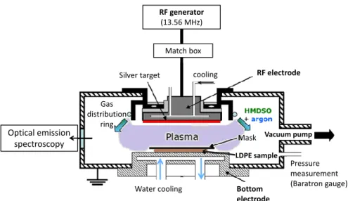
2.2. RF plasma process
The nanocomposite layer is synthetized in a low pressure plasma reactor enabling sputtering from a silver target and plasma polymerization of hexamethyldisiloxane (
HMDSO - [CH
3]
6Si
2O
) as twoindependent steps in the same chamber. Details of the process can be found elsewhere [20, 21]. The plasma reactor is schematized in Figure 2. The asymmetrical electrodes configuration of this capacitively coupled radio-frequency (RF, f = 13.56 MHz) driven discharge leads to a self-bias of the smaller electrode. The LDPE substrate is clamped on a temperature-controlled substrate holder (bottom electrode) connected to the ground. The RF power is transmitted to a silver target (smaller electrode) located 4 cm above the sample. The plasma is initiated in pure argon at pressure of 5.33 Pa after pumping the chamber for 12 hours at very low pressure of 0.06 Pa. Owing to the asymmetrical design of the electrodes, argon ions of the discharge are accelerated by the self-bias voltage towards the silver electrode where they sputter silver atoms forming nanoclusters on the LDPE sample surface. The size distribution and surface density of the AgNPs can be controlled by changing the experimental parameters: power of the discharge (i.e. self-bias voltage), discharge pressure and sputtering time. A range of parameters were chosen for our study as being 40, 60 and 80 W for the discharge power (corresponding to self-bias voltages -725, -850 and -970 V, at 8.00 Pa), 5.33 and 8.00 Pa for the gas pressure, the deposition time being constant (5 s). In a second step, HMDSO is introduced into the chamber with the plasma powered on. This implies that the silver electrode is quickly totally covered by a thin polymer layer therefore preventing from silver sputtering. HMDSO partial pressure is controlled through a pulsed flow, argon partial pressure is maintained at 5.33 Pa and the RF power is maintained at 80 W. The thickness of the SiOxCy:H layer deposited on top of the AgNPs previously formed at the LDPE surface is controlled by the deposition time fixed at 60 s in our study. The LDPE samples are hidden behind a mask for the time of plasma process stabilization and then exposed to the plasma during the deposition time by removing the mask. It allows controlling the short deposition times used in this experiment. The processes of silver sputtering and SiOxCy:H deposition are monitored by optical emission spectroscopy through the intensity ratio of the emission lines of silver and argon excited atoms (λAg = 546.6 nm and λAr = 549.6 nm, respectively) [21].
5
Figure 2. Schema of plasma reactor.
2.3. Physico-chemical characterization methods
The chemical structure of the layers was analyzed through Fourier Transform Infra-Red spectroscopy in Attenuated Total Reflectance mode (ATR-FTIR) in the range 400-4000 cm-1 using a Brucker Vertex 70 spectrometer. Images of the nanocomposite layers were obtained by Scanning Electron Microscopy (SEM). The thicknesses of the nanocomposite layers were inferred from SEM observations of the samples in Energy Dispersive X-ray spectrometry mode (EDX) in a cross-section view. Some of samples were produced with the AgNPs layer only, without SiOxCy:H coating in order to observe the silver clusters and determine their parameters. The surface density, covered area (fraction of LDPE sample area covered by AgNPs) and size distribution were deduced after image processing. The latter was performed with Gatan DigitalMicrograph® software by application of filters associated with a selective numeral analysis.
2.4. Space Charge Measurements Method and Protocol
The Pulsed Electro Acoustic (PEA) technique was used for space charge measurements. The principle of the PEA technique consists in detecting acoustic waves generated by internal charges under the Coulombic influence of a pulsed electric field [22]. The equipment is composed of a high voltage direct current supply connected to a semi-conducting (SC) electrode made of carbon black-doped polymer. The pulse generator is also connected to the high voltage through a decoupling capacitance. An aluminum electrode is used as the ground electrode where the acoustic waves are detected. Samples are sandwiched between the two electrodes of the PEA system without further metallization. The PEA cell is installed in a thermo-stated oven and all measurements were realized at 25°C. To obtain an exploitable signal, the acoustic response to excitation by 600 V amplitude pulses at 1 kHz frequency is averaged for 60 s. The spatial resolution of the set-up is 25 µm. Deconvolution of the signal was done by using software developed in our laboratory. The samples were tested following a
Silver target Gas distribution ring Optical emission spectroscopy Match box RF generator (13.56 MHz) RF electrode cooling Mask LDPE sample
Water cooling Bottom
electrode
Pressure measurement (Baratron gauge) Vacuum pump
6
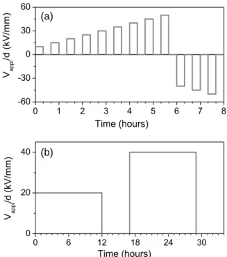
protocol depicted in Figure 3. It consists of different steps of polarization, each followed by a depolarization period. In a short term protocol (Figure 3(a)) the DC field is increased from 10 kV/mm to 50 kV/mm by steps of 5 kV/mm (corresponding to a positive voltage applied to the HV electrode). The voltage is maintained at each step for 20 min, followed by a depolarization step for 20 min. After the last positive step at 50 kV/mm (positive voltage applied to the SC electrode), the applied stress was reversed to -40 kV/mm with a subsequent increase to -50 kV/mm. PEA profiles were recorded every 60 s in the polarization and depolarization steps at each voltage level. In a longer term protocol (Figure 3(b)) we used two steps of 20 kV/mm and 40 kV/mm applied for 12 hours each (positive voltage applied to the SC electrode). Each step is followed by a depolarization period lasting for 5 hours. PEA profiles were recorded every 150 s. The dynamics of the space charge is revealed through color maps showing the measured charge density (color scale) in a 2D-representation where the x-axis is the time (associated with the applied voltage through the experimental protocol) and the y-axis the position between anode and cathode.
Figure 3. Short (a) and longer (b) term protocols for space charge measurements.
2.5. Surface potential measurements
Electrical properties of the samples were investigated by surface potential measurements following charging of the material by corona discharge. Charging was achieved applying a DC voltage of 3500 V during 10 s on a needle electrode installed at 5 mm from the sample surface. Potential profiles were measured using a Kelvin probe by scanning the surface along different axes in steps of 5 mm at different times after charging: 0, 3, 15 and 60 minutes. All measurements were carried out in air at room temperature. 0 1 2 3 4 5 6 7 8 -60 -30 0 30 60 V appl /d ( kV /m m ) Time (hours) (a) 0 6 12 18 24 30 0 20 40 V appl /d ( kV /m m ) Time (hours) (b)
7
3. PHYSICO-CHEMICAL CHARACTERIZATION
3.1. Nanoparticles size and surface density as a function of experimental parameters
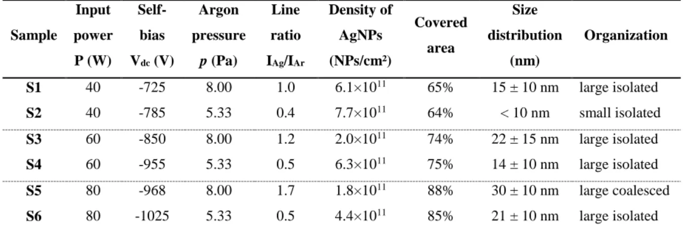
The plasma operation conditions along with the results from the analysis of size, surface density and organization of sputtered AgNPs on the LDPE samples are summarized in Table I. Three values of the input power (40, 60 and 80 W) and two values of the argon pressure (8.00 and 5.33 Pa) were used in this experiment. The corresponding self-bias voltages are also given. The self-bias voltage is related to the asymmetric nature of capacitively-coupled discharges [23]. It is set up at the driven electrode and results from the DC voltage drop between the bulk plasma and the electrodes across the plasma sheaths connecting the driven electrode to the ground. It is negative in the usual case and since the voltage drop across the sheaths is inversely proportional to the sheath capacitances, the sheath with smaller area (smaller electrode) has smaller capacitance and therefore a larger voltage drop. It scales up with the injected power, at a constant pressure, as confirmed in this experiment (Table I), and is at the origin of the acceleration of argon ions towards the silver target, finally bombarding it. As the ion dynamic is strongly involved in the sputtering process, the gas pressure is the second important parameter after the injected power in this process. A gas pressure increase might influence the silver sputtering in the following ways: (i) through an increase of the plasma density, thus the ion density, if quasi-neutrality of the plasma is considered; (ii) through the plasma sheath close to the smaller electrode, mainly through its width and its nature (collisional or collisionless) and (iii) through the effect of scattering of sputtered atoms. Our results show that for a fixed injected power the self-bias voltage decreases when increasing the gas pressure. It is due to the thinner plasma sheath close to the powered electrode, when the gas pressure is increased, that will have a larger capacitance per unit area, thus setting up a smaller self-bias voltage. The most appropriate way to follow the plasma behavior in order to relate it to the plasma deposition process is through optical emission spectroscopy of the plasma glow emission, as performed in this work. The evolution of line intensity ratio of IAg(546.6nm) to IAr(549.6nm) gives an image of the Ag-amount in the plasma which can be related to the Ag-volume fraction deposited on the substrate. The higher the line intensity ratio, the higher the Ag-volume fraction is. The variation of the line intensity ratio (IAg(546.6nm)/IAr(549.6nm)) as a function of the injected power or the gas pressure is recorded for each deposition, since this kind of charts constitutes useful data to obtain reproducible results. According to the performed analysis three main categories of AgNPs can be identified (Table I): (i) small isolated AgNPs; (ii) large isolated AgNPs; and (iii) large coalesced AgNPs. This classification will be used hereafter. All the samples used for space charge measurements were covered by an organosilicon SiOxCy:H thin layer after the deposition of the layer of AgNPs.
8
Table I. Experimental parameters for silver sputtering and characteristics of deposited AgNPs.
Sample Input power P (W) Self-bias Vdc (V) Argon pressure p (Pa) Line ratio IAg/IAr Density of AgNPs (NPs/cm²) Covered area Size distribution (nm) Organization S1 40 -725 8.00 1.0 6.1×10¹¹ 65% 15 ± 10 nm large isolated S2 40 -785 5.33 0.4 7.7×10¹¹ 64% < 10 nm small isolated S3 60 -850 8.00 1.2 2.0×10¹¹ 74% 22 ± 15 nm large isolated S4 60 -955 5.33 0.5 6.3×10¹¹ 75% 14 ± 10 nm large isolated S5 80 -968 8.00 1.7 1.8×10¹¹ 88% 30 ± 10 nm large coalesced S6 80 -1025 5.33 0.5 4.4×10¹¹ 85% 21 ± 10 nm large isolated
Figure 4. SEM images in plan-view of the AgNPs layers deposited on LDPE substrate S1 (large isolated), S2 (small isolated) and S5 (large coalesced). SEM cross-section image in EDX mode of the AgNPs/SiOxCy:H
composite layer on the LDPE substrate S1t, containing the large isolated AgNPs presented on S1 image.
Figure 4 shows examples of each of the above identified categories of as-deposited AgNPs on the LDPE surface without SiOxCy:H cover layer
,
referred as to S1 (large isolated AgNPs), S2 (small isolated AgNPs) and S5 (large coalesced AgNPs). A cross-section view image of the AgNPs/SiOxCy:H nanocomposite stack on the LDPE surface, containing the large isolated AgNPs presented on S1 image, is also shown in EDX mode (bottom right panel, referred as to S1t in Figure 4). For sample S1, the AgNPs size span from 5 to 25 nm with an average size of 15 nm, the particles surface density being 6.4 × 10¹¹ NP/cm2 giving a surface covered area of 65%. Particles appear with irregular shape however, well isolated from each other. Sample S2, which has been prepared under a lower pressure (p = 5.33 Pa) for the same discharge power (P = 40 W), exhibits AgNPs of much smaller diameters (<10 nm) with larger surface density of 7.1 × 10¹¹ NP/cm2 and covered surface area of the same order as in sample S1. Sample S5 which has been prepared under the same pressure (p = 8.0 Pa) as sample S1 but for a higher discharge power (P = 80 W) exhibits much larger particles size spanning from 20 to 40 nm, with a density of 1.8 × 10¹¹ NP/cm2 and a covered surface area of 88%. The clusters appear coalesced with wormlike shape. The later feature has already been reported for other type of metal9
clusters (gold and/or cobalt clusters) embedded in fluorocarbon [24] or hydrocarbon matrices [25]. These features of the AgNPs are in agreement with the fact that, for a given deposition time, the amount of deposited silver increases with the discharge power or the gas pressure. The cross-section view shown in S1t allows a precise measure of the thickness of the nanocomposite layer (54 nm in the present example) which has been confirmed by profilometer measurements. Considering a size of 15 nm for the AgNPs, as deduced from the SEM image (upper left panel – S1), the nanocomposite layer can be represented by two regions with the first one consisting of AgNPs embedded in organosilicon matrix of thickness of 15 nm, and the second region of only organosilicon layer with thickness estimated to 35 nm.
3.2. Physico-chemical characterization of the composite layer
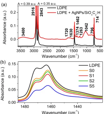
Figure 5(a) represents FTIR spectra of LDPE sample with and without any coating. Typical for LDPE surface chemical bonds [26], the four main peaks (see Table II): rocking r(CH2) at 714cm-1, bending
(CH3) at 1374cm-1 and (CH3) 1462cm-1, and the two stretching g(CH2) at 2843cm-1 and a(CH2) at 2916cm-1 are identified on the LDPE reference spectrum. No oxidized groups have been recorded after the vacuum preconditioning. The samples tailored with AgNPs/SiOxCy:H plasma polymer stack have many broad bands attributed to various chemical bonds in the range 800 cm-1 to 1263 cm-1 such as Si-O, Si-C, O-C and O-H. The band at 1042 cm-1 is associated with Si-O-Si asymmetric stretching mode in a silicon suboxide environment. The contribution at 1020 cm-1 is more probably ascribed to CHx(x<2)-Si wagging mode [20, 21].
Figure 5. ATR-FTIR spectra of samples: (a) reference LDPE and sample S1 (plane of AgNPs covered by an organosilicon layer); (b) focus on δ(CH2) bond at 1462 cm-1 for LDPE reference sample, samples S0 (LDPE
covered with only organosilicon layer), S1 (large isolated AgNPs covered by SiOxCy:H), S2 (small isolated
AgNPs covered by SiOxCy:H) and S5 (large coalesced AgNPs covered by SiOxCy:H).
3500 3000 2500 2000 1500 1000 500 0.0 0.1 0.2 A = 0.35 a.u. 1630 1720 3400 796 1042 1263 2916 714 1462 1374 A b so rb a n ce ( a .u .) Wavenumber (cm-1) LDPE LDPE + AgNPs/SiOxCy:H 2843 A = 0.39 a.u. (a) 1480 1460 1440 0.00 0.05 0.10 0.15 A b so rb a n ce ( a .u .) Wavenumber (cm-1) LDPE S0 S1 S2 S5 (b)
10
Table II. Band assignment of the FTIR spectra of LDPE and LDPE-AgNPs/SiOxCy:H samples.
Bond Wavenumber (cm-1) Vibrational assignment
γr(CH2) 714 rocking
CH3 in SiCH3 796 symmetrical stretching
SiOC in SiOCH3 800-850 rocking
Si-H 800-950 stretching
Si-O-Si 1042 asymmetrical stretching
Si-CHx(x<2)-Si 1020 wagging
C-H in SiCH3 1263 symmetrical deformation
δ(CH3) 1374 bending
C-H in SiCH3 1410 rocking
δ(CH2) 1462 bending
C-C=O and C=O 1630-1720 stretching
νg(CH2) 2843 stretching
C-H in CH3 2904 asymmetrical stretching
νa(CH2) 2916 stretching
O-H (free and
associated) 3200-3600 stretching
Silver nanoparticles were not directly detected by ATR-FTIR analysis but their presence on LDPE surface contributes to the intensity decrease of CH2 and CH3 peaks (Figure 5(b)) by the exerted light filtering effect. The intensity of LDPE vibrational peaks is inversely proportional to the size and the surface covered by AgNPs (Table I). The highest intensity is recorded for the LDPE sample alone, than for the LDPE sample covered with only organosilicon layer. The peak intensity decreases with increasing the AgNPs mean size. In presence of AgNPs, when they are coalesced as for sample S5, the intensity ICH2(LDPE) at 1462 cm-1 is twice smaller as compared to the intensity of the same band for the S2 sample (small isolated AgNPs). For the same surface covered area, the CH2 peak intensity increases when the particle size is smaller.
4. SPACE CHARGE MEASUREMENTS
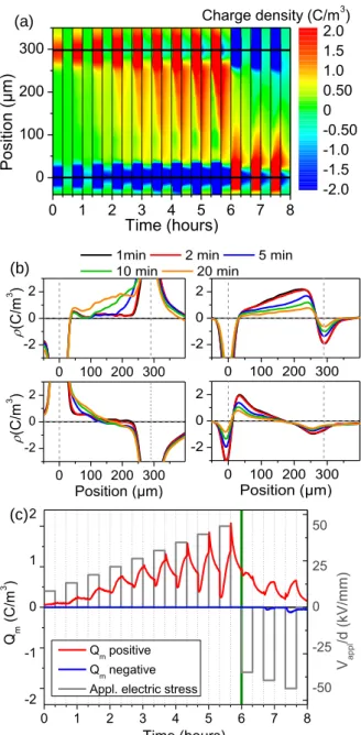
4.1. Space charge in reference LDPE sample
Figure 6(a) shows the space charge density along the protocol defined in Figure 3(a) for a 300 m-thick degassed bare LDPE sample. It is typical of the behavior of treated-LDPE sample with a distribution dominated by charge injection and a space charge density below 10 C/m3 [19]. For a positive voltage polarity, the distribution is dominated by charge injection from the SC electrode (position 300 µm in Figure 6(a)) and a bulk space charge density below 2 C/m3. The positive charges begin to be injected at 20 kV/mm with an increasing density up to the maximum applied field (50 kV/mm). Negative charge injection from the aluminum electrode is not detected (position at 0 µm on Figure 6(a)). This is in accordance with the results reported in the literature [27] as regards the efficiency for charge injection of various contacts. The Al/polyethylene contact is weekly injecting for negative charges when compared to the SC/polyethylene contact for positive charges. Also, it was shown experimentally that the mobility of negative charge is much lower than that of positive carriers
11
in LDPE [7]. For these reasons the space charge patterns are dominated by positive carriers. Models describing bipolar charge transport account for this behavior [27].
Figure 6. Space charge dynamics in reference LDPE sample along the short term protocol: (a) 3D plot of space charge dynamics, (b) charge density profiles during polarization (left) and depolarization (right) for the steps at 50 kV/mm under positive (top) and negative (bottom) applied voltages, and (c) averaged positive and negative charge densities along the protocol.
When a negative voltage polarity is applied (polarity reversal), both positive and negative charge distributions are observed. It must be noted that in this case, the first negative voltage step is applied with a preexisting positive charge adjacent to the top electrode (cathode). This positive charge magnifies the cathode field by about 5 kV/mm therefore favoring negative charge injection at SC/LDPE contact. Increasing the negative voltage leads to a bi-polar space charge distribution clearly visible in the distributions recorded at 45 kV/mm and 50 kV/mm, where a net-zero charge density-domain is revealed in the middle of the sample. A dynamic front of positive charge injected from the
0 1 2 3 4 5 6 7 8 0 100 200 300 Time (hours) P o sit io n ( µ m ) -2.0 -1.5 -1.0 -0.50 0 0.50 1.0 1.5 2.0 Charge density (C/m3) (a) (c) 0 1 2 3 4 5 6 7 8 -50 -25 0 25 50 Qm ( C /m 3 ) Time (hours) Qm positive Qm negative Appl. electric stress -2 -1 0 1 2 V appl /d ( kV /m m ) 0 100 200 300 -2 0 2 0 100 200 300 -2 0 2 Position (µm) -2 0 2 0100 200 300 -2 0 2
1min 2 min 5 min
10 min 20 min (b) 0 100 200 300 -2 0 2 0 100 200 300 -2 0 2 (C /m 3 ) Position (µm) (C /m 3 )
12
Al electrode is visible. One should keep in mind that in any space charge measurement, the apparent charge density, would it be zero charge density, can be the result of a net value of overlapping positive and negative charge distributions. The origin of negative charges seen after polarity reversal near the SC electrode is not straightforward. It seems to be due to a negative charge injection from the SC cathode all the more that the cathode field is intensified as mentioned above.
Figure 6(b) shows the example of the charge dynamics at 50 kV/mm before and after the polarity inversion, in polarization and depolarization. The build-up of the positive charge during polarization at 50 kV/mm is clearly revealed as well as the positive charge decay during depolarization. Upon polarity reversal, the build-up of the bipolar space charge is evidenced under polarization as well as its decay in depolarization. In order to be more quantitative and for comparison purpose, we have represented in Figure 6(c) the evolution of the absolute value of the internal charge along the voltage protocol. To this aim, we have integrated the charge over the insulation thickness, differentiating positively (Eq. 1) and negatively (Eq. 2) charged regions, according to:
mQ
d1
x dx
d
, (1)
mQ
d1
x dx
d
. (2)Charge integration does not include the influence charge on the electrodes of width , estimated to be 40 m. Figure 6(c) represents quantitative data of the apparent amount of positive and negative charges in the sample bulk as derived from this procedure. For each polarization step, the measurement starts with a significant preexisting charge whose density increases with the rank of stress step. Overall, the space charge distribution is dominated by positive charges whatever the polarity of the applied voltage.
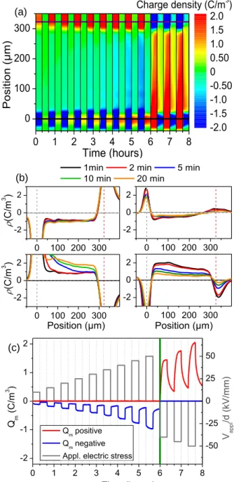
4.2. Space charge in tailored LDPE sample S1 (large isolated AgNPs)
Sample S1, a LDPE tailored with AgNPs/SiOxCy:H nanocomposite stack on one face only (AgNPs of mean size 15 ± 10 nm in diameter), was put into contact with the SC electrode of the PEA system. Figure 7 gives the charge dynamics along the short term protocol. It is strikingly different from the charge dynamics in the reference sample. There is no evidence of positive charge injection from the SC/plasma polymer stack contact up to the end of the polarization period under positive voltage (50 kV/mm). The space charge in the bulk is negative and is due to the migration of the charge injected from the Al/polymer contact. Space charge profiles at 50 kV/mm are shown at different times in Figure 7(b) in polarization and depolarization steps. The presence of negative charge distribution throughout the bulk is confirmed without signs of positive space charge build-up. The AgNPs/SiOxCy:H nanocomposite layer appears efficient to block the formation of positive space charge. Upon polarity reversal, massive space charge formation following injection of positive charge
13
from the contact Al/polymer is evidenced. Contrary to the case of the reference sample, there is no zero net charge domain in the middle of the sample because there is no negative charge injection from the SC/polymer contact. The AgNPs/SiOxCy:H nanocomposite layer appears efficient to block the negative charge injection as well. The representation shown in Figure 7(c) confirms the absence of positive charge formation due to positive injection from the SC/plasma polymer stack. As a consequence the positive charge density after polarity inversion is 4 times higher than in the reference sample.
Figure 7. Space charge dynamics in sample S1 (LDPE tailored with AgNPs/SiOxCy:H nanocomposite stack on
one face only) along the short term protocol: (a) 3D plot of space charge dynamics, (b) charge density profiles during polarization (left) and depolarization (right) for the steps at 50 kV/mm under positive (top) and negative (bottom) applied voltages, and (c) averaged positive and negative charge densities along the protocol.
0 1 2 3 4 5 6 7 8 0 100 200 300 P o sit io n ( µ m ) Time (hours) -2.0 -1.5 -1.0 -0.50 0 0.50 1.0 1.5 2.0 Charge density (C/m3) 0 100 200 300 -2 0 2 0 100 200 300 -2 0 2 (C /m 3 ) Position (µm) (C /m 3 ) 0 100 200 300 -2 0 2 0 100 200 300 -2 0 2 Position (µm) -2 0 2 0100 200 300 -2 0 2
1min 2 min 5 min 10 min 20 min (a) (b) 0 1 2 3 4 5 6 7 8 -2 -1 0 1 2 Q m ( C /m 3 ) Time (hours) Qm positive Qm negative Appl. electric stress
-50 -25 0 25 50 Vappl /d ( kV /m m ) (c)
14
4.3. Space charge in tailored LDPE samples S2 (small isolated AgNPs) and S5 (large coalesced AgNPs)
Tailored LDPE samples S2 and S5 were subsequently tested (AgNPs average sizes <10 nm and 30 nm, respectively) as representatives of small and large average size distribution and organization of the AgNPs, the latter being isolated for S2 and coalesced for S5. Experimental conditions for space charge measurements were otherwise identical to those for S1 sample. The space charge dynamics is shown in Figure 8(a) and 8(b) respectively.
Figure 8. Space charge dynamics in LDPE tailored (with AgNPs/SiOxCy:H nanocomposite stack on one face
only) samples along the short term protocol: (a) S2 (small isolated AgNPs), (b) S5 (large coalesced AgNPs), and (c) S0 (organosilicon matrix only).
0 1 2 3 4 5 6 7 8 0 100 200 300 Time (hours) P o sit io n ( µ m ) -2.0 -1.5 -1.0 -0.50 0 0.50 1.0 1.5 2.0 Charge density (C/m3) (a) 0 1 2 3 4 5 6 7 8 0 100 200 300 Time (hours) P o sit io n ( µ m ) -2.0 -1.5 -1.0 -0.50 0 0.50 1.0 1.5 2.0 Charge density (C/m3) (b) 0 1 2 3 4 5 6 7 8 0 100 200 300 Time (hours) P o sit io n ( µ m ) -2.0 -1.5 -1.0 -0.50 0 0.50 1.0 1.5 2.0 Charge density (C/m3) (c)
15
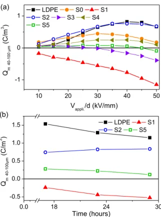
When compared to the space charge distribution in sample S1 (large isolated AgNPs) (Figure 7), one can note a less efficient barrier effect for positive space charge formation, in particular in the case of sample S2 (Figure 8(a)). This conclusion relies on the following analysis. Space charge distribution in sample S2 shows a positive space charge accumulation near the Al cathode during polarization and this accumulation is visible at low electric field (10 kV/mm). Taking into account the analysis of space charge distribution in sample S1, this positive space charge can only be due to a weak injection level at the SC anode followed by a migration of the positive charge towards the cathode where it accumulates and forms a heterocharge layer. The positive space charge density increases with the applied voltage although its spatial extension from the cathode decreases when increasing the voltage. This is due to the negative charge injection from the Al cathode with migration to the SC anode and accumulation nearby as demonstrated by the negative charge build-up near the SC electrode that appears at 40 kV/mm. Overall, both electrodes inject charges and one observes a distribution due to the overlap of the two distributions with heterocharge formation at each electrode. This is typical of situation where the electrodes are partially blocking leading to an unbalance between the incoming charges and the extracted charges at the electrode [28]. The predominance of positive charge near the cathode (at least up to 40 kV/mm) denotes a higher charge injection from the SC anode. A similar analysis can be done in the case of sample S0 (Figure 8(c)) although the positive injection is mitigated when compared to the behavior in sample S1. Heterocharge accumulation following injection and migration of charges of both polarities is also observed although the positive space charge accumulation is less visible, denoting a lower density of positive space charge due to a weaker positive injection. The barrier effect observed in sample S1 (large isolated AgNPs) is therefore also observed in samples S2 (small isolated AgNPs) and S5 (large coalesced AgNPs) but with a lower efficiency, sample S5 having an intermediate behavior between samples S1 and S2. The space charge dynamics and distribution observed after polarity reversal confirm the previous analysis with a higher density of positive charge injected from the Al anode in the case of S5 (which is due to a higher field at the anode when compared to S2). Overall, the integration of the charge density accumulated during polarization under positive voltage between positions 40 m and 100 m from the cathode (arbitrary chosen for rejecting the image charge at the cathode but taking into account the charge density accumulated in its vicinity) can provide a ranking criterion for the barrier effect for charge injection at each voltage level and for each sample type: the higher density of positive charge the higher efficiency for positive charge injection is. When the space charge integrated within the same limits is negative, the barrier effect is all the more efficient that the charge density is high, and is more efficient than when a net positive charge is measured. A plot of the space charge integrated within these limits at each voltage level during polarization is shown in Figure 9(a) for the samples S1, S2 and S5. It confirms a higher efficiency of the barrier effect in sample S1, followed by sample S5 and sample S2.
16
Figure 9. Ranking of the efficiency of the barrier effect to charge injection in each tested sample. Each point represents the space charge integrated over the region 40 µm to 100 µm from the cathode: (a) along the short term protocol during polarization (space charge at the end of each voltage step), and (b) along the longer term protocol at three characteristic times (17, 23 and 28 hours) at 40 kV/mm
5. DISCUSSION
The above reported results raise several questions. Even if an effect of the silver nanoclusters characteristics is observed, one has to discuss the effect of the SiOxCy:H layer by itself. We therefore prepared a LDPE substrate covered with the organosilicon layer without AgNPs (sample S0) in order to investigate the possible effect on charge injection. Another important feature of the results is the apparent barrier effect of the nanocomposite layer on both positive and negative charge injection. To strengthen the analysis, we investigated space charge in a sample tailored on both faces with identical electrodes. Then, the mechanism of charge injection mitigation has to be investigated in order to understand which features of the AgNPs are controlling the charge mitigation. For that purpose, we have performed surface potential measurements on samples with large isolated and coalesced AgNPs. Finally, the barrier effect has to be assessed using a protocol involving longer polarization period (defined as “longer term protocol”).
5.1. Space charge distribution in tailored sample with SiOxCy:H layer.
A sample has been prepared with the deposition of the SiOxCy:H layer on one face and using the same protocol for plasma deposition as in the other tested samples. Thickness and characteristics of the organosilicon layer are the same as for samples containing AgNPs. Figure 8(c) shows the space charge
10 20 30 40 50 -1 0 1 Qm 4 0 -1 0 0 µm ( C /m 3 ) Vappli./d (kV/mm) LDPE S0 S1 S2 S3 S4 S5 (a) 0.0 18 24 30 -0.5 0.0 0.5 1.0 1.5 Qm 4 0 -1 0 0 µm ( C /m 3 ) Time (hours) LDPE S1 S2 S5 (b)
17
dynamics where it can be seen, by comparison with the space charge distribution shown in Figures 6, 7, 8(a) and 8(b) (respectively LDPE reference sample; LDPE tailored samples S1; S2 and S5) that the injection is mitigated in sample S0 when compared to the reference sample but to a lower extent when compared to samples S1 and S5. This is evidenced by the representation of Fig. 9(a) where the integrated charge vs. field plot of sample S0 lies between the curves relative to S5 and S2. It can therefore be concluded that charge injection mitigation is also observed with the organosilicon layer but the barrier effect is greatly enhanced in sample containing AgNPs when the particle size is larger than 10 nm.
5.2. Polarity dependence of the barrier effect on charge injection
In order to investigate precisely this effect, we used a sample tailored on the two faces by AgNPs containing organosilicon layers prepared in the conditions of sample S1 (silver particles having an average size of 15 nm). To avoid the complexity in the analysis of the space charge distribution due to the difference in the nature of the electrodes of the PEA set-up, we used a SC electrode in contact with the Al electrode. The configuration under study is therefore symmetrical with the two faces of the sample being identical in terms of the nature of the contact. Figures 10(a) and 10(b) show the charge distribution dynamics for the LDPE sample and the field distribution at different times during polarization and depolarization. Field enhancement is observed at the cathode for both polarities of the applied voltage due to the fact that the positive space charge originating from injection at the SC anode dominates the space charge distribution. A field intensification of 5.8 kV/mm at the cathode and a field decrease of 8.8 kV/mm at the anode are derived from the space charge distribution at the end of the positive voltage step at 50 kV/mm. It is worth emphasizing small differences between the space charge dynamics of one- and two-faces tailored samples (see respectively Figures 6(a) and 10(a)). This is due to the difference of the contact at the cathode being Al/LDPE and SC/LDPE respectively for one- and two-faces tailored samples. One should note a higher electron injection from the cathode in case of the SC/LDPE contact reducing the net positive charge accumulated near the cathode. Figures 10(c) and 10(d) shows the charge distribution dynamics for the two-faces tailored sample and the field distribution at different times during polarization and depolarization. The barrier effect is clearly revealed at both electrodes without evolution of the electric field distribution. The barrier effect mechanisms are therefore operant for positive and negative charges.
18
Figure 10. Space charge dynamics along the short term protocol and field distribution in polarization and depolarization under different applied voltages: (a) and (b) in reference LDPE sample, and (c) and (d) in two-faces tailored S1 sample (large isolated AgNPs). Note the symmetrical SC/sample contact at anode and cathode.
5.3. Barrier effect and influential features of the Ag NPs
At least three features of the AgNPs have to be considered for interpretation of charge injection mitigation: the average size of the NPs, their surface density and the fact they can be isolated or percolated. Owing to the experimental results, to the least inter-connection and size of particles appear more influential in the range of densities investigated here. The average particles size seems influential with less mitigation effect when it is lower than 10 nm (S2) when compared to 15 nm (S1) or 14 nm (S4). AgNPs in sample S3 (22 nm, isolated clusters) and S5 (30 nm, percolated clusters) have a higher average size and appear also as less efficient in mitigating charge injection than in S1 (15 nm) and S4 (14 nm). It seems therefore that the AgNPs optimum size for charge injection mitigation is about 15 nm. AgNPs in sample S5 are percolated. The electrical properties of a population of NPs in a dielectric matrix change drastically at the percolation threshold [29, 30] where Ag islands form an infinite metallic cluster which spans the whole sample. This can obviously be influential in the mitigation of charge injection. We have investigated the change in electrical properties going from sample S1 (isolated AgNPs) to S5 (percolated AgNPs) by surface potential measurements. The experimental results are shown in Figure 11.
0 1 2 3 4 5 6 7 8 0 100 200 300 Time (hours) P o sit io n ( µ m ) -2.0 -1.5 -1.0 -0.50 0 0.50 1.0 1.5 2.0 Charge density (C/m3) (a) 0 100 200 300 -40 -20 0 20 40 E le ctr ic f ie ld ( kV /m m ) Position (µm) 0 min 20 min Theorical field (b) 0 1 2 3 4 5 6 7 8 0 100 200 300 Time (hours) P o sit io n ( µ m ) -2.0 -1.5 -1.0 -0.50 0 0.50 1.0 1.5 2.0 Charge density (C/m3) (c) (d) 0 100 200 300 -40 -20 0 20 40 E le ctr ic f ie ld ( kV /m m ) Position (µm) 0 min 20 min Theorical field
19
When the AgNPs are percolated (Figure 11(a)), the surface potential appears constant along the scanning lines above the surface of the sample: AgNPs charging is uniform like in a bulk metal and the surface potential decay is rather slow. Percolated AgNPs behave like a metal sheet most probably because charging at one favorable site under the needle leads to charging of the AgNPs belonging to the infinite clusters, i.e. local charging affects the global structure. When the AgNPs are isolated, the surface potential is not uniform along the scanning lines and the surface potential decay is much faster. Charging is inhomogeneous along the sample surface because each cluster has to be charged individually through direct charging by the corona or through lateral conduction from clusters to clusters. This would take time after corona contact and could explain the decay of the surface potential.
Figure 11. Surface potential measurements on (a) S5 (large coalesced AgNPs) and (b) S1 (large isolated AgNPs) samples. Blue lines indicate the edges of the composite layer. Measurements are carried out at different times after charging as indicated.
An efficient mitigation of charge injection appears therefore as a characteristic of isolated AgNPs with a size distribution of the order of 15 nm. The question to be discussed is the cluster size effect observed from sample S1 (AgNPs mean size of 15 nm) to sample S2 (AgNPs mean size is less than 10 nm). Among possible explanation, quantum effects due to the reduction of the number of atoms in the metallic cluster could be evoked. Indeed metal clusters are congregates of atoms that have properties different from both a single atom and the bulk metal. However, as the size of a cluster increases, its properties evolve to those of the bulk. For example, the ionization potential (and electron affinity) of a single atom of Ag will decrease (respectively increase) gradually with an increasing number of silver atoms to reach the metal work function of bulk silver (4.64 eV) [31]. The size dependence of the ionization potentials and electron affinities of metallic clusters varies as R-1, R being the cluster radius [32]. Quantum effects will be stronger for small cluster size and therefore more operant in sample S2 (small isolated AgNPs) when compared to sample S1 (large isolated AgNPs). It is not consistent with experimental data. Another experimental fact is that the charge mitigation by the NPs is observed under both polarities of the applied voltage. Quantum effects due to the size reduction would hardly give an interpretation for the polarity effect. An alternative would be to consider the stability of charged clusters. By using different metal cluster generation and ionization methods, it has been
-20 0 20 0 200 400 600 800 1000 -20 0 20 0 200 400 600 800 1000 S ur fa ce p ote nti al (V ) Longitudinal position (mm) 0min 3min 15min 60min (b) (a)
20
shown that some charged clusters are more stable than others depending on the number of constituting atoms [33]. These so-called “magic numbers” were successfully explained by shell like arrangement of electrons in the cluster, so that the cluster achieves a higher stability at shell closing. Little is known about the stability of multiple charged clusters, even if stable triple charged silver ions (Agn3+) have been observed for specific values of n. In each case, the higher stability was explained by the electronic occupation of shells. Both silver clusters anions [34] and cations [33] have been observed and this could give a basis for the interpretation of the barrier to injection effect observed under both voltage polarities. However, the average size of the Ag clusters in our nanocomposite (estimated to be 3 × 10⁴ atoms and 1 × 10⁵ atoms for 10 nm and 15 nm cluster diameter, respectively) is much higher than the upper limit of a few hundreds of atoms for conventional DFT quantum computation though it might become tractable in the future using developing algorithms [35, 36]. But the possibility that they stabilize positive and negative charge has to be considered. A simple field calculation assuming a single charge state of each cluster in the case of sample S2 leads to a field value at the surface of the electrode adjacent to the charged layer of 63 kV/mm (with a AgNP density of 7.7 × 1011 cm-2, a relative permittivity of 2.2 for LDPE and the distance to the adjacent electrode small in comparison to the total dielectric thickness as is the case in our configuration). Such space-charge induced field is actually of the order of magnitude of the applied field. Besides, if every AgNP accommodates more than one charge, the barrier effect is magnified. A reasonable interpretation of the barrier effect could therefore be a field reduction at the injecting electrode due to AgNPs charging.
5.4. Checking the barrier effect on the longer term
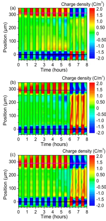
Finally, the mechanism of charge injection mitigation by the presence of AgNPs in the composite layer has to be checked on the longer term. We have used the “longer term protocol” for voltage application as described in paragraph 2.4. The space charge dynamics is shown for reference LDPE, S1, S2 and S5 samples in Figures 12(a), (b), (c) and (d) respectively, for two voltage levels (corresponding fields of 20 and 40 kV/mm) applied for 12 hours each. The criterion defined in paragraph 4.3 was used to compare the barrier effect at three characteristic times during polarization under 40 kV/mm (17, 23, 27 h), for the four samples. Space charge integrated from 40 m to 100 m at these characteristic times has been plotted in Figure 9(b). It can be seen that the barrier effect is still efficient at longer term for sample S1 (large isolated AgNPs covered by an organosilicon thin layer) which strengthens the results obtained with the short term protocol, and the ranking between the different samples is the same as regards the efficiency of the barrier to injection.
21
Figure 12. Space charge dynamics in (a) reference LDPE, (b) S1 (large isolated AgNPs), (c) S2 (small isolated AgNPs), and (d) S5 (large coalesced AgNPs) samples along the longer term protocol.
6. Conclusion
Charge injection from a semi-conducting electrode into low density polyethylene submitted to a DC field has been investigated up to 50 kV/mm through space charge dynamics. A comparison between charge injection efficiency has been achieved when the polyethylene sample was tailored with a SiOxCy:H nanocomposite layer containing a plane of silver nanoparticles having different characteristics. With reference to a polyethylene sample, charge injection mitigation was observed with an increasing intensity upon deposition of the SiOxCy:H layer without AgNPs, with percolated AgNPs and with non-percolated AgNPs of 15 nm. Charge injection is suppressed in the latter case even under high field (50 kV/mm) and the effect is observed for both polarities of the voltage and for longer polarization duration (24 hours). AgNPs appear therefore as a key feature for charge injection suppression. The ability of silver clusters to stabilize electrical charges thereby counterbalancing the injecting field seems to be a key factor in explaining charge injection mitigation.
0 6 12 18 24 30 0 100 200 300 Time (hours) P o sit io n ( µ m ) -2.0 -1.5 -1.0 -0.50 0 0.50 1.0 1.5 2.0 Charge density (C/m3) (a) 0 6 12 18 24 30 0 100 200 300 Time (hours) P o sit io n ( µ m ) -2.0 -1.5 -1.0 -0.50 0 0.50 1.0 1.5 2.0 Charge density (C/m3) (b) 0 6 12 18 24 30 0 100 200 300 Time (hours) P o sit io n ( µ m ) -2.0 -1.5 -1.0 -0.50 0 0.50 1.0 1.5 2.0 Charge density (C/m3) (c) 0 6 12 18 24 30 0 100 200 300 Time (hours) P o sit io n ( µ m ) -2.0 -1.5 -1.0 -0.50 0 0.50 1.0 1.5 2.0 Charge density (C/m3) (d)
22 ACKNOWLEDGMENT
This work was financially supported by the Agence Nationale de la Recherche in France, project ANR-InTail under Contract No. ANR-AA-PBLI-II-2011. The authors acknowledge support from the UMS Raymond Castaing of the University of Toulouse and thank Mr. Stéphane Le Blond du Plouy for the SEM observations.
REFERENCES
[1] Mazzanti G and Marzinotto M 2013 Extruded Cables for High-Voltage Direct-Current Transmission: Advances in Research and Development (Wiley-Blackwell, : New York).
[2] Hanley T L, Burford R P, Fleming R J and Barber K W 2003 A general review of polymeric insulation for use in HVDC cables IEEE Electr. Insul. Mag. 19 13-24.
[3] Khalil M S 1997 International research and development trends and problems of HVDC cables with polymeric insulation IEEE Electr. Insul. Mag. 13 35-47.
[4] Montanari G C and Morshuis P H F 2005 Space charge phenomenology in polymeric insulating materials IEEE Trans. Dielectr. Electr. Insul. 12 754-767.
[5] Laurent C, Teyssedre G, Le Roy S and Boudoin F 2013 Charge dynamics and its energetic features in polymeric materials IEEE Trans. Dielectr. Electr. Insul. 20 357-381.
[6] Less K J and Wilson E G 1973 Intrinsic photoconduction and photoemission in polyethylene J. Phys. C: Solid State Phys. 6 3310-3120.
[7] Thomas C, Teyssedre G and Laurent C 2011 Space-charge dynamic in polyethylene: from dc to ac stress J. Phys. D: Appl. Phys. 44 015401 (8pp).
[8] Fabiani D, Montanari G C, Laurent C, Teyssedre G, Morshuis P H F, Bodega R, Dissado L A, Campus A and Nilsson U H 2007 Polymeric HVDC cable design and space charge accumulation. Part 1 : insulation/semicon interface IEEE Electr. Insul. Mag. 23 11-19.
[9] Taleb M, Teyssèdre G, Le Roy S and Laurent C 2013 Modelling of Charge Injection and Extraction in a Metal/Polymer Interface through an Exponential Distribution of Surface States IEEE Trans. Dielectr. Electr. Insul. 20 311-320.
[10] Vissouvanadin B, Le Roy S, Teyssedre G, Laurent C, Denizet I, Mammeri M and Poisson B 2011 Impact of concentration gradient of polarizable species on the electric field distribution in polymeric insulating material for HVDC cable IEEE Trans. Dielectr. Electr. Insul. 18 958-964.
[11] Tanaka T and Imai T 2013 Advances in nanodielectric materials over the past 50 years IEEE Electr. Insul. Mag. 29 10-23.
[12] Zhao N, Li S, Wang X and Li G 2013 Effects of LDPE/nanofilled LDPE interface on Space Charge Formation IEEE International Conference on Solid Dielectrics (Bologna, Italy) 944-947. [13] Zheng F, Zhang Y, Hao S, Wang W, Xiao C, and An A, 2009 Morphology related packet-like space charge behavior in LLDPE doped with Al2O3 nano-particles J. Appl. Polym. Sci. 112 3103-3109.
23
[14] Liao R, Bai G, Yang L, Cheng H, Yuan Y and Guan J 2013 Improved Electric strength and Space Charge Characterization in LDPE Composites with Montmorillonite Fillers J. Nanomaterials ID 712543 1-7.
[15] Murata Y, Goshowaki M, Reddy C C, Sekiguchi Y, Tanaka Y and Takada T 2008 Investigation of space charge distribution and volume resistivity of XLPE/MgO nanocomposite material under DC voltage application IEEE International Symposium on Electrical Insulating Materials (Yokkaichi, Japan) 502-505.
[16] Nelson J K 2014 Nanodielectrics – the first decade and beyond International Symposium on Electrical insulating Materials, (Niigata City, Japan) 1-11
[17] An Z, Yang Q, Xie C, Jiang Y, Zheng F and Zhang Y 2009 Suppression effect of surface fluorination on charge injection into linear low density polyethylene J. Appl. Phys.105 064102.
[18] Milliere L, Makasheva M, Laurent C, Teyssedre G and Despax B 2014 Silver nanoclusters containing layer as an efficient barrier for charge injection in polyethylene Appl. Phys. Lett. 105, 122908.
[19] Le Roy S, Teyssedre G, Laurent C, Montanari G C and Palmieri F 2006 Description of charge transport in polyethylene using a fluid model with a constant mobility: fitting model and experiments J. Phys. D: Appl. Phys. 39 1427-1436.
[20] Makasheva K, Villeneuve C, Le Roy S, Despax B, Boudou L, Laurent C and Teyssedre G 2013 Silver nanoparticles embedded in dielectric matrix: charge transport analysis with application to control of space charge formation IEEE Conference on Electrical Insulation and Dielectric Phenomena (Shenzhen, China) 238-241, DOI: 10.1109/CEIDP.2013.6747079.
[21] Despax B and Raynaud P 2007 Deposition of polysiloxane thin films containing silver particles
by an RF asymmetrical discharge Plasma Process. Polym. 4 127–134.
[22] Fukunaga K and Maeno T 1997 Internal space charge measurement for the study of the electrostatic phenomena J. Electrostatics 40-41 431-435.
[23] Köhler K, Coburn J W, Horne D E, Keller J H and Kay E 1985 Plasma potentials of 13.56-MHz rf argon glow discharges in a planar system J. Appl. Phys. 57 59-66.
[24] Perrin J, Despax B and Kay E 1985 Optical properties and microstructure of gold–fluorocarbon-polymer composite films Phys. Rev. B 32 719-732.
[25] Laurent C and Kay E 1989 Properties of metal clusters in polymerized hydrocarbon versus fluorocarbon matrices J. Appl. Phys. 65 1717-1723.
[26] Gulmine J V, Janissek P R, Heise H M, and Akcelrud L 2002 Polyethylene characterization by FTIR Polymer Testing 21 557-563.
[27] Xiao C, Zhang Y, An Z, Zheng F, Wei W, and Xuan H 2012 Interface electric field of carbon
black loaded electrode and its significant influence on charge injection into polyethylene J. Appl.
24
[28] Le Roy S, Teyssedre G, Laurent C, Dissado L A and Montanari G C 2007 Relative Importance of Trapping and Extraction in the Simulation of Space Charge Distribution in Polymeric Insulators under DC Potentials International Conference on Solid Dielectric (Winchester, UK) 494-497.
[29] Abeles B, Sheng P, Coutts MD, Arie Y 1975 Structural and electrical properties of granular metal films. Adv. Phys. 24 407–461.
[30] Ping S 1992 Electronic transport in granular metal films Phil. Mag. B 65 357-384.
[31]CRC Handbook on Chemistry and Physics, 89th Revised edition (CRC Press Inc, 2008) 112-114. [32]Harbola M K 1992 Theoretical study of the size dependence of ionization potential and electron affinity of metallic clusters J. Chem. Phys. 97 2578-2582.
[33] Rabin I, Jackschath C and Schulze W 1991 Shell effects in singly and multiply charged silver and gold clusters Z. Phys. D - Atoms, Molecules and Clusters 19 153-155.
[34] Herlerta A, Schweikhard L and Vogel M 2001 Observation of multiply charged silver-cluster anions Eur. Phys. J. D16 65-68.
[35] Hine NDM, Haynes PD, Mostofi AA, Skylaris CK and Payne MC 2009 Linear-scaling density-functional theory with tens of thousands of atoms: Expanding the scope and scale of calculations with ONETEP Computer Phys. Comm. 180 1041-1053
[36] Bowler DR and Miyazaki T 2010 Calculations for millions of atoms with density functional theory: linear scaling shows its potential J. Phys.: Condens. Matter 22 074207