HAL Id: cea-02186164
https://hal-cea.archives-ouvertes.fr/cea-02186164
Submitted on 27 Aug 2019
HAL is a multi-disciplinary open access
archive for the deposit and dissemination of
sci-entific research documents, whether they are
pub-lished or not. The documents may come from
teaching and research institutions in France or
abroad, or from public or private research centers.
L’archive ouverte pluridisciplinaire HAL, est
destinée au dépôt et à la diffusion de documents
scientifiques de niveau recherche, publiés ou non,
émanant des établissements d’enseignement et de
recherche français ou étrangers, des laboratoires
publics ou privés.
Advanced GeSn/SiGeSn Group IV Heterostructure
Lasers
Nils von den Driesch, Daniela Stange, Denis Rainko, Ivan Povstugar, Peter
Zaumseil, Giovanni Capellini, Thomas Schröder, Peter Denneulin, Zoran
Ikonic, Jean-Michel Hartmann, et al.
To cite this version:
Nils von den Driesch, Daniela Stange, Denis Rainko, Ivan Povstugar, Peter Zaumseil, et al.. Advanced
GeSn/SiGeSn Group IV Heterostructure Lasers. Advanced Science, Wiley Open Access, 2018, 5 (6),
pp.1700955. �10.1002/advs.201700955�. �cea-02186164�
www.advancedscience.com
Advanced GeSn/SiGeSn Group IV Heterostructure Lasers
Nils von den Driesch,* Daniela Stange, Denis Rainko, Ivan Povstugar, Peter Zaumseil,
Giovanni Capellini, Thomas Schröder, Thibaud Denneulin, Zoran Ikonic,
Jean-Michel Hartmann, Hans Sigg, Siegfried Mantl, Detlev Grützmacher, and Dan Buca*
DOI: 10.1002/advs.201700955
The ever-increasing demand for computational power, e.g., in data centers or consumer electronics, requires new approaches tackling energy efficiency of computer chips. Optical short-range and on-chip communication may here offer dramati-cally reduced power dissipation.[1] In this respect, Group
Growth and characterization of advanced group IV semiconductor materials with CMOS-compatible applications are demonstrated, both in photonics. The investigated GeSn/SiGeSn heterostructures combine direct bandgap GeSn active layers with indirect gap ternary SiGeSn claddings, a design proven its worth already decades ago in the III–V material system. Different types of double heterostructures and multi-quantum wells (MQWs) are epitaxially grown with varying well thicknesses and barriers. The retaining high material quality of those complex structures is probed by advanced characterization methods, such as atom probe tomography and dark-field electron holography to extract composition parameters and strain, used further for band structure calculations. Special emphasis is put on the impact of carrier confinement and quantization effects, evaluated by photoluminescence and validated by theoretical calcula-tions. As shown, particularly MQW heterostructures promise the highest poten-tial for efficient next generation complementary metal-oxide-semiconductor (CMOS)-compatible group IV lasers.
Lasers
Dr. N. von den Driesch, D. Stange, D. Rainko, Prof. S. Mantl, Prof. D. Grützmacher, Dr. D. Buca
Peter Grünberg Institute 9 (PGI-9) and JARA-Fundamentals of Future Information Technologies (JARA-FIT)
Forschungszentrum Jülich, 52425 Jülich, Germany
E-mail: [email protected]; [email protected] Dr. I. Povstugar
Central Institute for Engineering, Electronics and Analytics Forschungszentrum Jülich, 52425 Jülich, Germany Dr. P. Zaumseil, Prof. G. Capellini, Prof. T. Schröder IHP
15236 Frankfurt (Oder), Germany Prof. G. Capellini
Department of Sciences Università Roma Tre 00154 Rome, Italy
The ORCID identification number(s) for the author(s) of this article can be found under https://doi.org/10.1002/advs.201700955.
Dr. T. Denneulin CEMES CNRS
31055 Toulouse, France Dr. T. Denneulin
Ernst Ruska-Centre for Microscopy and Spectroscopy with Electrons and Peter Grünberg Institute 5 (PGI-5)
Forschungszentrum Jülich, 52425 Jülich, Germany Dr. Z. Ikonic
Institute of Microwaves and Photonics School of Electronic and Electrical Engineering University of Leeds Leeds LS2 9JT, UK Dr. J.-M. Hartmann CEA LETI MINATEC Campus F-38054 Grenoble, France Dr. J.-M. Hartmann Université Grenoble Alpes F-38000 Grenoble, France Dr. H. Sigg
Laboratory for Micro- and Nanotechnology (LMN) Paul Scherrer Institute
CH -5232 Villigen, Switzerland
IV photonics is the key technology,[2,3]
allowing seamless integration of com-plementary metal-oxide-semiconductor (CMOS)-based electronics with optical components.[4,5] Since the indirect nature
of their bandgap hinders Si and Ge from acting as efficient light emitters, heteroge-neous integration[6] and epitaxy of III–V
materials on Si are the solutions presently investigated, yielding optically[7] and
elec-trically driven[8,9] lasers. Recently,
solu-tions based on pure group IV alloys got renewed interest as incorporation of group IV element tin (Sn) in Ge and SiGe has led to (i) the formation of truly Si-compatible, direct gap GeSn[10] and SiGeSn[11] systems
and, (ii) several demonstrations of GeSn optically pumped lasing.[10,12–14] Moreover,
their bandgap in the mid-infrared range turns them into key materials for biolog-ical and chembiolog-ical sensing applications.[3]
Electrically induced luminescence has been, however, so far demonstrated only for homojunction diodes and/or for indirect gap GeSn structures.[15–18]
Lessons learned from highly mature III–V laser materials can serve as a model for developing more efficient group IV
© 2018 The Authors. Published by WILEY-VCH Verlag GmbH & Co. KGaA, Weinheim. This is an open access article under the terms of the Creative Commons Attribution License, which permits use, distribution and re-production in any medium, provided the original work is properly cited.
www.advancedsciencenews.com www.advancedscience.com
light emitters, e.g., by introduction of heterostructures or uti-lizing quantum size effects in the active region.[19] In this
respect, larger-bandgap SiGeSn ternaries appear to be natural candidates for heterostructures.[20,21] The use of Sn-based
het-erostructures and quantum wells combining binaries and ternaries has been theoretically proposed for energy efficient electronic devices,[22] photonic applications,[20,21] or
photo-voltaics.[23] Epitaxial growth and characterization were, however,
mostly limited to bulk layers[11,24,25] or single wells.[26] Recently,
its epitaxial integration for GeSn/SiGeSn heterostructure light emitting diodes (LEDs) has been demonstrated,[11] which
sig-nificantly improved emission characteristics compared to bulk homojunction LEDs.[27] However, no combination of SiGeSn
with direct bandgap GeSn has been demonstrated yet, which will be the key for any efficient light emitter.
In the present study, we report on growth and characteriza-tion of various types of GeSn/SiGeSn heterostructures, com-bining for the first time relaxed direct bandgap GeSn active layers with SiGeSn barriers. Based on our theoretical models and experimental photoluminescence (PL) and lasing data, the presented work gives a promising perspective for group IV het-erostructure lasers, paving the way toward integrated emitters on Si platform.
The heterostructures investigated here make use of buffer technology. A partially relaxed 200 nm thick lower Sn content Ge0.9Sn0.1 layer is used as buffer. It reduces the lattice
mis-match between the Ge virtual substrate (Ge-VS) underneath and the top Ge1−xSnx active layer, allowing higher Sn
incorpo-ration (x > 10%) and diminished compressive strain. As those properties increase the energy difference between the indirect L- and the direct Γ-valley, later termed directness, emission properties shall be strongly enhanced in the active region.[28]
The first investigated heterostructure type are double hetero-structures (DHSs), where a highly strain relaxed GeSn active layer with high Sn incorporation of about 14 at%, sandwiched between two SiGeSn barrier layers, is targeted. A straightfor-ward way to increase Sn incorporation in GeSn alloys, while maintaining high layer quality, is to decrease growth temper-ature.[29] This, on the other hand, limits the amount of
incor-porable Si in the SiGeSn cladding layers due to the limited disilane precursor cracking.[11] Large amount of Si
incorpora-tion is, however, required for high band offsets to the active region. Moreover, due to the metastable nature of Sn-based alloys, optimizing the thermal budget during growth is utterly important.[30,31] Therefore, growth methodology is crucial.
Two different approaches were used for the DHS stacks (see
Table 1). For the first one, consequently labeled DHS1, the
GeSn buffer and bottom SiGeSn cladding were grown in one step at a temperature of 360 °C. Then, the reactor was cooled to 350 °C for growth of the active GeSn region and the top SiGeSn cladding layer. For the second structure, labeled DHS2, the temperature reduction occurred directly after buffer growth, so that the complete SiGeSn/GeSn/SiGeSn DHS stack was grown at 350 °C. Thus, the main difference between the two structures is the stoichiometry of the bottom SiGeSn layers, which was extracted to a Si/Sn incorporation of 5.5/11.5 and 5.5/13 at% for DHS 1 and DHS2, respectively. Details can be found in the Experimental Section and Table 1. For DHS1, this difference leads to better carrier confinement both for L- and especially for Γ-electrons (110 meV for DHS1 vs 47 meV DHS2), which is shown later in Figure 3a.
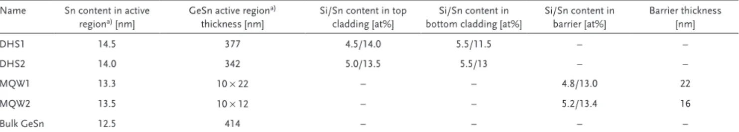
X-ray diffraction reciprocal space maps (XRD-RSMs) indicate that the Ge0.9Sn0.1 buffers are partly relaxed with a residual
com-pressive strain of only −0.4% (shown for DHS1 in Figure 1a). Both cladding layers are, if at all, hardly distinguishable in the RSM. The bottom SiGeSn cladding layer’s signal largely super-imposes the one from the GeSn buffer. The top SiGeSn layer is grown coherently on top of the active GeSn, and can be linked to a signal with the same in-plane reciprocal lattice constant
Qx (see Figure 1a). The active Ge0.855Sn0.145 layer in DHS1 and
Ge0.86Sn0.14 layer in DHS2 are partly relaxed with respect to the
Ge0.90Sn0.10 buffers, being under compressive strain of −0.56%
and −0.70%, respectively. Transmission electron microscopy (TEM) analysis (Figure 1b) indicates the formation of additional unwanted misfit dislocations at the bottom SiGeSn/active GeSn interface, some of which are marked by white arrows. Apart from that, very homogeneous incorporation of Sn atoms throughout the structure is evidenced by the overlaid secondary ion mass spectrometry (SIMS) depth profile, showing that Si atoms are present only in the cladding regions.
Microdisk lasers were fabricated according to the procedure reported in ref. [12] to study the influence of confinement and
misfit dislocations on lasing characteristics, such as threshold and maximum operating temperature. Both the heterostruc-tures show lasing under 1550 nm wavelength optical pumping at 20 K, as depicted in Figure 1c,d in comparison to PL. The dif-ference in PL emission wavelength of both the structures can be attributed to small Sn variations, while the shift of lasing emission is a consequence of both band filling (blueshift) and layer relaxation in underetched microdisks (redshift).
Table 1. Overview on the main structural properties of the grown heterostructures. Except for the bulk GeSn layer, all heterostructure samples feature
a 200 nm thick partially relaxed Ge0.9Sn0.1 buffer.
Name Sn content in active regiona) [nm]
GeSn active regiona)
thickness [nm]
Si/Sn content in top cladding [at%]
Si/Sn content in bottom cladding [at%]
Si/Sn content in barrier [at%] Barrier thickness [nm] DHS1 14.5 377 4.5/14.0 5.5/11.5 – – DHS2 14.0 342 5.0/13.5 5.5/13 – – MQW1 13.3 10 × 22 – – 4.8/13.0 22 MQW2 13.5 10 × 12 – – 5.2/13.4 16 Bulk GeSn 12.5 414 – – – –
This first demonstration of optically pumped lasing in group IV heterostructures discloses two important findings. First and foremost, lasing is achieved with SiGeSn ternaries as barriers to form heterostructures. As shown in Figure 1e, however, lasing ceases at temperatures above 120 K, where the linearity of the light-in light-out (LL) curve throughout all pumping levels can be taken as a sign of spontaneous emission domi-nated luminescence. This is linked to increased losses from nonradiative recombination through defects or Γ–L intervalley scattering, which cannot be overcome by the material gain anymore.
In comparison to laser structures reported earlier in litera-ture,[12,14] introduction of different SiGeSn claddings for carrier
confinement does not result in improved lasing thresholds. Their theoretical advantage seems to be shadowed by a common drawback of both structures: a newly formed misfit dislocation network at the GeSn/SiGeSn interface, making the structures behave similar to bulk GeSn layers. This major drawback can be overcome by using strain-adjusted heterostructures, such as
GeSn/SiGeSn multi-quantum wells (MQWs), as we show in the following text.
Two such heterostructures, MQW1 and MQW2 (see Table 1), each containing ten periods of GeSn wells and SiGeSn barriers, were grown on top of a partially relaxed Ge0.9Sn0.1 buffer, similar to the DHS samples. XRD and
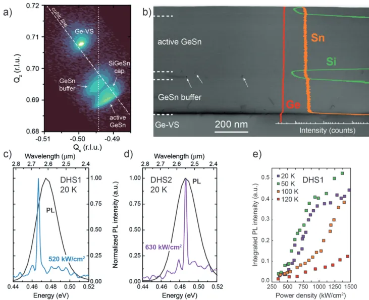
depth-calibrated SIMS measurements (not shown here) yield well thicknesses of 22 and 12 nm, respectively. Due to the complexity of the MQW stack, XRD measurements can deliver only average compositional information of the sulattices. Instead, high resolution elemental analysis was per-formed by means of atom probe tomography (APT). The reconstructed Si atom positions for MQW1 are shown in
Figure 2a. Si atoms are strictly confined within the SiGeSn
barriers, with only 0.03 at% found in the well region. Ele-mental profiles (Figure 2b) passing across six central wells, indicate a Sn content of 13.3 at% in the wells, while Si and Sn incorporation of 4.8 and 13.0 at%, respectively, are extracted for the SiGeSn barriers.
Figure 1. a) XRD-RSM of DHS (DHS1). b) Cross-sectional TEM image of a SiGeSn/GeSn/SiGeSn DHS (DHS2), the different layers can be distinguished
www.advancedsciencenews.com www.advancedscience.com
The distinct advantage of the MQW structure is revealed by dark-field electron holography measurements (MQW2 shown here). Due to its high spatial resolution of about 6 nm, in- and out-of-plane deformations can be locally resolved. Colored lat-tice deformation maps reflect latlat-tice strain differences for out-of-plane (Figure 2c) and in-plane (Figure 2d) directions. The constant in-plane deformation, obvious in the line scans through buffer and MQW in Figure 2e, proves coherent growth of the MQW on top of the Ge0.9Sn0.1 buffer. This should
greatly enhance light emission, as the nonradiative recombina-tion of carriers at the bottom interface with the buffer can be eliminated.[32]
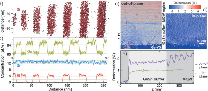
In Figure 3a–c, the calculated conduction band energies in DHS1, DHS2, MQW1, and MQW2 heterostructures are shown. Solid lines represent the lowest bulk conduction band energy, and dotted lines denote the first quantized electron state at Γ. For easier comparison, the displayed conduction band and state energies are measured from the top valence band energy, which in case of the MQW structures is the first quantized heavy hole state. Normalized low temperature PL is juxta-posed in Figure 3d–f to illustrate the effect of quantum con-finement in the Ge0.867Sn0.133 wells. For DHS2, the predicted
bandgap of 0.474 eV closely fits PL emission at about 0.485 eV. A large blueshift of PL emission for the MQW heterostructure with 22 nm well thickness can be observed Figure 3e, which is attributed to a slightly smaller Sn incorporation (13.3 at% instead of 14 at% Sn) and to level splitting because of quantiza-tion. The additional blueshift of 20 meV for the MQW2 sample with 12 nm thin wells (Figure 3f) is solely a quantum confine-ment effect, as indicated by band structure calculations. Thus, clear emission from quantized states is observed in the MQW heterostructures.
Temperature-dependent PL emission between 4 K and room temperature offers additional information on carrier confine-ment. As shown in Figure 4a,b, DHS1 shows only a margin-ally increased PL signal at cryogenic temperatures compared to
a 400 nm bulk GeSn layer with 12.5 at% Sn. A different pic-ture emerges for the 22 nm MQW heterostrucpic-ture (MQW1) in Figure 4c. Coherent growth leads to a strong increase of PL at low temperatures (an order of magnitude at 4 K). This distinct advantage is expected to result from both the confinement of carriers in the GeSn wells and their spatial separation from the GeSn/Ge–VS defective interface. Such a heterostructure is expected to improve lasing performance, such as the lasing threshold, which will be discussed in more details elsewhere. However, too strong quantization, as present in MQW2, dimin-ishes the energy difference between Γ- and L-valleys due to the smaller effective mass of Γ-electrons in comparison to L.[16]
In this case, the decreased directness (and even transition to indirect semiconductor for thinnest wells) leads to poor light emission (98% less PL emission at 4 K compared to MQW1).
The above described PL effects are quantified in a loga-rithmic plot of the integrated PL intensity in Figure 4d. The first observation is that DHS1 yields no light emission improve-ment over a bulk GeSn sample (see Table 1), as both are limited by the above mentioned misfit dislocation network at the GeSn/ SiGeSn interface. In contrast, MQW1 shows the strongest PL emission of the investigated samples, at least at cryogenic temperatures, hinting to a considerably increased nonradia-tive lifetime. The particular advantage of MQW1 in terms of light emission, however, disappears for temperatures above ≈150 K. This can be related to the relatively low conduction band offset between wells and barriers (13 meV determined by band structure calculations). Above this temperature, car-riers are able to overcome the energetic barcar-riers and nonradia-tive recombination at the GeSn/Ge interface sets in. In fact, at room temperature, the integrated MQW1 PL emission intensity is below the one of DHS1 and the bulk GeSn sample, which we attribute to the thinner optically active layers. Therefore, we can deduce that coherent growth, i.e., epitaxy schemes avoiding the formation of additional misfit dislocations, is the most vital pathway toward further improvement of the optical properties.
Figure 2. a) Si elemental map and b) concentration profiles across wells and barriers from atom probe tomography analysis of a GeSn/SiGeSn MQW
Figure 4. Temperature-dependent PL emission for a) bulk GeSn, b) a double heterostructure, and c) a multi-quantum well with 22 nm well thickness.
d) Integrated PL intensity shows the strongest emission from MQW1 at cryogenic temperatures.
Figure 3. Conduction band alignment (and the lowest quantized states positions) for a) DHS1 and DHS2 and MQW samples with b) 22 nm well
www.advancedsciencenews.com www.advancedscience.com
For example, growth of thinner active regions and/or optimized GeSn buffers will be developed. Moreover, to effectively screen carriers from nonradiative recombination sinks at the bottom GeSn/Ge interface, we consider growing SiGeSn barriers with higher Si content. In that case, we expect a distinct advantage of MQW heterostructures, compared to double heterostructures and even more bulk GeSn layers. These features may allow room temperature, low threshold lasers made entirely from group IV materials.
In summary, we demonstrated the potential of group IV epitaxy for the fabrication of direct bandgap heterostructures. Different designs, from bulk to double heterostructures and multi-quantum wells, were epitaxially grown and character-ized. A high sample quality is proven by the first demonstra-tion of optically pumped lasing from group IV GeSn/SiGeSn heterostructures. For the MQW heterostructures, a shift in light emission is achieved by controlling the quantum confinement of carriers through varying well thicknesses. But most impor-tantly, this type of structure outperforms double heterostruc-tures, because of the spatial separation of misfit dislocations from the active region. We indicated that by increasing the het-erostructure barriers, the favorable MQW emission properties can be extended to higher temperatures, possibly up to room temperature. In conclusion, we believe that, as demonstrated decades ago already for the III–V material system, group IV heterostructures and multi-quantum wells are potential ena-blers for high efficient integrated light emitters.
Experimental Section
Epitaxy: All investigated layers were produced by means of chemical
vapor deposition (CVD) in an industry-compatible reactor design on 200 mm wafers. The employed precursors disilane (Si2H6), digermane
(Ge2H6), and tin tetrachloride (SnCl4) ensure high growth rates (typically
15–20 nm min−1) at low growth temperatures (between 350 and 360 °C), helpful for suppression of quality-degrading Sn precipitates and surface segregation. To reduce the large lattice mismatch between the Si (001) and the (Si)GeSn alloys, growth was performed on top of around 2.5 µm thick Ge–VS.[33] Prior to the growth, the native oxide was removed in
an automated single-wafer cleaning tool using hydrofluoric acid vapor chemistry, followed by an in situ hydrogen bake.
Material Characterization: The local material parameters inside
the complex heterostructures were determined by a large number of techniques. For the MQWs, exact compositions were obtained using APT, while energy-dispersive X-ray spectroscopy (EDX) mapping ensured precise values for the DHS. Layer thicknesses were determined likewise from EDX and validated from XRD (MQW) and SIMS (DHS). Strain values were obtained from XRD reciprocal space maps and validated by dark-field electron holography maps.
Band structure values at critical energies were obtained at 0 K by the empirical pseudopotential method and appropriate strain correction within an 8-band k∙p framework. The effect of temperature was included via Varshni’s empirical relations. All theoretical parameters, required for modeling the band structure, can be found in ref. [27] and the Supporting Information of ref. [10].
Acknowledgements
This research received funding for CVD growth investigations from the Federal Ministry of Education and Research (BMBF) under project UltraLowPow (16ES0060 K). The authors further acknowledge
financial support by the BMBF in frame of the M-ERA.NET project GESNAPHOTO, support by the German Research Foundation (DFG) through the project SiGeSn Laser for Silicon Photonics, and from The Royal Society International Exchanges grant IE131593.
Conflict of Interest
The authors declare no conflict of interest.
Keywords
GeSn, heterostructures, lasers, multi-quantum wells, SiGeSn
Received: December 1, 2017 Revised: February 25, 2018 Published online: March 27, 2018
[1] D. A. B. Miller, Proc. IEEE 2000, 88, 728.
[2] R. Soref, D. Buca, S.-Q. Yu, Opt. Photonics News 2016, 27, 32. [3] R. Soref, Nat. Photonics 2010, 4, 495.
[4] J. J. Ackert, D. J. Thomson, L. Shen, A. C. Peacock, P. E. Jessop, G. T. Reed, G. Z. Mashanovich, A. P. Knights, Nat. Photonics 2015,
9, 393.
[5] C. Sun, M. T. Wade, Y. Lee, J. S. Orcutt, L. Alloatti, M. S. Georgas, A. S. Waterman, J. M. Shainline, R. R. Avizienis, S. Lin, B. R. Moss, R. Kumar, F. Pavanello, A. H. Atabaki, H. M. Cook, A. J. Ou, J. C. Leu, Y.-H. Chen, K. Asanović, R. J. Ram, M. A. Popovic´, V. M. Stojanovic´, Nature 2015, 528, 534.
[6] G. Morthier, G. Roelkens, D. Van Thourhout, in Compact
Semicon-ductor Lasers (Eds: R. DeLa Rue, J.-M. Lourtioz, S. Yu), Wiley-VCH
Verlag GmbH & Co. KGaA, Weinheim, Germany 2014, pp. 195–230. [7] B. Tian, Z. Wang, M. Pantouvaki, P. Absil, J. Van Campenhout,
C. Merckling, D. Van Thourhout, Nano Lett. 2017, 17, 559.
[8] Y. Sun, K. Zhou, Q. Sun, J. Liu, M. Feng, Z. Li, Y. Zhou, L. Zhang, D. Li, S. Zhang, M. Ikeda, S. Liu, H. Yang, Nat. Photonics 2016, 10, 595.
[9] S. Chen, W. Li, J. Wu, Q. Jiang, M. Tang, S. Shutts, S. N. Elliott, A. Sobiesierski, A. J. Seeds, I. Ross, P. M. Smowton, H. Liu, Nat.
Photonics 2016, 10, 307.
[10] S. Wirths, R. Geiger, N. von den Driesch, G. Mussler, T. Stoica, S. Mantl, Z. Ikonić, M. Luysberg, S. Chiussi, J.-M. Hartmann, H. Sigg, J. Faist, D. Buca, D. Grützmacher, Nat. Photonics 2015, 9, 88.
[11] N. von den Driesch, D. Stange, S. Wirths, D. Rainko, I. Povstugar, A. Savenko, U. Breuer, R. Geiger, H. Sigg, Z. Ikonić, J.-M. Hartmann, D. Grützmacher, S. Mantl, D. Buca, Small 2017, 13, 1603321. [12] D. Stange, S. Wirths, R. Geiger, C. Schulte-Braucks, B. Marzban,
N. von den Driesch, G. Mussler, T. Zabel, T. Stoica, J.-M. Hartmann, S. Mantl, Z. Ikonić, D. Grützmacher, H. Sigg, J. Witzens, D. Buca,
ACS Photonics 2016, 3, 1279.
[13] V. Reboud, A. Gassenq, N. Pauc, J. Aubin, L. Milord, Q. M. Thai, M. Bertrand, K. Guilloy, D. Rouchon, J. Rothman, T. Zabel, F. Armand Pilon, H. Sigg, A. Chelnokov, J. M. Hartmann, V. Calvo,
Appl. Phys. Lett. 2017, 111, 92101.
[14] J. Margetis, S. Al-Kabi, W. Du, W. Dou, Y. Zhou, T. Pham, P. Grant, S. Ghetmiri, A. Mosleh, B. Li, J. Liu, G. Sun, R. Soref, J. Tolle, M. Mortazavi, S.-Q. Yu, ACS Photonics 2017, https://doi. org/10.1021/acsphotonics.7b00938.
[15] J. D. Gallagher, C. L. Senaratne, C. Xu, P. Sims, T. Aoki, D. J. Smith, J. Menéndez, J. Kouvetakis, J. Appl. Phys. 2015, 117, 245704.
[16] D. Stange, N. von den Driesch, D. Rainko, C. Schulte-Braucks, S. Wirths, G. Mussler, A. T. Tiedemann, T. Stoica, J.-M. Hartmann, Z. Ikonic´, S. Mantl, D. Grützmacher, D. Buca, Opt. Express 2016, 24, 1358.
[17] B. Schwartz, M. Oehme, K. Kostecki, D. Widmann, M. Gollhofer, R. Koerner, S. Bechler, I. A. Fischer, T. Wendav, E. Kasper, J. Schulze, M. Kittler, Opt. Lett. 2015, 40, 3209.
[18] Y. Zhou, W. Dou, W. Du, T. Pham, S. A. Ghetmiri, S. Al-Kabi, A. Mosleh, M. Alher, J. Margetis, J. Tolle, G. Sun, R. Soref, B. Li, M. Mortazavi, H. Naseem, S.-Q. Yu, J. Appl. Phys. 2016, 120, 23102.
[19] Z. Alferov, IEEE J. Sel. Top. Quantum Electron. 2000, 6, 832. [20] G. Sun, R. A. Soref, H. H. Cheng, Opt. Express 2010, 18, 19957. [21] P. Moontragoon, R. A. Soref, Z. Ikonic´, J. Appl. Phys. 2012, 112,
73106.
[22] S. Wirths, A. T. Tiedemann, Z. Ikonic´, P. Harrison, B. Holländer, T. Stoica, G. Mussler, M. Myronov, J.-M. Hartmann, D. Grützmacher, D. Buca, S. Mantl, Appl. Phys. Lett. 2013, 102, 192103.
[23] A. Attiaoui, S. Wirths, A.-P. Blanchard-Dionne, M. Meunier, J. M. Hartmann, D. Buca, O. Moutanabbir, arXiv ID: 1702.00682
2017.
[24] C. Xu, R. T. Beeler, L. Jiang, J. D. Gallagher, R. Favaro, J. Menéndez, J. Kouvetakis, Thin Solid Films 2014, 557, 177.
[25] S. Wirths, D. Buca, Z. Ikonic´, P. Harrison, A. T. Tiedemann, B. Holländer, T. Stoica, G. Mussler, U. Breuer, J.-M. Hartmann, D. Grützmacher, S. Mantl, Thin Solid Films 2014, 557, 183.
[26] S. A. Ghetmiri, Y. Zhou, J. Margetis, S. Al-Kabi, W. Dou, A. Mosleh, W. Du, A. Kuchuk, J. Liu, G. Sun, R. A. Soref, J. Tolle, H. A. Naseem, B. Li, M. Mortazavi, S.-Q. Yu, Opt. Lett. 2017, 42, 387.
[27] D. Stange, N. von den Driesch, D. Rainko, S. Roesgaard, I. Povstugar, J.-M. Hartmann, T. Stoica, Z. Ikonic´, S. Mantl, D. Grützmacher, D. Buca, Optica 2017, 4, 185.
[28] D. Stange, S. Wirths, N. von den Driesch, G. Mussler, T. Stoica, Z. Ikonic´, J. M. Hartmann, S. Mantl, D. Grützmacher, D. Buca, ACS
Photonics 2015, 2, 1539.
[29] N. von den Driesch, D. Stange, S. Wirths, G. Mussler, B. Holländer, Z. Ikonic´, J. M. Hartmann, T. Stoica, S. Mantl, D. Grützmacher, D. Buca, Chem. Mater. 2015, 27, 4693.
[30] R. Chen, Y.-C. Huang, S. Gupta, A. C. Lin, E. Sanchez, Y. Kim, K. C. Saraswat, T. I. Kamins, J. S. Harris, J. Cryst. Growth 2013, 365, 29. [31] S. Takeuchi, A. Sakai, O. Nakatsuka, M. Ogawa, S. Zaima, Thin
Solid Films 2008, 517, 159.
[32] F. Pezzoli, A. Giorgioni, D. Patchett, M. Myronov, ACS Photonics
2016, 3, 2004.
[33] J. M. Hartmann, A. Abbadie, N. Cherkashin, H. Grampeix, L. Clavelier, Semicond. Sci. Technol. 2009, 24, 55002.