Tunable
2D binary colloidal alloys for soft
nanotemplating
†
Miguel Ángel Fernández-Rodríguez,
‡
aRoey Elnathan,
‡
bRan Ditcovski,
cFabio Grillo,
aGaurasundar Marc Conley,
dFlavia Timpu,
eAstrid Rauh,
fKaren Geisel,
gTal Ellenbogen,
cRachel Grange,
eFrank Sche
ffold,
dMatthias Karg,
fWalter Richtering,
gNicolas H. Voelcker
b,h,iand Lucio Isa
*
aThe realization of non-close-packed nanoscale patterns with multiple feature sizes and length scales via colloidal self-assembly is a highly challenging task. We demonstrate here the creation of a variety of tunable particle arrays by harnessing the sequential self-assembly and deposition of two differently sized microgel particles at the fluid–fluid interface. The two-step process is essential to achieve a library of 2D binary colloidal alloys, which are kinetically inaccessible by direct co-assembly. These versatile binary patterns can be exploited for a range of end-uses. Here we show that they can for instance be transferred to silicon substrates, where they act as masks for the metal-assisted chemical etching of binary arrays of vertically aligned silicon nanowires (VA-SiNWs) withfine geo-metrical control. In particular, continuous binary gradients in both NW spacing and height can be achieved. Notably, these binary VA-SiNW platforms exhibit interesting anti-reflective properties in the visible range, in agreement with simulations. The proposed strategy can also be used for the precise placement of metallic nanoparticles in non-close-packed arrays. Sequential depositions of soft particles enable therefore the exploration of complex
binary patterns, e.g. for the future development of substrates for biointerfaces, catalysis and controlled wetting.
Crystalline monolayers from binary mixtures of colloidal par-ticles (2D colloidal alloys) freely floating at a fluid–fluid inter-face constitute ideal model systems to study the structure and
dynamics of materials,1–6but they become even more
interest-ing for applications after they are transferred onto solid
sup-ports.7For instance, they can be used as photonic crystals with
combined band gaps,8 to produce superhydrophobic surfaces
thanks to their hierarchical features,9 to realize plasmonic
materials when noble-metal particles are used,10 or for
enhanced electronic properties when semiconducting ones are
employed.11Additionally, versatile binary patterns can also be
highly beneficial for the realization of vertically aligned silicon
nanowire arrays (VA-SiNWs) for catalysis,12 energy conversion
and storage,13and to engineer nano-bio cellular interfaces.14–16
For both fundamental studies and applications, full control on the particle size, separation and arrangement is highly desirable. Nevertheless, practically all fabrication strategies for 2D binary colloidal alloys present a major constraint: all the particles are in direct contact after deposition on the solid sub-strate. As a consequence, the interparticle distance cannot be independently and continuously changed relative to the par-ticle size, especially over the same substrate. This is the case for both one-step methods, e.g. where binary particle popu-lations are co-injected and deposited from a fluid
inter-face,17,18 or two-step methods, where particles of different
sizes or material are deposited onto a substrate one after the other, e.g. by spin-coating, dip-coating or capillary
assembly.8,9,19,20 In these cases, typical structures display
compact arrays of the larger colloids with the small particles in the interstices. A range of strategies has been proposed to achieve non-close-packed single-component crystalline
monolayers,21–26but the possibilities to produce tunable,
non-close-packed binary arrays remains practically untapped. We report here a two-step method for the fabrication of tunable 2D binary colloidal alloys based on sequential
†Electronic supplementary information (ESI) available. See DOI: 10.1039/ c8nr07059h
‡These authors contributed equally to this work.
aLaboratory for Interfaces, Soft matter and Assembly, Department of Materials, ETH Zurich, 8093 Zurich, Switzerland. E-mail: [email protected] bDrug Delivery, Disposition and Dynamics, Monash Institute of Pharmaceutical Sciences Monash University, 381 Royal Parade, Parkville, Victoria, 3052, Australia cDepartment of Physical Electronics, School of Electrical Engineering,
Tel Aviv University, Tel Aviv-Yafo, Israel
dDepartment of Physics, University of Fribourg, CH-1700 Fribourg, Switzerland eInstitute for Quantum Electronics, Department of Physics, ETH Zurich, 8093 Zurich, Switzerland
fPhysical Chemistry I, Heinrich-Heine-University Duesseldorf, 40204 Duesseldorf, Germany
gPhysical Chemistry II, RWTH Aachen University, 52062 Aachen, Germany hMelbourne Centre for Nanofabrication, Victorian Node of the Australian National Fabrication Facility, 151 Wellington Road, Clayton, Victoria, 3168, Australia iINM-Leibniz Institute for New Materials, Campus D2 2, Saarbrücken, 66123, Germany
http://doc.rero.ch
depositions of Langmuir monolayers of soft core–shell
poly(N-iso-propylacrylamide) (PNIPAM) microgels of different sizes
onto a silicon substrate. By simultaneously compressing a par-ticle-laden water/hexane interface and lifting a silicon wafer through it, we fabricate complex microgel binary arrays, achiev-ing independent control on the size and separation of each particle type. We furthermore demonstrate the process using a
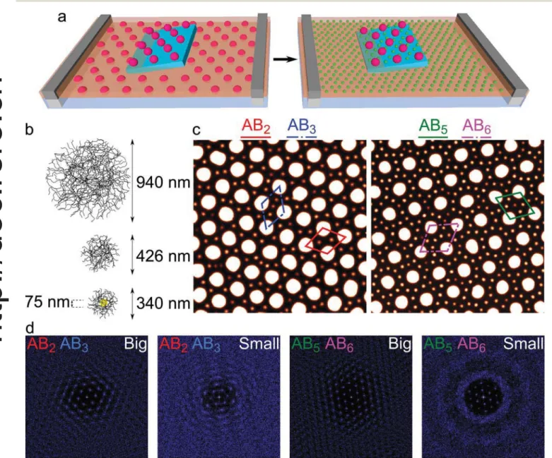
variety of different soft microgel-based nanoparticles (Fig. 1a,
and Fig. S1 in the ESI†). In particular, we use two differently
sized PNIPAM microgels with bulk hydrodynamic diameters of
940 nm and 426 nm, hereon termed‘big’ and ‘small’
micro-gels, and core–shell nanoparticles with a gold core of 75 nm
embedded in a PNIPAM shell with a bulk hydrodynamic
dia-meter of 340 nm, hereon termed ‘gold core–shell’ particles
(Fig. 1b).
One-step routes, i.e. pre-mixing the big and small microgels before confining them at the water/hexane interface or simul-taneously co-injecting them at the interface from two separate syringes, do not lead to the realization of uniform binary
lattices (Fig. S2 and S3 in the ESI†). In both cases, the big
Fig. 1 (a) Scheme of the sequential deposition technique at the water/hexane interface:first (left scheme), the big microgels are deposited from the interface by lifting the silicon substrate and controlling the interfacial pressureΠbigusing the barriers of the Langmuir trough. In a second step
(right scheme), the same substrate is immersed in water and a second layer of small microgels is deposited from the interface, with controlledΠsmall.
(b) Scheme of the three types of soft core–shell PNIPAM microgels used in this study: big, small and gold core–shell particles. (c) AFM images (10 × 10μm2) showing different microstructures of deposited binary arrays with varying interparticle distances between the big and small microgels (left:
Πbig= 4 mN m−1andΠsmall= 5 mN m−1, right:Πbig= 2 mN m−1, 20 s of O2plasma etching andΠsmall= 2 mN m−1). Four types of unit cells of 2D
binary colloidal alloys are highlighted, where the stoichiometry of big and small microgels is represented by ABx, respectively. The height range of the AFM images goes from 0 to 50 nm to allow for the simultaneous visualization of both particles. (d) FFT of the positions of the microgels in (c), separating big and small microgels. The FFTs were calculated for the larger 20 × 20μm2images corresponding to the ones shown in (c).
microgels form domains or aggregates, driven by capillary
attraction,27 from which the small microgels are excluded.
Therefore, we developed a two-step route where the two types of microgels are injected at the interface, compressed and transferred onto the substrate via two independent depositions in succession. As a starting point, we first characterized the compression of single-component interfacial monolayers of the big and small microgels alone in a Langmuir trough. Upon adsorption at the water/hexane interface, microgels deform
and flatten out,28 acquiring a cross-sectional diameter at the
interface 1.7 and 2.6 times larger than their bulk diameter, for
the big and small microgels, respectively (Table S2† for
details). Furthermore, as previously reported for similar
particles,27–30 they take up a pronounced 2D core–shell
mor-phology. In fact, during synthesis, these microgels develop a varying crosslinking density profile, with a denser core sur-rounded by a fuzzy shell. Once at the interface, the shell forms a deformable corona surrounding the core within the interface plane, so that steric interactions are first mediated through the shells before the cores can come into contact. Upon com-pression, both particle types show a large range of surface pressures for which 2D long-range ordered hexagonal crystal-line monolayers with tunable lattice constants are found (from
1 to 22 mN m−1 for small and from 1 to 10 mN m−1for big
microgels, Fig. S1†).28,29These regions correspond to particles
in compressible shell–shell contacts, where the distance
between microgel cores can be tuned independently from the overall (core + shell) microgel size. These regions define the working parameter space for the realization of the binary arrays. In fact, we then proceeded to their realization by first depositing hexagonal arrays of the big microgels, followed by the deposition of arrays of the small microgels, both at con-trolled surface pressures, on the same substrate (Fig. 1a). Full
details of the deposition protocols are found in the ESI.†
At this stage, several observations can be made. During the second deposition step, the arrays of big microgels deposited during the first step were re-immersed into water and passed through the water/hexane interface again. We first checked that the big microgels were rehydrated upon water immersion, therefore providing soft steric interactions with the coming monolayer of small particles. Then, most importantly, we demonstrated that adhesion with the substrate prevents any significant displacement of the first array of big microgels due to the capillary forces experienced by the particles when cross-ing the interface for the second time (Fig. S4 and Movie S1 in
the ESI†). This implies that the interparticle distance between
the big microgels could be considered fixed during the second step. We could therefore independently control the distance between big and small microgels through the respective com-pressions at the water/hexane interface, producing different relative densities of the two particles.
Examples of these sequential depositions, displaying a
range of 2D binary colloidal alloy lattices ABx, are shown in
Fig. 1c. Crucially, and differently to two-steps methods
described above, the small microgels form regular arrays in the interstices between the big ones, but they are on the same
plane. Moreover, due to the softness of the interactions, the separation between small and big microgels can be freely
tuned, by“squeezing” more of them in the interstitial spaces.
The area per particle of the small microgels obtained for a given surface pressure during the second deposition is
different from the one obtained when no big microgels are
de-posited in the first place (Fig. S5a and b†). The steric
inter-actions with the big microgels in fact limit the available space for the smaller ones to the interstices and practically no depo-sition of the second microgels on top of the first ones is seen
(Fig. S5c†). The different structures observed in Fig. 1c are
defined by the number ratio of the two different microgels. In
order to describe the structural feature of the patterns further, Fig. 1d shows the Fourier transforms (FFTs) of the patterns
corresponding to the AB2–AB3region and the AB5–AB6region,
reporting the FFTs of the two particle populations separately. In both cases, the presence of a long-range hexagonal order for the array of the big microgels is evident. Since these two samples were prepared with the same compression of the big microgels, the peak positions are the same and the two
Fourier patterns are rotated reflecting a different grain
orien-tation. Interestingly, when examining the FFTs of the small particles alone, we see that the global hexagonal order imposed by the large microgels is maintained, while the local orientational order is quickly lost. Compression of the second
array has therefore the main effect of controlling the
interparti-cle distance.
A key advantage of the sequential deposition is thus the generation of continuous and decoupled gradients of particle density on the same substrate. For instance, we can compress the small microgels to deposit up to five of them between each two big ones, while the interparticle distance between the big microgels is fixed, as it can be seen in Fig. 2a. This is quanti-tatively shown in Fig. 2b. After extracting the positions of all particles from AFM images, we can measure their separation. In particular, for the sample shown in Fig. 2a, the separation
between big microgels was fixed to 1.5μm (2 mN m−1constant
surface pressure), while the separation between small micro-gels varied from 450 nm to 250 nm (surface pressure varying
between 3 to 22 mN m−1), with excellent control over the entire
2 × 2 cm2substrate. Additional information on the local
struc-ture can be obtained by measuring local bond order para-meters. Fig. 2c shows the hexagonal bond order parameter
Ψ6 for the big particles as a function of position along the
gradient sample shown in Fig. 2a. The values are consistently close to 1, indicating a high degree of hexagonal order over the whole substrate. For the small particles, we instead show both
Ψ6 and Ψ3, the three-fold coordination order parameter (the
definitions of the order parameters are found in the ESI†). As
it can be qualitatively seen in the AFM images, at the begin-ning of the gradient the small particles surround the big ones in a single row, so that a triangular coordination emerges with
Ψ3 > Ψ6. Upon compression, the small particles are packed
into multiple files between the big ones and they locally acquire a hexagonal packing, as shown by the cross-over to a
region whereΨ6 >Ψ3. Further characterization of these arrays
is given in Fig. S6 in the ESI,† where together with the FFTs, the autocorrelation of the orientational bond order parameters is given, emphasizing that structural order is long-ranged for the big microgels and short-ranged for the small ones.
Different binary samples can therefore be made using
different combinations of compressions (e.g. compressing the big microgels and keeping the small ones at a fixed surface pressure, as shown in Fig. S7 in the ESI†) demonstrating the greater flexibility and robustness of our method. A further degree of freedom in tuning the geometrical parameters was achieved by controlled oxygen-plasma etching of the micro-gels, which is used to vary their size (Fig. 2d and Fig. S8 in the ESI†). Very short plasma times (i.e. 30 s) had the effect of removing only the particle shells, enabling the possibility to tailor the interactions between microgels during the first and the second step of deposition, while more prolonged plasma times led to a controlled reduction of the particle diameter.
As a first example of a potential use for the binary microgel arrays described here, we show their application as nanolitho-graphy masks. After depositing the desired binary colloidal alloy on a silicon substrate, we swelled the microgels with photoresist to increase their thickness (Fig. S9 in the ESI†) and sputter-coated them with a 10 nm-thick gold layer. This process converted the microgels into effective masks for the
metal-assisted chemical etching (MACE) of the silicon wafers in a customized etching solution to produce binary arrays of VA-SiNWs (Fig. 3a, b and Fig. S10 in the ESI†. Details on the production and characterization of VA-SiNWs are in the
ESI†).14,30,31During the process, we further demonstrated fine
control over the NW height through dipping the substrate in the etching solution using a linear motion drive and smoothly varying the etching time along the sample (Fig. 3c, Fig. S11 and details on the height gradients in the ESI†). Building on these results, we achieved independent control over three key parameters in the fabrication of binary SiNW arrays: (i) NW separation can be controlled during the sequential deposition, (ii) NW diameter is controlled by oxygen plasma etching, potentially after each deposition step, and (iii) NW height is controlled by the etching time.
A platform based on binary VA-SiNW arrays is a promising avenue to realize materials for a range of applications, includ-ing controlled wettinclud-ing, engineered cellular interactions and targeted light-nanostructure interactions. As an example, we in particular show here that the binary arrays have interesting anti-reflective properties in the visible range. We report the optical normal reflectance of binary arrays of VA-SiNWs both from finite-difference-time-domain simulations and experi-ments, and compared them to arrays of VA-SiNWs made using
Fig. 2 (a) AFM height images (10 × 10μm2, height scale is limited to 50 nm to show both microgels) of sequential depositions withΠ
big= 2 mN m−1
and compression of the small microgels fromΠsmall= 3 to 22 mN m−1at different positions x over the wafer, with increasing interfacial pressure
from left to right. (b) Interparticle distance d’ normalized to its starting value d at position x = 500 μm for the big ( , dbig,x = 500 μm= (1533 ± 68)μm)
and small ( , dsmall,x = 500 μm= (437 ± 55)μm) microgels for the same substrate in (a). The surface pressure versus distance is also plotted for both
sequential depositions ( and for thefirst and second deposition, respectively). (c) Bond orientation order parameters Ψ6for the big (red) and
small microgels (blue) andΨ3for the small microgels (magenta), for the same substrate in (a). (d) Height profiles from AFM images of the big ( ) and
small ( ) microgels. The effect of plasma on the big microgels can be seen as the size of the big microgel decreases with increasing plasma treat-ment times: 120 s ( ) and 500 s ( ). The insets are AFM phase images (3 × 3μm2) before (left) and after (right) 30 s of oxygen plasma treatment.
By comparing the left and right images, we show that the shell has disappeared after the short plasma treatment.
Fig. 3 SEM pictures of (a) 810 nm-height and (b) 6μm-height VA-SiNWs obtained after using the binary microgel arrays as soft nanotemplates for MACE. (c) SEM pictures of different regions on the same substrate where Πbig= 2 mN m−1andΠsmall= 1 to 19 mN m−1(1μm-scale bars). The sample
was then wet-etched with a vertical (i.e. NW-height) gradient perpendicular to the interparticle gradient by controlled immersion in the etching solution. The SEM pictures are taken at a tilt angle of 30°.
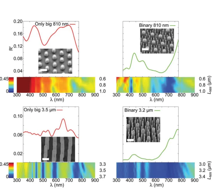
Fig. 4 Normal reflectance experimental curves for different VA-SiNWs heights of only big (left) and binary (right) arrays, with the same interspacing as in Fig. 3a. Each curve is compared with simulations, below the experimental curves, accounting for a tolerance on the height of the VA-NW, LNW,
of ±0.2μm. The insets show SEM pictures (1 μm-scale bars) of the substrates.
only big microgels (Fig. 4). The experimental spectra are the average of three measurements taken over different parts of the same substrate. Details of the simulations and experi-mental procedures are in the ESI, and Fig. S12,† together with the full simulated spectra for a broad range of NW heights
from 400 nm to 12 μm. The simulated spectra for the arrays
with big particles only show that there are transverse
reso-nances of the NWs in the visible range (i.e.λ from 390 nm to
750 nm), that weakly depend on the NW height. The experi-mental spectra reproduce the qualitative features of the simu-lated spectra, but with a broadening of the spectral peaks, due to polydispersity in the NW geometrical parameters and inter-spacing compared to the simulation (details of this effect are given in Fig. S13 in the ESI†). The most striking feature of the spectra for the binary NW arrays is that the overall reflectance is greatly reduced by the presence of the smaller NWs, indicat-ing the possible use of the binary arrays for anti-reflective coat-ings. This effect is particularly pronounced for the longer NWs, while the shorter NWs are specifically reducing reflec-tance around 400 and 700 nm. The dark-field reflecreflec-tance is also reduced by the presence of the smaller NWs, that partly disrupt the grating effect caused by the bigger NWs (see Fig. S13†). By varying the dimensions of the wires one can expect to tune the anti-reflective properties of the patterned surfaces.
To demonstrate further the potential of our sequential fab-rication method as a versatile nanopatterning tool, we used the gold core–shell nanoparticles instead of the small
micro-gels to form the binary lattices (Fig. 5a). Upon removing all the
organic material via 30 min of O2plasma (Fig. 5b), the binary
microgel arrays are transformed into honeycomb lattices of the gold cores. By tuning the compression of the gold core–shell microgels, we produced patterns with increasing density of metallic nanoparticles. These patterns might be interesting for a variety of applications, including the realization of plasmo-nic surfaces with fine and continuous tuning of the lattices.
To conclude, this work shows that it is possible to pre-program sequential assemblies of various types of microgels at fluid interfaces, transfer them onto silicon substrates and thus realize complex non-close-packed binary nanopatterns. We showed that the transferred structures can be used as lithogra-phical etching masks, enabling the controlled growth of binary nanowire arrays, with combinatorial control on their geometrical parameters, including their height, using MACE. The same assembly and patterning strategy can be applied to the realization of additional nanostructures. We expect that the extension of sequential particle assembly and deposition routes harnessing fluid interfaces will open up many interdis-ciplinary opportunities for the realization of complex nanopat-terns for applications in optics, material science, sensing and nano-bio cellular interfaces.
Con
flicts of interest
There are no conflicts to declare.
Fig. 5 (a) 20 × 20μm2AFM height images from a decoupled continuous gradient, where the big microgels were kept at a constant surface pressure
value of 1 mN m−1, while gold-core small microgels were compressed from 2 to 21 mN m−1from left to right. (b) Honeycomb gold nanoparticle pat-terns on the silicon substrate obtained after 30 min of O2plasma etching of the substrate in (a).
Acknowledgements
Authors thank N. D. Spencer, A. Studart and M. Fiebig for access to instrumentation. L. I., R. E. and M. A. F. R acknowl-edge the financial support of the Swiss National Science Foundation Grants PP00P2_144646/1, PP00P2 172913/1 and IZK0Z2_171156 and of the Swiss Government Excellence Postdoc Scholarship 2016.0246. K. G. and W. R. thank the German Research Foundation (Collaborative Research Center SFB985). R. E acknowledge the Australian Research Council for his DECRA (DE170100021). This work was performed in part at the Melbourne Centre for Nanofabrication (MCN) in the Victorian Node of the Australian National Fabrication Facility (ANFF).
References
1 A. D. Law, D. M. A. Buzza and T. S. Horozov, Phys. Rev. Lett.,
2011,106, 128302.
2 J. Fornleitner, F. Lo Verso, G. Kahl and C. N. Likos, Soft
Matter, 2008,4, 480–484.
3 L. Assoud, F. Ebert, P. Keim, R. Messina, G. Maret and
H. Löwen, J. Phys.: Condens. Matter, 2009,21, 464114.
4 F. Ebert, G. Maret and P. Keim, Eur. Phys. J. E: Soft Matter
Biol. Phys., 2009,29, 311–318.
5 S. Mazoyer, F. Ebert, G. Maret and P. Keim, Eur. Phys. J. E,
2011,34, 101.
6 L. J. Bonales, F. Martínez-Pedrero, M. A. Rubio, R. G. Rubio
and F. Ortega, Langmuir, 2012,28, 16555–16566.
7 N. Vogel, M. Retsch, C.-A. Fustin, A. del Campo and
U. Jonas, Chem. Rev., 2015,115, 6265–6311.
8 D. Wang and H. Möhwald, Adv. Mater., 2004, 16, 244–
247.
9 G. Zhang, D. Wang, Z.-Z. Gu and H. Möhwald, Langmuir,
2005,21, 9143–9148.
10 T. Honold, K. Volk, M. Retsch and M. Karg, Colloids Surf.,
A, 2016,510, 198–204.
11 J. J. Urban, D. V. Talapin, E. V. Shevchenko, C. R. Kagan
and C. B. Murray, Nat. Mater., 2007,6, 115.
12 M. Xie, X. Xiong, L. Yang, X. Shi, A. M. Asiri and X. Sun,
Chem. Commun., 2018,54, 2300–2303.
13 N. Fukata, T. Subramani, W. Jevasuwan, M. Dutta and
Y. Bando, Small, 2017,13, 1701713.
14 R. Elnathan, B. Delalat, D. Brodoceanu, H. Alhmoud, F. J. Harding, K. Buehler, A. Nelson, L. Isa, T. Kraus and
N. H. Voelcker, Adv. Funct. Mater., 2015,25, 7215–7225.
15 R. Elnathan, L. Isa, D. Brodoceanu, B. Delalat, F. Harding, T. Kraus and N. Voelcker, ACS Appl. Mater. Interfaces, 2015, 7, 23717–23724.
16 J.-H. Lee, A. Zhang, S. You and C. Lieber, Nano Lett., 2016, 16, 1509–1513.
17 Z. Dai, Y. Li, G. Duan, L. Jia and W. Cai, ACS Nano, 2012,6,
6706–6716.
18 J. Yu, Q. Yan and D. Shen, ACS Appl. Mater. Interfaces, 2010, 2, 1922–1926.
19 M. Kim, S. Im and O. Park, Adv. Mater., 2005,17, 2501–
2505.
20 V. Lotito and T. Zambelli, Langmuir, 2016,32, 9582–9590.
21 K. Volk, J. P. Fitzgerald, M. Retsch and M. Karg, Adv.
Mater., 2015,27, 7332–7337.
22 L. Isa, K. Kumar, M. Müller, J. Grolig, M. Textor and
E. Reimhult, ACS Nano, 2010,4, 5665–5670.
23 C. Haginoya, M. Ishibashi and K. Koike, Appl. Phys. Lett.,
1997,71, 2934–2936.
24 M. Ray and L. Jia, Adv. Mater., 2007,19, 2020–2022.
25 X. Li, T. Wang, J. Zhang, X. Yan, X. Zhang, D. Zhu, W. Li,
X. Zhang and B. Yang, Langmuir, 2010,26, 2930–2936.
26 J.-T. Zhang, L. Wang, J. Luo, A. Tikhonov, N. Kornienko
and S. A. Asher, J. Am. Chem. Soc., 2011,133, 9152–9155.
27 L. Scheidegger, M. A. Fernandez-Rodriguez, K. Geisel, M. Zanini, R. Elnathan, W. Richtering and L. Isa, Phys.
Chem. Chem. Phys., 2017,19, 8671–8680.
28 K. Geisel, L. Isa and W. Richtering, Langmuir, 2012, 28,
15770–15776.
29 M. Rey, M. A. Fernandez-Rodriguez, M. Steinacher, L. Scheidegger, K. Geisel, W. Richtering, T. M. Squires and
L. Isa, Soft Matter, 2016,12, 3545–3557.
30 M. Rey, R. Elnathan, R. Ditcovski, K. Geisel, M. Zanini, M. A. Fernandez-Rodriguez, V. V. Naik, A. Frutiger, W. Richtering, T. Ellenbogen, N. H. Voelcker and L. Isa,
Nano Lett., 2016,16, 157–163.
31 Z. Huang, N. Geyer, P. Werner, J. de Boor and U. Gösele,
Adv. Mater., 2010,23, 285–308.