HAL Id: hal-02384186
https://hal.archives-ouvertes.fr/hal-02384186
Submitted on 28 Nov 2019HAL is a multi-disciplinary open access archive for the deposit and dissemination of sci-entific research documents, whether they are pub-lished or not. The documents may come from teaching and research institutions in France or
L’archive ouverte pluridisciplinaire HAL, est destinée au dépôt et à la diffusion de documents scientifiques de niveau recherche, publiés ou non, émanant des établissements d’enseignement et de recherche français ou étrangers, des laboratoires
graphene oxide
Shashank Shekhar, Hyungwoo Lee, Duckhyung Cho, Myungjae Yang, Minju
Lee, Seunghun Hong
To cite this version:
Shashank Shekhar, Hyungwoo Lee, Duckhyung Cho, Myungjae Yang, Minju Lee, et al.. Nanoscale mapping of noise-source-controlled hopping and tunneling conduction in domains of reduced graphene oxide. Carbon, Elsevier, 2019, 148, pp.326-335. �10.1016/j.carbon.2019.03.087�. �hal-02384186�
Nanoscale mapping of noise-source-controlled hopping and tunneling conduction in domains of reduced graphene oxide
Shashank Shekhar, Hyungwoo Lee, Duckhyung Cho, Myungjae Yang, Minju Lee, Seunghun Hong
PII: S0008-6223(19)30311-2
DOI: https://doi.org/10.1016/j.carbon.2019.03.087
Reference: CARBON 14078 To appear in: Carbon
Received Date: 26 October 2018 Revised Date: 7 March 2019 Accepted Date: 27 March 2019
Please cite this article as: S. Shekhar, H. Lee, D. Cho, M. Yang, M. Lee, S. Hong, Nanoscale mapping of noise-source-controlled hopping and tunneling conduction in domains of reduced graphene oxide,
Carbon (2019), doi: https://doi.org/10.1016/j.carbon.2019.03.087.
This is a PDF file of an unedited manuscript that has been accepted for publication. As a service to our customers we are providing this early version of the manuscript. The manuscript will undergo copyediting, typesetting, and review of the resulting proof before it is published in its final form. Please note that during the production process errors may be discovered which could affect the content, and all legal disclaimers that apply to the journal pertain.
M
AN
US
CR
IP
T
AC
CE
M
AN
US
CR
IP
T
AC
CE
PT
ED
Nanoscale mapping of noise-source-controlled hopping and
tunneling conduction in domains of reduced graphene oxide
Shashank Shekhar†
, Hyungwoo Lee†
, Duckhyung Cho, Myungjae Yang, Minju Lee and Seunghun
Hong*
Department of Physics and Astronomy, and Institute of Applied Physics, Seoul National University, Seoul 08826, Korea
*Corresponding author. Tel: +82 874-5562 E-mail: seunghun@snu.ac.kr
†
M
AN
US
CR
IP
T
AC
CE
PT
ED
ABSTRACTWe report a nanoscale mapping of noise-source-controlled transport characteristics in the domains of reduced graphene oxide by utilizing noise-source imaging strategies. In this method, current and noise images were measured simultaneously using a scanning noise microscopy and analyzed to map sheet−resistances (R ) and noise−source densities (neff). The maps showed the
formation of conducting and insulating domains, where the insulating domains exhibited up to three-four orders of higher R and neff than those of conducting domains. Interestingly, the
sheet−conductance (Σ ) and neff followed rather opposite power−law behaviors like Σ ∝ neff−0.5
and Σ ∝ neff0.5in conducting and insulating domains, respectively, which could be attributed to
the difference in mesoscopic charge transport mechanisms controlled by neff in domains. Notably,
high biases resulted in the increased conductance (∆Σ ) and decreased noise−source density (∆neff) following a relationship like ∆Σ ∝−∆neff0.5 for both conducting and insulting domains,
which could be explained by the passivation of noise−sources at high biases. Furthermore, ∆Σ
versus ∆neff plot on the annealing also followed a power−law dependence (∆Σ ∝−∆neff0.5) in
conducting domains, which could be attributed to carrier generation on the annealing. Our results about mesoscopic charge transports could be significant advancements in fundamental researches and applications.
Keywords: reduced graphene oxide, electrical noise, charge transport, scanning noise
M
AN
US
CR
IP
T
AC
CE
PT
ED
1. IntroductionReduced graphene oxide (RGO) is one of the most promising materials in nanoelectronics, and has been widely studied in materials science, electronics, chemistries, and biologies [1−16]. Previous studies showed that RGO has versatile exotic chemical and physical properties such as a high charge storage capacity, a tunability in electrical properties, a high chemical reactivity, an optical transparency and a mechanical flexibility [1−16]. In addition, the large scale fabrication of RGO devices is possible in a short span of time under ambient conditions via solution processing methods [6−12]. Owing to various remarkable properties, RGO has been used in versatile applications such as high−performance supercapacitors, memory devices, highly−sensitive biological and chemical sensors, and high-performance solar cells [1,4−8]. RGO films have rich microstructures due to the presence of the various kinds of functionalities and the ordered sp2 and disordered sp3 hybridization of carbon bondings [4−8]. Recent works have shown significant local variations in currents in a RGO thin film [9]. Therefore, the nanoscale investigation of the transport properties of RGO should be essential for the further understanding and improvement of RGO−based devices. However, still a little is known about the transport properties of RGO at a nanoscale domain−structure level.
On the other hand, electrical noises, the temporal fluctuations, in the currents provide useful information about materials and devices, and those noises are helpful in understanding charge traps or noise−source densities, charge inhomogeneities, carrier types and densities in devices [17−20]. In a RGO film, various localized noise−sources such as structural defects, electronic traps, functionalities, and impurities are distributed in different domains, generating electrical
M
AN
US
CR
IP
T
AC
CE
PT
ED
noises [20−27]. Previously, there have been some studies about the noises in RGO devices, and it has been observed that the noise behaviors depend on the presence of functional groups and disorders in the RGO [15−17]. However, it has been very difficult to identify and map the activities of such localized noise−sources in a RGO film at a nanoscale resolution. Recently, we have developed a scanning noise imaging method [18−20,27], allowing us to map the localized noise−sources in domains and boundaries of graphene [20] and polymers [19]. Noise−source mappings further helped us in understanding transport mechanisms in conducting channels. However, the nanoscale effects of noise−sources on mesoscopic transport behaviors in the various domains of RGO have not been explored yet.
Herein, we report a nanoscale direct mapping of the noise−source controlled charge transports in domains of the RGO film, showing hopping and tunneling conduction mechanisms in
conducting and insulating domains, respectively. In our strategy, firstly, the images of electrical
currents and noises on RGO films were measured simultaneously using a scanning noise microscopy (SNM) [18−20] and analyzed to map the sheet−resistance (R ) and noise−source density (neff). The measured maps showed the conducting and the insulating domains, where the
insulating domains exhibited up to three orders of magnitude higher R and neff than those of the
conducting domains. Notably, we observed opposite power law relationships like Σ ∝ neff−0.5
and Σ ∝ neff0.5 in conducting and insulating domains, respectively. The results were attributed to
the variations in mesoscopic charge transports controlled by the neff in the RGO domains.
Interestingly, the increased bias voltage resulted in the increased conductivity ∆Σ and decreased noise−source density ∆neff with a relationship like ∆Σ ∝−∆neff0.5 in both conducting and
insulating domains, which was explained by the passivation of noise−sources at the high bias voltage. The thermal annealing process increased the area of conducting domains. Most of the
M
AN
US
CR
IP
T
AC
CE
PT
ED
annealed regions exhibited increased conductivity and decreased noise−source density, while the conducting domains exhibited the relationship like ∆Σ ∝−∆neff0.5. These results show that
charge transports and noise−sources are closely related, and the noise−source activities even play a determinant role in the nanoscale charge transport phenomena of RGO films. These results provide valuable insights about the effect of noise−sources on mesoscopic transports and should have significant impacts on fundamental researches and applications.
2. Methods
2.1 Device fabrication
We purchased graphene oxide (GO) dispersed in water from Graphene Supermarket (Calverton, NY, USA) for fabricating devices. The concentration of purchased GO solution was 6 mg/ml. The solution was diluted in DI water to 2 mg/ml via sonication for 10 minutes. Then, GO solution of concentration 2 mg/ml in DI water was dropped on a clean Si/SiO2 substrate (oxide
thickness ~100 nm). The dropped solution on the substrate was kept idle for 30 seconds. Then, the GO was spun coated on the substrate with 2000 rpm for 60 seconds. To obtain RGO, the spin coated GO was reduced by an annealing inside the quartz furnace tube at 450 °C for 60 minutes under the flow of argon (Ar) gas (10 ml/s). The furnace tube was rapidly heated up to a target temperature of 450°C at the rate of 32.5 °C/min under a constant Ar flow (10 ml/s). A metal electrode (50 nm Au on 3 nm thick Ti) was deposited by thermal evaporation through a shadow mask. It is to be mentioned here, that we did not use any lithographic process to keep the RGO surface clean for electrical measurements.
M
AN
US
CR
IP
T
AC
CE
PT
ED
Fig. 1. Schematic diagram showing the experimental set−up for the nanoscale mapping of noise−source activities and sheet resistances in the conducting and insulating domains of RGO device channels. A small DC bias was applied between the Au electrode and Pt tip. AC signals were observed in the output due to the noises and recorded by a home built network analyzer capable of measuring noises in real time as a function of probe positions.
Fig. 1 shows a schematic diagram of a set−up for the current and the noise imaging on a RGO device. For measurements, a platinum (Pt) tip installed on a conducting AFM (XE−70, Park Systems) was made a direct contact on the surface of the RGO device. To achieve a stable electrical contact, a Pt tip was used (25Pt300B, Park Systems) as a probe instead of commonly used metal coated tips of which metal coating can be peeled out easily during the scanning. After the probe made a contact on the RGO surface, a bias voltage (0.4 V) was applied to the metal electrode of the sample by a function generator (DS345, Stanford Research Systems). During all imaging and measurements in this article, the contact force was maintained at 1 µN via an AFM force feedback circuit. Typically, the tip scanned in the area of 3 µm × 3 µm with the scan rate of 0.2 Hz. The electrical currents through the Pt probe were measured and converted to amplified voltage signals by using a low−noise pre−amplifier (SR570, Stanford Research Systems). The
M
AN
US
CR
IP
T
AC
CE
PT
ED
topography and the noise images were simultaneously recorded. The electrical noises, fluctuating components of the current signals, were collecting using a band-pass filter (6dB) in the SR570 preamplifier, and the RMS power of the collected signals was obtained by a homemade RMS-to-dc converter built using an AD737 chip (purchased from Analog Devices). Note that the obtained noise power was the integrated value of noise (power spectral density) PSDs over the frequency (f) range of the pass band of the band−pass filter. By dividing the square of the measured RMS noise power with the bandwidth of the band pass filter, we obtained the noise PSD at the central frequency of the band. Finally, the measured current and noise PSD maps were analyzed using a network model to obtain the R and neff maps of the domains of RGO.
3. Results and discussion
3.1 Nanoscale mapping of sheet−resistances and noise−source activities in domains of RGO
Fig. 2a shows an atomic force microscopy (AFM) topography image of a thin layer of the RGO film. The image shows a clean surface with its roughness of ~1 nm which is a typical value for an individual RGO layer [28]. The scanning electron micrograph (supplementary information Fig. S1) also shows clean surfaces without any cracks or residues, indicating the high quality of our RGO samples.
Fig. 2b shows the corresponding current map of the RGO film. For the current mapping, the bias voltage of 0.4 V was applied to the metal electrode and the current output was measured using the conducting (Pt) AFM tip. The current map showed two distinctive regions with low (of the order of nA) and high currents (of the order of µA) separated by boundaries. The high current carrying areas (bright yellow regions) with average width ~500 nm could be the ordered
M
AN
US
CR
IP
T
AC
CE
PT
ED
conducting domains of the RGO, whereas low currents areas (dark regions) could belong to disordered insulating domains. The origin of high current regions could be the formation of sp2 rich carbon atoms in the RGO, as predicted previously [7,12]. The sp2 hybridization of the orbitals is responsible for high conductions in carbon allotropes. Previous works using c−AFM, Raman spectroscopy, near field scanning optical microscopy and electron microscopies show that RGO consists of conducting (sp2−rich) and insulating (sp3−rich) domains of similar sizes [7,9,14,29-31]. Also, a similar structure model is proposed in RGO based on conducting and insulating domains [7]. Our results clearly show the formation of conducting and insulating domains in the RGO demarcated by the boundaries.
M
AN
US
CR
IP
T
AC
CE
PT
ED
Fig. 2. Nanoscale mapping of sheet−resistances (R ) and noise−source activities in RGO.(a) Contact mode AFM image of a RGO surface. The surface roughness was of the order of 1 nm due to wrinkles. (b) Current image of the RGO surface at the applied bias of 0.4 V. Different current levels were measured on the RGO surface showing the formation of conducting and insulating domains. (c) I−V curves of the
conducting and insulating domains. The I−V curve of the conducting domain was linear as the slope of the
curve on a log-log scale was ~1. The I−V curve of the insulating domain showed a linear behavior only at
low voltages (< 0.4 V), and I increased as ∼V4 at higher voltages. (d-i) R map of the RGO surface. The
R map showed high values in the insulating domains and boundaries. (d-ii) High resolution R map. The
high resolution R map showed that the conducting domain had R ∼104−105Ω/ . The insulating domains
showed nearly 3−4 orders higher R than that of the conducting domain. (e) Current−normalized noise
PSD map measured at ∼17.2 Hz. The insulating domains showed high values (∼10−2 Hz−1) of PSD. (f-i)
Noise−source density (neff) map. The map was calculated from the measured current−normalized noise
PSD and sheet−resistance maps. The insulating domains showed the high neff as compared to the
conducting domains (f-ii) High−resolution neff map. The neff in insulating domains were 2−3 orders higher
than that in the conducting domains. The insulating domains have oxygen functional groups, structural
defects and disorders, which could lead to high noise−sources. (g) Σ versus neff plots for conducting and
insulating domains showing power law dependences (Σ ∝ nefft), separately. The black and red circles
represent data points from conducting and insulating domains, respectively. The exponent t is −0.5 and 0.5 for conducting and insulating domains, respectively. The different exponents were attributed to
the difference in the conduction mechanism due to neff. Scale bars are 1µm.
Fig. 2c is a typical current−voltage (I−V) curve of conducting and insulating domains. To
perform this measurement, voltage on the electrode was swept while keeping the Pt tip stationary on a conducting or an insulating domain. The positions of the tip in conducting and insulating
M
AN
US
CR
IP
T
AC
CE
PT
ED
domains were marked by dotted black and white circles in the Fig. 2b, respectively. The I−V
curve of a conducting domain was linear in the voltage range of 0−4.5 V. However, the insulating domain showed two different kinds of dependence in the measured voltage range. At low voltages (below 0.4 V), the I−V curve was linear as it was evident from the slope of ∼1 in logI versus logV plot. The current increased rapidly above 0.4 V and became non−linear. At high voltages, I increased as V4 (slope of logI versus logV is ∼4, i.e. I ∝ V4). It is to be noted that at high voltages, the current of insulating domains rapidly approached to the value of that of the conducting domains. These results implicate that the non−linear I−V characteristics of the RGO
device arose due to the presence of insulating domains. The sudden rise in the current at higher voltages could be attributed to excess injected carriers in the insulating domains as reported previously [26].
In our previous work, we developed a computational iterative method to calculate a sheet resistance R map from a current map on a two−dimensional conducting channel [20]. Taking advantage of the method, we could obtain R maps from the current maps, showing the spatial distribution of R in RGO. The details of the calculation method are described in the supplementary information and supplementary Fig.S2, S3 and S4.
Fig. 2d (i) and (ii) shows R maps on the RGO film, obtained from the current maps Fig. 2b and supplementary Fig.S5, respectively. In the maps, the conducting and insulating domains could be clearly distinguished. The averaged sheet resistance value in the conducting domains was ∼107 Ω/ , which is consistent with the previously−reported sheet resistance of RGO on a SiO2 substrate [7,8]. On the other hand, the sheet resistance value in the insulating domains was
estimated as ∼108 Ω/ and it was about an order of magnitude higher than that inside the conducting domains. This implies that insulating domains in a RGO film can obstruct the
M
AN
US
CR
IP
T
AC
CE
PT
ED
conduction of charge carriers, increasing the total electrical resistance of the RGO film. Presumably, the oxygen functional groups and other structural disorders in an insulating domain can act as carrier scattering centers obstructing charge conductions, resulting in the high R in a domain.
Fig.2e shows a map of SI/I2 (at ∼17.2 Hz) obtained from the noise PSD map measured
simultaneously with the current map. Fig. 2b. Here, we first measured the map of noise PSD (SI)
at ∼17.2 Hz via the noise microscopy, and divided the measured SI map by the square of the
current map to obtain the SI/I2 map. During the measurement, the bias voltage of a 0.4 V was
applied to the electrodes. In the conducting domains, the SI/I2 values were ∼10−6 Hz−1 which is
comparable to the previously-reported SI/I2values on a pristine graphene [20,23−25]. On the
other hand, the insulating domains in the RGO exhibited the SI/I2 values of ∼10−2 Hz−1 which is
much higher than the SI/I2 in the conducting domains. This implies the higher activities of
electrical noise−sources in insulating domains than in the conducting domains of RGO. Any electrical potential barriers or structural defects, which can produce charge scattering with a relatively long trapping time, can produce fluctuation in electrical currents, thus generating electrical noises. For example, it is reported that the electrical and structural inhomogeneities and defects produce localized electronic states which can trap charge carriers for certain time periods [17,25]. Such localized states produced by electrical and structural defects or scattering are collectively termed as noise-sources. Previous works suggested that an insulating domain in RGO has abundance of lattice disorders, dangling bonds, and chemical functional groups [7−12]. Such nanostructured defects in the insulating domain can provide localized electronic states and act as charge traps which randomly trap and release charge carriers in the domain [10,16]. The activities of such charge traps can generate electrical−noises by generating random fluctuations
M
AN
US
CR
IP
T
AC
CE
PT
ED
in the charge carrier number in the domain, and thus they can be the origin of the high SI/I2
values in the insulating domains.
Further using the SI/I2 maps, we calculated effective charge trap density (neff) maps showing
the quantitative distribution of electronic traps generating electrical noises in the domains of the RGO film. Fig. 2f (i) and (ii) show neff maps on the RGO film, obtained from the SI/I2 maps in Fig. 2e and supplementary Fig.S6, respectively. The detailed calculation method for the neff is
shown in the supplementary information. In brief, we modeled the RGO film as a two−dimensional network on a x−y plane comprised of small RGO segments of a square shape
with its area of (∆l)2. A RGO segment at a (x, y) was assumed to have a sheet resistance R (x, y) and an effective noise−source density neff(x, y). Each node at a (x, y) can be considered as a point
where a conducting AFM tip was placed to measure I(x, y) and SI (f, x, y) in our experiments.
Each node at (x, y) was connected with four neighboring nodes through small RGO channels with its area of (∆l)2, a sheet resistance R (x±∆l/2, y±∆l/2), and effective noise−source density
neff(x±∆l/2, y±∆l/2). We can estimate that each connecting RGO channel has a resistance of ∆R
∼R , and it generates the current noise of ∆ =
∆ ∙ ∆ with the total carrier
number ∆C in the small segment of area ∆ . Furthermore, assuming that ∆l is small, the sheet
resistance and the effective noise−source density of each RGO segment at (x, y) can be approximated as the averaged values of those of four RGO channels at (x±∆l/2, y±∆l/2)
connecting the node with four neighboring nodes. Using the estimated R (x, y) values (Fig. 2d (i) and (ii)), the effective noise−source density neff(x, y) at each point could be calculated from the SI(f, x, y) values at the corresponding node at (x, y) (details in the supplementary information).
M
AN
US
CR
IP
T
AC
CE
PT
ED
conducting domains exhibited neff values in the range of ∼1011 to 1013 cm−2eV−1. On the other
hand, the insulating domains exhibited rather high neff values in the range of ∼1013 to 1015
cm−2eV−1. At the domain boundaries, the neff was about ∼1015 cm−2eV−1. In a quantitative
manner, the results directly show that the density of electronic traps is much higher in the insulating domain in RGO than in the conducting domain, which has been only theoretically estimated before. The lattice disorders, dangling bonds, and chemical functional groups, which are abundant in the insulating domains, could act as electronic traps and result in the high neff in
the domains, as suggested in previous works [10−16].
Fig. 2g is a scatter plot showing the relation between the effective noise−source density neff
and the sheet−conductance Σ on a RGO film. Each data point in the plot shows a pair of neff and
Σ values at an individual position on the RGO film. The data from the conducting and
insulating domains were plotted with black and red colors, respectively. The solid lines are the
least square fittings. To obtain the digital data in a domain, we selected and cropped the maps of that particular domain from both Σ and neff maps. The digital data of the maps of a domain were
utilized for plotting purposes. In the conducting domains, an inverse correlation between the neff
and Σ was observed. Here, nearly two orders of magnitude variation in Σ was observed, which could be associated with nearly four orders of magnitude variation in the neff. By fitting the data,
we found that Σ was approximately proportional to the neff−0.5 as indicated with a yellow line in
the Fig. 2g. On the other hand, in the insulating domains, a direct correlation between the neff and
Σ was observed, which is in opposite to the result in the conducting domains. The Σ was approximately proportional to the neff0.5 in the insulating domains as indicated with a black line
M
AN
US
CR
IP
T
AC
CE
PT
ED
can be a key factor determining the electrical conductivity in the domains of the RGO, and noise−sources could have a completely contrasting role in conducting and insulating domains.
In RGO, the dominant charge transport mechanism can be hopping [12]. In a conducting domain of RGO, a large number of hopping states exist. Thus, the charge carriers mainly flow through the hopping states and the trap-to-trap transition of carriers is limited [32−36]. In this case, the charge traps obstruct the charge conduction by reducing the carrier mobility [34,36]. Further, previous works based on an effective medium approximation theory [36] show that the mobility (µ) can be inversely proportional to the square root of the charge trap density as
µ ∝ neff−0.5, (1)
when the trap states have a Gaussian distribution in the energy domain with a rather large distribution width as reported for the RGO [37]. Note that the conductivityΣ is proportional to
neµ, and the conducting domains have nearly uniform carrier density (n) as carbon atoms have mostly sp2 bondings [9]. Thus, this result is consistent with our observation of Σ ∝ neff−0.5 in the
conducting domains. On the other hand, the insulating domains have only few numbers of hopping states and have a large number of trapping states. In this case, the charge conduction through the hopping states is limited, and charge carriers are mainly flown by tunneling from a trapping state to another trapping state [37−40]. In such trap−to−trap conduction, the carrier mobility can have a direct correlation with the trap density as traps assist in conduction [38−41]. Particularly, when the trap density is rather high as in the insulating domains of RGO, the mobility µ can be proportional to the square root of the charge trap density [36]. Then, the relationship Σ ∝ neff0.5 is consistent with our result. It is also worth mentioning that our results
are consistent with previous studies about the electrical characteristics of RGO with varying temperature measurements [42,43].For example, previous works show that the electrical
M
AN
US
CR
IP
T
AC
CE
PT
ED
transport of the RGO at different temperatures strongly depends on trap or noise-source densities which are determined by the reduction status of RGO. At a low reduction status when noise-source density is high, an activated conduction is observed in the RGO at a room temperature, which was attributed to the trap-to-trap transition of carriers. At a low temperature or in a highly-reduced GO film, there are not sufficient energy states for a direct transition among the traps, and hopping mechanism dominates. In this case, conducting domains and hopping of carriers can determine the conduction mechanism. On the other hand, at a room temperature, the insulating domains and trap-to-trap transition could contribute dominantly to the electrical conduction, which is consistent with our works [42,43]. These results provide important insights about the role of electronic traps as dominant noise−sources on the charge transports in different domains of RGO. Considering that the noise−sources can be a critical factor determining the characteristics of RGO−based devices, our work should significantly contribute to the basic researches and applications of RGO.
M
AN
US
CR
IP
T
AC
CE
PT
ED
Fig. 3.Effect of bias voltages on the noise−source activities in the conducting and the insulating domains of RGO.(a) Sheet resistance map (R ) of the RGO at the bias voltage of 0.2 V. (b) R map of the RGO at the bias voltage of 2 V. The R decreased with increase in the bias voltage. At higher voltages, the R of insulating domains decreased and rapidly approached to that of the R of the conducting domains. (c) The noise−source density (neff) map at 0.2 V (d) The neff map at 2 V. The neff decreased up to three orders of
M
AN
US
CR
IP
T
AC
CE
PT
ED
and ∆neff plot. The∆Σ and ∆neff showed a power−law dependence following the relation ∆Σ ∝−∆neff 0.5
for
both conducting and insulating domains, which was attributed to the Fermi level shift due to noise−source
passivation. (f) Noise PSD versus frequency plot at different biases in conducting domains. At low
frequencies and low bias voltages the conducting domains showed a ∼1/f noise behavior, and PSD
decreased with increasing bias voltage. (g) Noise PSD versus frequency plot at different biases in insulating domains. The noise PSD decayed as 1/f in the insulating domain. At low voltages and low frequencies, a peak appeared in the noise−PSD versus frequency plots of the insulating domains. This peak could be attributed to additional relaxation processes originated from polar hydroxyl functional
groups (−OH, −COOH) attached to the insulating domains. Scale bars are 250 nm.
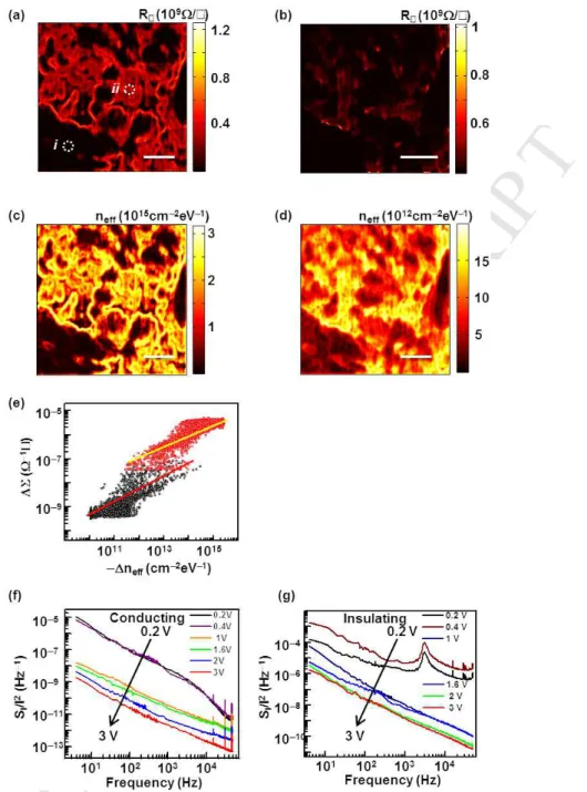
In order to estimate the effect of electric fields on the R , we mapped the R values at the bias voltages of 0.2 V and 2 V, as shown in the Fig.3a and 3b, respectively. The maps were calculated from corresponding current maps measured by the method described in supplementary information. The insulating domains showed R of the order of109Ω/ at the low bias (0.2 V). At the high bias of 2 V, we observed over two orders of magnitude decrease in the R (<107Ω/ ) in the insulating domains, as can be seen from the comparison of Fig. 3a and 3b. On the other hand, we did not observe any significant changes in R for conducting domains due to the increase in the voltage. Note that the R of the insulating domains drastically decreased and nearly approached to the values of those of the conducting domains at the high bias. The results show that the high bias affected the electronic transport of the RGO, mostly in insulating domains. The distinctive behavior of R in the insulating domain of RGO could be attributed to the presence of the high density of defects, functionalities and disorders creating a high potential barrier [13]. A high bias could have provided sufficient energies to charge carriers to overcome the barrier
M
AN
US
CR
IP
T
AC
CE
PT
ED
potential of insulating domains, resulting in enhanced carrier injections from the electrodes. Those injected carriers could outnumber intrinsic carriers in insulating domains resulting in rapid decrease in R [19,21,22].
To observe the effects of a high bias on a noise−source density, we mapped and compared the
neff values at the bias voltages of 0.2 V and 2 V, as shown in the Fig.3c and 3d, respectively. The
maps were calculated from the SI/I2 maps (supplementary Fig. S7) obtained from the same area
of the RGO device from which R map was measured in Fig. 3a. The maps show an overall decrease in neff of the RGO at a high bias. The insulating domains exhibited the high neff ∼1015cm−2eV−1at the low bias voltage of 0.2 V, whereas the neff decreased by nearly three orders
of magnitude at the high bias of 2 V. On the other hand, the neff values in the conducting domains
of the RGO decreased slightly at 2 V as compared to 0.2 V. The results indicate that the high bias voltage significantly affected the noise−source activities of the RGO. Presumably, noise−sources would have been passivated by excess injected carriers, leading to a large decrease in the neff at the high bias voltage [22,44−46]. Since insulating domains have rather many
noise−sources compared to conducting domains, we can expect the drastic decrease of the neff in
the insulating domains. It should be mentioned that such decrease in noise−sources at a high bias can make RGO devices advantageous for a high voltage operation because the most of organic materials−based devices exhibit increased noise−sources at a high bias.
Fig. 3e shows scatter plots of ∆Σ versus ∆neff in conducting (black curve) and insulating (red
curve) domains. Each data point in the plot represents a pair of ∆neff and ∆Σ values at the
individual positions of the RGO film. The Σ (or neff) map at 0.2 V was subtracted from
M
AN
US
CR
IP
T
AC
CE
PT
ED
power law (∆Σ ∝−∆nefft) between ∆Σ and ∆neff was observed in both conducting and insulating
domains. The least square fittings (solid lines) of the data indicate that exponent t of the fitting curves on a log−log scale were ∼0.5±0.1 for both conducting and insulating domains.
A high bias generates a large number of carriers in RGO, which could shift a Fermi level towards a conduction (valance) band when electrons (hole) are majority carriers [424−46]. Due to the shift in a Fermi level, traps and noise−sources whose energy levels are below the Fermi level would be passivated by charge carriers [44−46]. When a high bias is applied, there exist excess electrical carriers in a system. Hence, some fraction of the noise-sources can be effectively filled with the carriers and do not contribute to the noise generation. The passivation of noise-sources refers to such screening of the noise-sources by the excess carriers. Since a Fermi level in RGO is a slowly varying function of n [8], the Fermi level shift ∆EF is expected to
be small. Then, ∆neff and ∆n can be approximated as ∆neff=−A∆EF, ∆n = B∆EF and ∆n=−E∆neff
where A, B, and E are proportionality constants. A change in a conductivity by a bias voltage change can be written as
∆σ = eµhnh−eµlnl= e(µl+∆µ)(nl+∆n) − eµlnl= eµl∆n + enl∆µ +e∆µ∆n, (2)
where subscripts h and l stand for the high and low bias conditions, respectively. A low bias noise−source density neff_l can be expressed in terms of µl by equation (1) as, neff_l= .µl−2, where
D is a proportionality constant. A high bias can affect a noise−source density by a large extent, and it can also bring some change in a mobility [21,22,26]. Thus, a noise−source density at a high bias neff_h can be written as neff_h= .(µl +∆µ)−2. Assuming, ∆µ/µl<<1 and applying Taylor
M
AN
US
CR
IP
T
AC
CE
PT
ED
∆ = − = . . !" − . #$ ≈ − . &''_) = − .*&''_")/ (3)Thus, ∆µ dependence on neff can be approximated as ∆µ=−,. . $-/_#∆ . Substituting µ
and∆µ values in equation (2), we can obtain
∆σ= −.,/ _#
$ / ∆ − ,.
# $-/_#∆ + .,/ $-/ ∆ _#∆ . (4)
Analytically, a Fermi level shift can passivate more noise−sources if a noise−source density is high at that point. If the noise−source density change ∆neff is originating from the Fermi level
shift, then the ∆neff would be rather large at the places where the neff_l would be large.
Experimentally, we also observed the similar behavior showing a linear dependence between neff
and ∆neff (see supplementary Fig.S8). Thus, neff_l in equation (4) can be substituted by C∆neff,
where C is a proportionality constant. Then, equation (4) can be modified as
∆σ= −.,/1$ / ∆ / − ,.1$-/ #∆ $ / + .,/1$-/ ∆ / . (5)
If ∆neff is much larger than initial carrier density nl, which holds in our cases due to the
passivation of a large number of noise−sources at the high bias, we can neglect 2nd term in the equation (5) and it can be further simplified as
∆σ= −.,/1$ + .,/1$) ∆ / . (6)
This result indicates a relationship ∆σ ∝ ∆neff0.5, explaining our experimental results. Some
data deviate from the approximation, resulting in the broadening of data points in the plots. Interestingly, equation (6) is also valid for the plots of insulating domains, implicating that a similar hopping process could dominate transports in an insulating domain at a high bias. A high
M
AN
US
CR
IP
T
AC
CE
PT
ED
bias creates a plenty of carriers in insulating domains, and those carriers make hopping more favorable than trap-to-trap transitions [34].
Fig.3f and 3g show the frequency dependence of normalized noise PSD (SI/I2) at different
voltages in conducting and insulating domains, respectively. The spectra were measured using a fast-Fourier transform (FFT) spectrum analyzer (SR770, Stanford Research Systems), while keeping the stationary contact of the conducting AFM tip at the conducting (i) or insulating (ii) domains marked by dotted circles in the Fig. 3a. In the measured frequency range (1 Hz-10 kHz), the normalized PSD of a conducting domain as well as an insulating domain followed a f−β behavior for all voltage conditions (0.2 to 3V). The exponent β was estimated from the slopes of the spectra, ranging from 0.9 to 1.1. These results show that the conducting and the insulating domains of the RGO device had a typical 1/f noise behavior at low frequencies as previously reported, implying that the noises originated in the multiple noise−sources of varying relaxation times (trapping-de-trapping time) [15,16,20,24].
The noise PSD of both conducting and insulating domains were decreased by nearly four orders of magnitude as a bias voltage was increased from 0.2 to 3 V. Interestingly, a broad peak appeared at ∼3 kHz in the PSD spectra of the insulating domains at low voltages (0.2 to 0.4 V), whereas the peak did not exist in the spectra of the conducting domains. The voltage dependence of noise PSD reduction could be due to the passivation of noise−sources by a high bias [22]. The broad peak in the insulating domains could be attributed to the distribution of relaxation processes [47]. Usually, the relaxation function (ϕ) for a specific relaxation process decays exponentially and follows a relation like ϕ ∝ e−t/τwhere τ is the relaxation time [47,48]. The noise PSD of this relaxation process generates a Lorentzian noise of a type 2τ/[1+(2πfτ)2], and numerous such relaxation processes having different τ result in the 1/f kind of noise [40]. On the
M
AN
US
CR
IP
T
AC
CE
PT
ED
other hand, previous works show that heterogeneities, organic functionalities and disorders in the RGO could produce a different kind of relaxation process which decays non−exponentially (e.g. polynomial etc) [47,48]. In an insulating domain of the RGO, the different clusters of atoms with –OH and −COOH groups (2−4 nm of size) could cooperatively produce additional non−exponential relaxations [49−51]. Such relaxation process generates a broadened peak in a noise PSD versus frequency spectrum [47,49,51].
M
AN
US
CR
IP
T
AC
CE
PT
ED
Fig. 4. Effect of thermal annealing on the sheet resistance and noise−source activities in the conducting and the insulating domains of RGO channels. Column 1 shows the images from RGO annealed for 15 minutes, whereas 2nd column shows images from subsequent 30 minutes annealed sample (a,b) Sheet-resistance (R ) maps of RGO device annealed for 15 minutes and subsequently annealed for 30 minutes at
450 oC, respectively at the same region. We can clearly see the growth and expansion of the conducting
domains on the annealing (for an eye guideline one such conducting domain is marked with dotted line in Fig.4a and 4b). At a short annealing time the sizes of the conducting domains were < 100 nm. The longer
annealing time significantly decreased R . (c) Noise−source density (neff) map of the RGO device
M
AN
US
CR
IP
T
AC
CE
PT
ED
of the RGO device annealed for subsequent 30 minutes. The neff reduced significantly on further
annealing for 30 minutes. As the conducting domains evolved on heating, lower neff values were observed
in those regions. (e) The ∆Σ versus ∆neff plot on the annealing. ∆Σ versus ∆neff showed two different
kinds of dependence in conducting and insulating domains. The conducting domain showed a scaling behavior ∆Σ∝−∆neff
0.5
due to an increase in the carrier number and shift in the Fermi level on an annealing. The dependence was uncorrelated in the insulating domains. Scale bars are 250 nm.
Fig. 4a shows the R map of the RGO sample annealed for 15 minutes. Fig. 4b is the R map of the same region after subsequent annealing for 30 minutes. The furnace tube was rapidly heated up to the target temperature of 450 °C at a rate of 32.5 °C/min, and the RGO was annealed at the temperature for different time periods under the flow of argon (Ar) gas (10 ml/s). We made scratch marks on the device to identify a specific location and used them to come back to the same area for mapping after the annealing process. A bias voltage of 0.4 V was applied during electrical measurements. Most of the part of the RGO (Fig. 4a) showed R values higher than 109Ω/ in the sample annealed for 15 minutes. Only a few tiny patches of conducting domains of average size ∼100 nm exhibited R values below 108Ω/ . Since the boundaries of the conducting domains had large R (~108Ω/ ), the conducting domain could be easily visualized in the Fig. 4a and 4b. One of the conducting domains is marked by blue dotted lines in Fig. 4a and 4b. When the RGO sample was subsequently annealed for another 30 minutes (Fig.4b), the conducting domains became larger and exhibited rather low R (∼106Ω/ ) values. The insulating domains also showed a considerable decrease in R and most of the regions of the insulating domains exhibited R values below 108Ω/ after annealing for 30 minutes. The results show that the annealing of the RGO could restore the conductivity in both conducting and insulating
M
AN
US
CR
IP
T
AC
CE
PT
ED
domains of the film. It has been previously reported that during the annealing process, the oxidized regions of the GO can be slowly converted to the sp2 configuration which leads to the delocalization of the carriers [7−9]. Further, the conducting domains grow in the size and contributed in the electrical conduction [7−9]. Previously, it was reported that the annealing of the RGO produces large conducting domains which are rich in sp2 hybridized carbon atoms [9,29-31]. Hence, annealing process increases the concentration of delocalized π electrons due to the formation of large sp2 conducting domains. In a way, an annealing process is similar to a doping process and increases the carrier concentration, resulting in a small shift in the Fermi level. Note that the R maps in our method allowed us to monitor the microscopic changes in the domains of the RGO on an annealing, providing important insights about the growth mechanism and electrical conduction of the domains.
Fig. 4c shows the neff map of the RGO annealed for 15 minutes. The neff map was calculated
from SI/I2 map (supplementary Fig. S9) obtained on the same area where the R map in the
Fig.4a was measured. Most of the regions on the RGO film exhibited a rather large noise−source density neff of ∼1015 cm−2eV−1. However, small conducting domains with relatively low neff were
also found surrounded by boundaries with high neff of ∼3×1015 cm−2eV−1. The high neff implicates
insufficient reduction of GO films annealed for 15 minutes. The functional groups and lattice disorders are the main sources of noises in the RGO, and insufficient annealing time may result in a rather high density of such noise−sources. Our results indicate that the annealing of GO initiates the formation of conducting domains as well as the reduction of noise−sources.
Fig. 4d shows the neff map of the RGO after a subsequent annealing for 30 minutes at 450 oC.
M
AN
US
CR
IP
T
AC
CE
PT
ED
lower than 1014 cm−2eV−1, indicating that overall neff decreased by nearly two orders. The
conducting areas with a low neff became larger and their boundaries got extended. The central
regions of conducting domains exhibited a very low neff value of ∼1010 cm−2eV−1which is
comparable to that of the graphene [20]. These results clearly show that the prolong annealing can significantly reduce the neff of the RGO film. Previous studies show that an annealing
provides a thermal energy which could reduce lattice disorders, dangling bonds, and chemical functional groups in RGO [8−12]. It was reported that the annealing process could remove the defects like –OH and –COOH functionalities and dangling bonds [52, 53]. The removal of these functionalities creates crystallographic misfits in structures which are further healed to sp2 hybridization, increasing the structural order-ness. Further, previous results by TEM imaging have shown such a healing process of defected graphene/RGO to sp2 configuration by an annealing [52,53]. The annealing also restores graphitic ordered structures, resulting in the reduction of electronic traps and low neff in the domains. Our methods enabled the microscopic
monitoring of annealing effects on the properties of RGO films including the growth of sp2 rich carbon film by an annealing.
Fig. 4e shows the scatter plot of a change in Σ versus a change in neff on the subsequent
annealing. To obtain ∆Σ (or ∆neff) values, Σ (or neff) at 15 minutes annealed film were
subtracted from corresponding values of the same film after subsequent 30 minutes annealed film. The data points of conducting and insulating domains are plotted with black and red colors, respectively. Note that the conducting and the insulating domains exhibited different behaviors in the ∆Σ versus ∆neff plot. The data points of the conducting domains (black color) showed a
power−law dependence following ∆Σ ∝−∆neff0.5 as indicated by the red fitting line. However,
M
AN
US
CR
IP
T
AC
CE
PT
ED
Presumably, in conducting domains, the subsequent annealing of a RGO sample removes defects and increases carrier concentrations [10−12]. Previously, it has been observed that the annealing of the RGO can lead to a Fermi level shift in the disordered graphitic sample due to generation of additional carriers [54,55]. Therefore, we can apply equation (6) in this case as well which can explain the ∆Σ ∝−∆neff0.5 behavior in the conducting domains of the RGO. The subsequent
annealing of insulating domain of the RGO could partially remove functional groups. However,
∆neff could not be very large due to incomplete reduction, resulting in a wide variation of ∆Σ
and ∆neff data points on the plot. These results show that our method can be a useful tool to
quantitatively investigate the effect of annealing on charge transport properties in the domain of a RGO film.
4. Conclusions
In summary, we report a strategy to measure the nanoscale noise-source-controlled charge transports in the domains of RGO films showing different conduction mechanism in conducting and insulating domains. In this method, we analyzed the maps of the sheet−resistance (R ) and noise−source density (neff). The maps showed two distinctive regions with rather high or low R
(neff) values, which can be identified as conducting and insulating domains, respectively. In fact,
the insulating domains exhibited up to 3−4 orders higher values of R and neff, which could be
attributed to the presence of functionalities and defects. Interestingly, the sheet−conductance (Σ ) and noise−source density in the conducting and the insulating domains were found to be correlated by an inverse (Σ ∝ neff−0.5) and a direct (Σ ∝ neff0.5) power−law dependence,
M
AN
US
CR
IP
T
AC
CE
PT
ED
mechanisms controlled by neff in the domains. Notably, a high bias passivated the noise−sources,
resulting in a large increase in the conductance and decrease in the noise−source density. Furthermore, the change in the sheet−conductance ∆Σ versus the change in noise−source ∆neff
due to a high bias also exhibited a power law behavior like ∆Σ ∝−∆neff0.5 which could have been
associated with noise−source passivation by the high bias voltage. A thermal annealing improved the electrical properties of the RGO, resulting in increased sheet−conductance and decreased noise−sources. Furthermore, the conducting domains evolved to larger in sizes, and the ∆Σ
versus ∆neff plot followed a relationship like ∆Σ ∝−∆neff0.5 presumably due to the enhancement
of the carrier density on the annealing. Our results of mapping the nanoscale effects of noise−source activities provide valuable insights on mesoscopic transports in RGO domains and can have significant impacts on basic researches and practical applications.
ASSOCIATED CONTENT
Supplementary Data
Calculation method for sheet-resistance and noise-sources by a network model with a computational method based on a finite element method. Current and noise PSD maps.
Author Contributions
The manuscript was written through contributions of all authors. All authors have given approval to the final version of the manuscript. †These authors contributed equally.
Notes
The authors declare no competing financial interests.
M
AN
US
CR
IP
T
AC
CE
PT
ED
This work was supported by BioNano Health-Guard Research Center funded by the Ministry of Science, ICT (MSIT) of Korea as Global Frontier Project (No. 2013M3A6B2078961). S.H. also acknowledges the support from the MIST (Nos. 2017R1A2B2006808 and 2014M3A7B4051591) and the European Research Council (ERC) under the European Union’s Horizon 2020 research and innovation programme (grant agreement no. 682286).
References
[1] Georgakilas V, Tiwari JN, Kemp KC, Perman, JA, Bourlinos AB, Kim KS, et al. Noncovalent functiolization of graphene and graphene oxide for energy materials, biosensing, catalytic, and biomedical applications. Chem Rev 2016; 116(9):5464-519.
[2] Yeh C-N, Raidongia K, Shao J, Yang Q-H Huang J. On the origin of the stability of graphene oxide membranes in water. Nat Chem 2015; 7:166-70.
[3] Chen D, Feng H, Li J. Graphene oxide: Preparation, functionalization, and electrochemical applications. Chem Rev 2012; 112(11):6027-53.
[4] Ma C, Xu J, Alvarado J, Qu B, Somerville J, Lee JY, et al. Investigating the energy storage
mechanism of SnS2-rGO composite anode for advanced Na-Ion batteries. Chem Mater 2015;
27(16):5633-40.
[5] Sahu V, Shekhar S, Sharma RK, Singh G. Ultrahigh performance supercapacitor from lacey reduced graphene oxide nanoribbons. ACS Appl Mater Interfaces 2015; 7(5):3110-6.
[6] Myung S, Park J, Lee H, Kim KS, Hong S. Ambipolar memory devices based on graphene oxide and nanoparticles. Adv Mater 2010; 22(18):2045-9.
[7] Eda G, Chhowalla M. Chemically derived graphene oxide: Towards large-area thin-film electronics and optoelectronics. Adv Mater 2010; 22(22):2392-415.
[8] Zhu Y, Murali S, Cai W, Li X, Suk J W, Potts JR, et al. Graphene and graphene oxide: synthesis, properties, and applications. Adv Mater 2010; 22(35):3906-24.
M
AN
US
CR
IP
T
AC
CE
PT
ED
[9] Mativetsky JM, Treossi E, Orgiu E, Melucci M, Veronese GP, Palermo V. Local current mapping and patterning of reduced graphene oxide. J Am Chem Soc 2010; 132(40):14130-36.
[10] Joung D, Chunder A, Zhai L and Khondaker SI. High yeild fabrication of chemically reduced graphene oxide field effect transistors by dielectrophoresis. Nanotechnology 2010; 21(16):165202.
[11] Becerril HA, Mao J, Liu Z, Stoltenberg RM, Bao Z, Chen Y. Evaluation of solution-processed reduced graphene oxide films as transparent conductors. ACS Nano 2008; 2(3):463-70.
[12] Mattevi C, Eda G, Agnoli S, Miller S, Mkhoyan K A, Celik O, et al. Evolution of electrical, chemical, and structural properties of transparent and conducting chemically derived graphene thin films. Adv Funct Mater 2009; 19(16):2577-83.
[13] Wang S, Wang R, Wang X, Zhang D, Qiu X. Nanoscale charge distribution and energy band modification in defect-patterned graphene. Nanoscale 2012; 4(8):2651-7.
[14] Shaw JE, Perumal A, Bradley DDC, Stavrinou PN, Anthopoulos TD. Nanoscale current spreading analysis in solution-processed graphene oxide/silver nanowire transparent electrodes via conductive atomic force microscopy. J Appl Phys 2016; 119(19):195501.
[15] Robinson JT, Perkins FK, Snow ES, Wei Z, Sheehan PE. Reduced graphene oxide molecular sensors. Nano Lett 2008; 8(10):3137-40.
[16] Zhu M, Li X, Li X, Zang X, Zhen Z, Xie D. Schottky diode characteristics and 1/f noise of high sensitivity reduced graphene oxide/Si heterojunction photodetector. J Appl Phys 2016; 119(12):124303.
[17] Xu G, Torres Jr CM, Zhang Y, Liu F, Song EB, Wang M. Effect of spatial charge inhomogeneity on
1/f noise behavior in graphene. Nano Lett 2010; 10(9):3312-7.
[18] Sung MY, Lee H, Heo K, Byun K-E, Kim T, Seo DH, et al. Scanning noise microscopy on graphene devices. ACS Nano 2011; 5(11):8620-8.
M
AN
US
CR
IP
T
AC
CE
PT
ED
[19] Shekhar S, Cho D, Lee H, Cho D-g, Hong S. Nanoscale direct mapping of localized and induced noise sources on conducting polymer films. Nanoscale 2016 8(2):835-42.
[20] Lee H, Cho D, Shekhar S, Kim J, Park J, Hong BH, et al.Nanoscale direct mapping of noise source activities on graphene domains. ACS Nano 2016; 10(11):10135-42.
[21] Carbone A, Kotowska BK, Kotowski D. Space-charge-limited current fluctuations in organic semiconductors. Phys Rev Lett 2005; 95(23):236601.
[22] Carbone A, Pennetta C, Reggiani L. Trapping-detrapping fluctuations in organic space-charge layers. Appl Phys Lett 2009; 95(23):233303.
[23] Liu G, Rumyantsev S, Shur MS, Balandin AA. Origin of 1/f noise in graphene multilayers: Surface vs. Volume. Appl Phys Lett 2013; 102(9):093111.
[24] Balandin AA. Low-frequency1/f noise in graphene devices. Nat Nanotechnol 2013; 8:549-55.
[25] Pal AN, Ghatak S, Kochat V, Sneha ES, Sampathkumar SR, Ghosh A. Microscopic mechanism of 1/f noise of in graphene: Role of energy band dispersion. ACS Nano 2011; 5(3):2075-81.
[26] Jung D, Chunder A, Zhai L, Khondaker SI. Space charge limited conduction with exponential trap distribution in reduced graphene oxide sheets. Appl Phys Lett 2010; 97(09):093105.
[27] Shin N, Kim J, Shekhar S, Yang, M, Hong S. Nanoscale reduction of resistivity and charge trap activities induced by carbon nanotubes embedded in metal thin films. Carbon 2019; 141:59-66.
[28] Gomez-Navarro C, Weitz RT, Bittner EM, Scolari M, Mews A, Burghard M, et al. Electronic transport properties individual chemically reduced graphene oxide sheets. Nano Lett 2007; 7(11):3499-503.
[29] Lee H, Son S, Jeong HY, Kim TG, Bang GS, Kim JY, et al. Friction and conductance imaging of
M
AN
US
CR
IP
T
AC
CE
PT
ED
[30] Ramrez C, Vega-Diaz SM, Morelos-Gomez A, Figueiredo FM, Terrones M, Osendi MI, et al.
Synthesis of conducting graphene/Si3N4 composite by spark plasma sintering. Carbon 2013; 56:425-32.
[31] Saha S, Samanta P, Murmu NC, Kuila T. Investigation of the surface plasmon polariton and electrochemical properties of covalent and non-covalent functionalized reduced graphene oxide. Phys Chem Chem Phys 2017; 19(7):28588-95.
[32] Kajen RS, Chandrasekhar N, Pey KL, Vijila C, Jaiswal M, Saravanan, S. et al. Charge transport in lightly reduced graphene oxide: A transport energy perspective. J Appl Phys 2013; 113(6):063710.
[33] Arkhipov VI, Emelianova EV, Adriaenssens GJ. Effective transport energy versus the energy of most probable jumps in disordered hopping systems. Phys Rev B 2001; 64(12):125125.
[34] Fishchuk II, Kadashchuk AK, Bassler H, Weiss DS. Nondispersive charge-carrier transport in disordered organic materials containing traps. Phys Rev B 2002;66(20):205208.
[35] Shekhar S, Cho D, Cho D-G; Yang M, Hong S. Mapping nanoscale effects of localized noise-sources activities on photoconductive charge transport in polymer-blend films. Nanotechnology 2018; 29(20):205204.
[36] Fishchuk II, Kadashchuk AK, Vakhnin A, Korosko Y, Bassler H, Souharce B. Transition from trap-controlled to trap-to-trap hopping transport in disordered organic semiconductors. Phys Rev B 2006; 73(11):115210.
[37] Li H, Tao L, Huang F, Sun Q, Zhao X, Han J, et al. Enhancing efficiency of perovskite solar cells via surface passivation with graphene oxide. ACS Appl Mater Interfaces 2017; 9(44):38967-76.
[38] Arkhipov VI, Emelianova EV, Heremans P, Bassler H. Analytic model of carrier mobility in doped disordered organic semiconductors. Phys Rev B 2005; 72(23):235202.
M
AN
US
CR
IP
T
AC
CE
PT
ED
[39] Arkhipov VI, Heremans P, Emelianova EV, Bassler H. Effect of doping on the density of states distribution and carrier hopping in disordered organic semiconductors. Phys Rev B 2005; 71(4):045214.
[40] Eda G, MatteviC, Yamaguchi H, Kim HK, Chhowalla M. Insulator to semimetal transistions in Graphene oxide. J Phys Chem C 2009; 113(35):15768-71.
[41] Vianelli A, CandiniA, Treossi E, Palermo V, Affronte M. Observation of different transport regimes and large magnetoresistance in graphene oxide layers. Carbon 2015; 89(35):188-96.
[42] Pingel P, Neher D. Comprehensive picture of p-yype doping of P3HT with the molecular acceptor
F4TCNQ. Phys Rev B 2013; 87(11):115209.
[43] Zuo G, Abdalla H, Kemerink M. Impact of doping on the density of states and the mobility in organic semiconductors. Phys Rev B 2016; 93(23):235203.
[44] Tietze ML, Burtone L, Riede M, Lussem B, Leo K. Fermi level shift and doping efficiency in p-doped small molecule organic semiconductors: A photoelectron spectroscopy and theoretical study. Phys Rev B 2012; 86(3):035320.
[45] Tietze ML, Pahner P, Schmidt K, Leo K, Lussem B. Doped organic semiconductors: Trap-filling, impurity saturation, and reserve regimes. Adv Funct Mater 2015; 25(18):2701-7.
[46] Shang Z, Heumueller T, Prasanna R, Burkhard GH, Naab BD, Bao Z, et al. Trade-off between trap filling, trap creation, and charge recombination results in performance increase at ultralow doping levels in bulk heterojunctions solar cells. Adv Energy Mater 2016; 6(24):1601149.
[47] Russell EV, Israeloff NE. Direct observation of molecular cooperativity near the glass transition. Nature 2000; 408:695-8.
[48] Raychaudhury AK. Measurement of 1/f noise and its application in materials science. Current Opinion Soli State Mater Sci 2002; 6(1):67-85.
M
AN
US
CR
IP
T
AC
CE
PT
ED
[49] Kaniyankandy S, Achary SN, Rawalekar S, Ghosh HN. Ultrafast relaxation dynamics in graphene oxide: Evidence of electron trapping. J Phys Chem C 2011; 115(39):19110-6.
[50] Islam S, Papathanassiou AN, Yu King RC, Brun H-F, Rousell F. Evidence of interfacial charge trapping mechanism in polyaniline/reduced graphene oxide nanocomposites. Appl Phys Lett 2015; 107(5):053102.
[51] Gong H, Chen Z, Bi D, Sun M, Tian Y, Wang L-M. Unusual dielectric-strength of Debye relaxation in monohydroxy alcohols upon mixing. J Phys Chem B 2012; 116(37):11482-7.
[52] Gomez-Navarro C, Meyer JC, Sundaram RS, Chuvilin A, Kurasch S, Burghard M et al. Atomic structure of reduced graphene oxide. Nano Lett 2010; 10(4):1144-8.
[53] Chen J, Shi T, Cai T, Xu T, Sun L, Wu X, et al. Self healing of defected graphene. Appl Phys Lett 2013; 102(10):103107.
[54] Coletti C, Riedl C, Lee DS, Krauss B, Patthey L, von Klitzing K et al.Charge neutrality and band-gap tuning of epitaxial graphene on SiC by molecular doping. Phys Rev B 2010; 81(23):235401.
[55] Negishi R, Akabori M, Ito T, Watanabe Y, Kobayashi Y. Band-like transport in highly crystalline graphene films from defective graphene oxides. Sci Rep 2016; 6:28936.