HAL Id: hal-02343918
https://hal-centralesupelec.archives-ouvertes.fr/hal-02343918
Submitted on 20 Mar 2020
HAL is a multi-disciplinary open access
archive for the deposit and dissemination of
sci-entific research documents, whether they are
pub-lished or not. The documents may come from
teaching and research institutions in France or
abroad, or from public or private research centers.
L’archive ouverte pluridisciplinaire HAL, est
destinée au dépôt et à la diffusion de documents
scientifiques de niveau recherche, publiés ou non,
émanant des établissements d’enseignement et de
recherche français ou étrangers, des laboratoires
publics ou privés.
Medjoubi, Elias Veinberg Vidal, Christophe Longeaud, et al.
To cite this version:
Cyril Léon, Sylvain Le Gall, Marie-Estelle Gueunier-Farret, Aurore Brézard-Oudot, Alexandre Jaffré,
et al.. Capacitance-Voltage Characterization Technique Adapted to Tandem Solar Cell. 36th European
Photovoltaic Solar Energy Conference and Exhibition, WIP, Sep 2019, Marseille, France. pp.638,
�10.4229/EUPVSEC20192019-3CO.8.3�. �hal-02343918�
CAPACITANCE-VOLTAGE CHARACTERIZATION TECHNIQUE ADAPTED TO TANDEM SOLAR CELLS.
Cyril Leon1, Sylvain Le Gall1, Marie-Estelle Gueunier-Farret1, Aurore Brézard-Oudot1, Alexandre Jaffre1, Nicolas Moron1,
Laura Vauche2, Karim Medjoubi2, Elias Veinberg Vidal2, Christophe Longeaud1, Jean-Paul Kleider1.
1Group of electrical engineering - Paris (GeePs), CNRS, CentraleSupélec, Univ. Paris-Sud, Univ. Paris-Saclay, Sorbonne
Univ., 11 rue Joliot-Curie, 91192 Gif-sur-Yvette, France.
2Univ. Grenoble Alpes, CEA, LETI, INES, Grenoble 38000, France.
ABSTRACT: This paper presents a simple and non-destructive method to determine doping densities and built-in potential of subcells by adapting the well-known capacitance-voltage (C-V) technique to two-terminal (2T) tandem solar cells. Because of the electrical coupling between the two subcells in a monolithic 2T tandem solar cell the standard method using a Mott-Schottky plot (1/C2 vs. V) cannot be applied. Using numerical modeling, it is demonstrated that,
by under chosen illumination conditions where only one subcell can absorb the light, it is possible to explore the bias dependence of the capacitance and to extract the parameters of the other subcell if the appropriate frequency conditions are present. This method is experimentally applied to an AlGaAs/Si tandem cell and parameters of both AlGaAs and Si cells are extracted. Finally, the validity of that method is assessed by the very good agreement obtained when comparing the values extracted from our measurements on the tandem cell to those extracted from measurements on isotype cells and to the values targeted during the fabrication process of the AlGaAs/Si tandem solar cell.
Keywords: characterization, tandem, multi-junction, capacitance, electrical coupling, solar cell.
1 INTRODUCTION
The motivation behind the development and the utilization of tandem solar cells (TSC) lies in the possibility to overcome the Shockley-Queisser limit for single junction solar cell [1]. For silicon, which dominates the photovoltaic (PV) market, the efficiency of a silicon single-junction solar cell is theoretically limited to 29.4% [2]. Coupling silicon with a wide bandgap top cell material in a TSC is one of the approaches to reach higher conversion efficiencies. Actually, III-V semiconductors are among the best top cell partners for silicon based TSCs and an efficiency of 32.8% has been achieved with a four-terminal mechanically stacked GaAs/Si cell [3,4]. Regarding the various multi-junction architectures, the two-terminal (2T) configuration is the most developed at the industrial level and is easier to implement into PV module technology. For such a monolithic structure, it is of importance to perform characterization at the subcell level in order to identify possible limiting parameters to the whole device performance and find ways for optimization of the tandem cell. However the characterization of each subcell can be challenging and requires to manage with the electrical coupling between top and bottom subcells [5]. This is particularly true when attempting to measure the capacitance of each subcell [6-8], and its dependence on parameters like bias, frequency, temperature, from which different various electronic properties could be extracted [9-12]. Before performing complex analyses of the capacitance in a TSC, a first step is needed to fully understand how each subcell's contribution to the global capacitance can be separated.
We present in this article a non-destructive method to extract key parameters of the individual subcells in a tandem cell: doping density in the base (Nbase) and barrier
height (Vb) of the junction. This method is based on
capacitance-voltage (C-V) measurements which is a routine characterization technique for single junctions. In the literature, only a few studies have been published about the use of the C-V technique to characterize multi-junction solar cells at the subcell level. In 2017, M. Rutzinger et al. proposed a method based on transient voltage measurement under illumination to indirectly deduce the
C-V profile [8].This interesting method requires some uncommon tools and could not be easily used by the wider audience. In 2010, C. M. Ruiz et al. used a more simple technique based on C-V measurements under illumination to extract doping densities in the base of each subcell but the mechanisms behind this characterization technique were still misunderstood [6].In 2011, R. Hoheisel et al. used this technique to deduce the subcell photovoltage from a change in the shape of the C-V curve and thus giving details on the distribution of the applied voltage in an illuminated TSC [7].
In this paper, we first explain in section 2 the capacitance and conductance mechanisms that occur when applying an AC small-signal on a solar cell. From there, we detail the equivalent capacitance of a monolithic TSC under specific illumination. Supported by numerical modeling using Silvaco Atlas software [13],we discuss its dependency with the experimental parameters, as the frequency of the AC small-signal or the power of the light bias, in order to define the experimental conditions required to properly access the parameters of the targeted subcell. In section 3, we experimentally apply this method to an AlGaAs/Si TSC. Using what have been discussed in section 2, we first define the required experimental conditions before measuring the C-V profile of each subcell and extracting the wanted parameters. Moreover, we also discuss the impact of the radiative coupling on our method and how it can be neglected.
2 THEORY AND MODELLING 2.1 Introduction
There are several contributions to the capacitance in a semiconductor p-n junction. The major ones are the depletion-layer capacitance and the diffusion capacitance. Additional contributions from free carriers in strongly inverted regions or from defects will not be considered here since they play a negligible role for our purpose.
The depletion-layer capacitance, often called also junction capacitance, CJ originated from the variation of
the width of the depletion zone with the applied voltage. Its expression per unit area in a single p-n junction is given by [14]:
𝐶𝐽= √ 𝑞𝜀 2(𝑉𝑏−𝑉−2𝑘𝐵𝑇/𝑞)( 1 𝑁𝑏𝑎𝑠𝑒+ 1 𝑁𝑒𝑚𝑖𝑡) −1 (1) where q is the elementary charge, kB is the Boltzmann
constant, T the temperature, Nbase and Nemit are the doping
densities in the base and in the emitter, respectively, 𝜀 is the dielectric permittivity of the material, Vb is the built-in
potential of the junction, V is the applied voltage. In the usual measurement frequency range (up to a few MHz), this capacitance is frequency independent since it is related to the response of majority carriers. For uniform doping densities, a Mott-Schottky plot, i.e. a plot of 1/C2 versus
the reverse applied voltage yields a straight line with a slope related to Nbase and Nemit and an intercept voltage,
Vint, equal to Vb - 2kBT/q when extrapolated to 1/C2 = 0. In
the case of a highly doped emitter compared to the doping density in the absorber (Nbase/Nemit<< 1 ), doping density
Nbase can be deduced from the slope of 1/C2(V):
𝑑(1/𝐶2)
𝑑𝑉 =
−2
𝑞𝜀𝑁𝑏𝑎𝑠𝑒 (2)
This can be extended for non-uniform doping to obtain a doping profile, the slope at bias V being related to the doping density at the edge w of the space charge region, calculated from w =ε/C.
The diffusion capacitance, CD, is related to the
changes, with the applied bias, of minority carrier densities outside the depletion zone. It is thus proportional to the dark DC current across the junction. The value of CD at
low-frequency (CD,LF) has been derived under specific
conditions (base thickness much larger than the minority carrier diffusion length, infinite surface recombination velocity at the contact) by Sze [14]. He also showed that at high frequency, CD varies as ω -1/2, ω being the AC
small-signal pulsation (ω = 2f with f the frequency). We can generalize his approach to the case of solar cells by introducing an effective lifetime, τeff , and a generalized
expression per unit area: 𝐶𝐷= 𝐶𝐷,𝐿𝐹 √1+𝜔𝜏𝑒𝑓𝑓 (3) with 𝐶𝐷,𝐿𝐹= 𝑞𝐽𝑑𝑎𝑟𝑘,𝐷𝐶 𝑘𝐵𝑇 × 𝜏𝑒𝑓𝑓 (4)
where Jdark,DC is the dark DC current density.
Due to their respective bias dependence, CD,LF dominates
over CJ at large forward bias while CJ dominates at reverse
and moderate forward bias.
If we now consider a tandem solar cell in dark conditions, the overall device capacitance is given by 1/𝐶𝑇𝑆𝐶 = ∑ 1/𝐶𝑖 𝑖, where i = 1, i = 2 and i = 3 stand for
the top cell, the bottom cell and the tunnel junction, respectively. The capacitance of the tunnel junction C3 is
much larger than the subcell capacitances due to very high doping densities in the tunneling regions, so its contribution to the total capacitance is generally negligible and will be neglected in the following. Nevertheless, both subcells contribute to the tandem cell capacitance:
1 𝐶𝑇𝑆𝐶 = ∑
1 𝐶𝑖
𝑖=1,2 (5)
The weight of each subcell contribution depends on the doping densities and on how the bias applied to the
tandem is shared between them. This leads to a non-linear bias dependence of 1/𝐶𝑇𝑆𝐶2. In order to illustrate this
point, using a TCAD simulator (Silvaco Atlas) [13], we have performed numerical calculations of the capacitance of a TSC consisting of a top subcell (bandgap energy Eg =
1.70 eV) and a bottom subcell (Eg = 1.12 eV representative
of silicon). For the top subcell, the doping densities Nbase
and Nemit were taken equal to 1 × 1016 cm-3 and
1 × 1018 cm-3, respectively, and to 1 × 1015 cm-3 and
1 × 1020 cm-3 for the bottom subcell. Fig. 1A shows the
non-linear behavior of the Mott-Schotky plot for the TSC. In addition we have calculated the capacitance-bias dependence of the top and bottom cells taken separately. As it can be seen in Fig. 1B, the slope of the 1/C2 curve of
the TSC is bias dependent and its value corresponds to neither of the subcells. This demonstrates that properties of the subcells cannot just be extracted from C-V measurements of the TSC in the dark.
Figure 1: (A) Mott-Schottky plot obtained from numerical calculations for the TSC (black line). The dash-dotted is a straight line to show that the slope of 1/C2 is bias dependent. (B) Mott-Schottky plots
for the TSC (black line) are compared to those calculated for the subcells alone: top cell (red line) and bottom cell (blue line). Calculations were performed in the dark at T= 300 K.
2.2 Equivalent circuits and light bias
In order to properly analyze the admittance of the tandem solar cell, one also has to consider additional resistances and conductances. The usual equivalent circuit of a single junction solar cell also involves parasitic series resistance and shunt resistance. These can easily be taken into account, however we will neglect them in our simplified analysis because for high efficiency solar cells they do not play a major role. On the contrary, one has to consider the conductance, GD, associated to the diffusion
of minority carriers. Its expression per unit area can be generalized from expressions derived by Sze as [14]: 𝐺𝐷= 𝐺𝐷,𝐿𝐹√1 + 𝜔𝜏𝑒𝑓𝑓 (6)
with 𝐺𝐷,𝐿𝐹=
𝑞𝐽𝑑𝑎𝑟𝑘,𝐷𝐶
𝑘𝐵𝑇 (7)
The schematic equivalent circuit is illustrated in Fig. 2A. By using a light bias at a wavelength absorbed by only one of the subcells (TSCλi), the other subcell remains in the dark and strongly limits the current flowing through the TSC at reverse or moderate forward bias. Let us assume for instance that the top cell is light-biased (TSCλ1). If the tandem cell is reverse biased or slightly forward biased (at a bias smaller than the open circuit voltage of the light-biased cell), then the non-absorbing subcell is reverse biased while the top cell operates at forward bias very close to its open-circuit voltage, as illustrated in Fig. 2B. At such forward bias, the diffusion conductance cannot be neglected and a competition occurs between GD,1 and ωC1, C1 being the sum of both diffusion and junction top cell
capacitances. For the reverse biased bottom cell, the depletion-layer capacitance prevails and its diffusion capacitance and diffusion conductance can be neglected, as shown in Fig. 2C. The equivalent tandem solar cell capacitance, CTSC, can then be calculated as:
𝐶𝑇𝑆𝐶= 𝐶𝐽,2× 1+(𝐶1+𝐶𝐽,2 𝐶1 )( 𝜔𝐶1 𝐺𝐷,1) 2 1+(𝐶1+𝐶𝐽,2 𝐶1 ) 2 (𝜔𝐶1 𝐺𝐷,1) 2 (8)
In the case where 𝜔𝐶1≪ 𝐺𝐷,1 the equivalent tandem
cell capacitance becomes equal to 𝐶𝐽,2, and therefore we
can probe the bottom subcell because the contribution of the light-biased top subcell to the tandem capacitance
becomes insignificant. It is worth mentioning that this will work at low frequency because the diffusion conductance of the light-biased subcell short-circuits its capacitance. If 𝜔𝐶1≫ 𝐺𝐷,1 both subcells contribute to the equivalent
tandem capacitance which becomes equal to 𝐶1𝐶𝐽,2
𝐶1+𝐶𝐽,2.
Equation 8 and the above argumentation can be adapted to the other case where the bottom cell is light-biased (TSCλ2) simply by swapping the indexed numbers. Nevertheless, the transition between 𝐶𝐽,𝑘 and
𝐶𝑖𝐶𝐽,𝑘
𝐶𝑖+𝐶𝐽,𝑘 (where k is the index
of the subcell in the dark) will have a different behavior regarding the kind of material in the TSC. Since in the experimental section we will use an AlGaAs/Si tandem cell as a proof of concept of our method, we have taken the TSC simulated in the section 2.1 with minority carrier lifetimes (τi) equal to 10 ns and 1 ms in the top cell and in
the bottom cell, respectively.
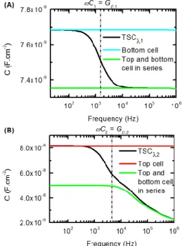
Figure 3: Simulated C-f curve when the TSC is under 0 V voltage bias and illuminated by a monochromatic light at a wavelength 1 (A) and 2 (B). Calculations
have been made for the TSC and for each subcell independently in their operating conditions in the TSC. (A), TSCλ1,black line), bottom cell in the dark and polarized at -VOC,1 (blue line), serial association of the
bottom cell (dark; -VOC,1) and the top cell (light-biased;
VOC,1) (green line); (B) TSCλ2 (black line), top cell in the dark and polarized at -VOC,2 (red line), serial
association of the top cell (dark; -VOC,2) (green line) and
the bottom cell (light-biased; VOC,2) . Dashed dotted
lines represent the frequency where 𝜔𝐶𝑖= 𝐺𝐷,𝑖.
Fig. 3 shows the capacitance versus frequency curves (C-f) that have been calculated when the TSC is under zero applied DC voltage and under a monochromatic light (1
or 2) with a photon flux in the range of 1 × 1015 cm-2.s -1. Additionally, each subcell has been simulated separately
in conditions corresponding to those in the TSC: when the TSC is illuminated at the wavelength 1 (2), calculations
are made for the top (bottom) cell alone under the same illumination conditions and at a forward bias close to its open-circuit voltage VOC,1 (VOC,2) and for the bottom (top)
cell alone in the dark at a reverse bias close to -VOC,1
(-VOC,2). Fig. 3A presents the results obtained under an
illumination at 1 for the TSC (TSC1), the bottom cell
alone and the serial association of the capacitance of the bottom cell alone and the top cell alone. Fig. 3B shows the equivalent calculations under an illumination at 2 with the C-f curve of the top cell alone instead of the bottom cell
alone. In the conditions of Fig. 3A, the depletion-layer capacitance CJ,2 ofthe bottom cell (lowly doped base) is in
the range of 10 nF.cm-2 while C
J,1 of the top cell (higher
doped base) is in the range of 100 nF.cm-2. Due to the low
Figure 2: (A) Equivalent circuit of the TSC in dark; (B) DC and (C) AC equivalent circuit of the TSC under reverse bias when the top cell is light-biased; (D) simplified AC equivalent circuit.
lifetime in the top cell, the diffusion capacitance CD,1 and
the diffusion conductance GD,1 are frequency independent
in the considered frequency range since 𝜔𝜏1≪ 1 and their
values can be estimated using Equations 4 and 7. The value of GD,1 is linked to the dark DC current at the operating
voltage of the cell, which can also be estimated from the short circuit current expected in this cell under light. For AM1.5 illumination, we would expect a value of about 0.8 S.cm-2 (corresponding to J
sc ≈ 20 mA cm-2 in a tandem
subcell), so for the much weaker monochromatic photon flux of 1 × 1015cm-2.s-1 used here, G
D,1 is of the order of
a few mS.cm-2 and C
D,1 = GD,1τeff is thus smaller than CJ,1.
The short transition in Fig. 3A thus occurs when ωCJ,1 ≈
GD,1, which is in the kHz range. Also, because C1 is
significantly larger than CJ,2, the two plateaus
corresponding to 𝐶𝐽,2 and 𝐶1𝐶𝐽,2
𝐶1+𝐶𝐽,2
are close one another. In Fig. 3B, the low frequency diffusion conductance GD,2 is
almost the same as GD,1 in Fig. 3A, because this value is
determined by the short circuit current of the light absorbing cell. However, due to the much larger effective minority carrier lifetime (≈1 ms) for the bottom cell, the diffusion capacitance CD,2 of the bottom cell is much larger
than its junction capacitance CJ,2 in the low frequency
range (LF). At high frequency (HF), CD,2 is frequency
dependent and decreases slowly as ω-1/2 (Eq. 3) so that the
total capacitance of the bottom cell saturates at CJ,2 at very
high frequency, and the tandem capacitance will then saturate at 𝐶𝐽,2𝐶𝐽,1
𝐶𝐽,2+𝐶𝐽,1, which is significantly smaller than CJ,1.
This explains the wider decrease of CTSC in Fig. 3B
compared to that of Fig. 3A, from 𝐶𝐽,1 to 𝐶𝐽,2𝐶𝐽,1
𝐶𝐽,2+𝐶𝐽,1 .
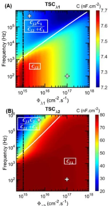
2.3 Photon flux dependency
All the physical quantities seen above (CJ, CD and GD)
are voltage bias dependent and therefore depend on the distribution of the applied voltage between both subcells. By considering the example given in Fig. 2B, the voltage in the bottom cell is 𝑉2= 𝑉𝐴𝑃𝑃− 𝑉𝑂𝐶,1. This means that
the photon flux (Φλi) has an influence on the distribution of the voltage in the TSC by changing the value of the open-circuit voltage of the light-biased cell:
𝑉𝑂𝐶,𝑖=𝑛𝑖𝑘𝑞𝐵𝑇× ln (𝑞×𝐸𝑄𝐸𝐽𝜆𝑖×𝛷𝜆𝑖
0,𝑖 ) (9)
where EQEλi is the external quantum efficiency at the considered wavelength λi, J0,i the saturation current in the
dark and ni the ideality factor of the light-biased (i-th)
subcell. Coupling Equation 9 with Equation 1 and 4 gives: 𝐶𝐽,𝑘= √ 𝑞𝜀𝑘 2(𝑉𝑏,𝑘−𝑉𝐴𝑃𝑃+𝑛𝑖𝑘𝐵𝑇𝑞 ×ln(𝑞×𝐸𝑄𝐸𝜆𝑖×𝛷𝜆𝑖𝐽0,𝑖 +1)−2𝑘𝐵𝑇/𝑞) ( 1 𝑁𝑏𝑎𝑠𝑒,𝑘+ 1 𝑁𝑒𝑚𝑖𝑡,𝑘) −1 (10) 𝐶𝐷,𝐿𝐹,𝑖= 𝑞2𝐸𝑄𝐸 𝜆𝑖×𝛷𝜆𝑖 𝑘𝐵𝑇 × 𝜏𝑒𝑓𝑓 (11) 𝐶𝐽,𝑖= √ 𝑞𝜀𝑖 2(𝑉𝑏,𝑖−𝑛𝑖𝑘𝐵𝑇𝑞 ×ln(𝑞×𝐸𝑄𝐸𝜆𝑖×𝛷𝜆𝑖𝐽0,𝑖 +1)−2𝑘𝐵𝑇/𝑞) (𝑁1 𝑏𝑎𝑠𝑒,𝑖+ 1 𝑁𝑒𝑚𝑖𝑡,𝑖) −1 (12)
The diffusion capacitance CD,i and the diffusion
conductance GD,i of the light-biased subcell are linear with
the photon flux while the depletion-layer capacitance has a much weaker increase. Considering the subcell in the
dark, its depletion-layer capacitance CJ,k decreases with
the increase of the photon flux absorbed by the light-biased subcell, due to a small negative shift of its operating voltage. Thus, the required condition on the frequency to have CTSC = CJ,k (see Fig. 3) changes with the photon flux.
Considering that the transition observed in Fig. 3 occurs at a pulsation ωc such as ωc Ci ≈ GD,i one can write in the low
frequency range (ωcτeff < 1):
𝜔𝑐= 𝐶𝐷,𝐿𝐹,𝑖 𝐶𝐷,𝐿𝐹,𝑖+𝐶𝐽,𝑖× 1 𝜏𝑒𝑓𝑓,𝑖 (13) which holds if 𝐶𝐷,𝐿𝐹,𝑖< 𝐶𝐽,𝑖. By inserting Equation 11 and
Equation 12 in Equation 13, we obtain a quasi-linear dependency of 𝜔𝑐 on Φλi. This can be seen in Fig. 4A, describing the capacitance of the tandem in the frequency – photon flux space (C-f-Φ) when the top cell is light-biased. Indeed, the white line representing the evolution of 𝜔𝑐 follows a linear trend as predicted. If 𝐶𝐷,𝐿𝐹,𝑖> 𝐶𝐽,𝑖,
which holds if the bottom cell is light-biased owing to the much larger effective lifetime in the bottom cell compared to that in the top cell, we obtain:
𝜔𝑐= ( 𝐶𝐷,𝐿𝐹,𝑖 𝐶𝐽,𝑖 ) 2/3 ×𝜏1 𝑒𝑓𝑓,𝑖 (14)
This shown as the white line in Fig. 4B.
Figure 4: Mapping of the capacitance in the frequency - photon flux space (C-f-Φ) for (A) the TSCλ1 and (B) the TSCλ2. The black dashed lines represent the cutlines from which the curves of the TSC in Fig. 3 were obtained. The white lines highlight the evolution of the frequency value for which 𝜔𝐶𝑖= 𝐺𝐷,𝑖. The white
crosses show the conditions taken for Fig. 5.
Mott-Schottky plots have been simulated for both TSCλ1 and TSCλ2 cases. For each case, two sets of conditions were chosen: a first set of conditions (tagged as “g”) taken below the white line in Fig. 4 with the frequency
of the AC small-signal equal to 100 Hz and a photon flux equal to 1 × 1017 cm-2.s-1 and a second set of conditions
(tagged as “b”) taken above the white line with the frequency of the AC small-signal equal to 500 kHz and a photon flux equal to 1 × 1015 cm-2.s-1. Mott-Schottky
plots of TSCλ1 and of the bottom cell alone are compared in Fig. 5A. Similarly Mott-Schottky plots of TSCλ2 and of the top cell alone are compared in Fig. 5B. Both figures illustrate the influence of the chosen parameters (frequency and photon flux) which is much more pronounced in Fig. 5B. Actually, the relative errors on the extracted quantities (slope of the 1/C² (V) linear part to deduce the doping densities and intercept voltage to deduce built-in potential) for the b-conditions are given in Table 1. The errors are much more important for the TSCλ2
cell which can be explained by considering that the transition between 𝐶𝐽,𝑘 and
𝐶𝐽,𝑘𝐶𝑖
𝐶𝐽,𝑘+𝐶𝑖 is larger. This
demonstrates that, if considering a TSC with a high difference between the doping densities in the bases, care must be taken to measure the capacitance by fulfilling the required conditions (low frequency and high photon flux). Especially when the subcell with the lowest doped base is light-biased.
Figure 5: Mott-Schottky plots from numerical calculations of 1/C2 values deduced from our
simulations of (A) the bottom cell alone in the dark (blue line), the TSCλ1 when the required conditions are met (black dots) or not (black line) and (B) the top cell alone in the dark (red line), the TSCλ2 when the required conditions are met (black dots) or not (black line). Table I: The relative errors of the extracted parameters from Mott-Schottky plots of the TSCλ1 and TSCλ2
simulated with a set of conditions that does not match the requirements. TSCλ1 (w) TSCλ2 (w) Slope 4.7 % 54.2 % Vint 10.7 % 148.6 % 3 APPLICATION 3.1 Required conditions
In order to experimentally validate our method, we have used an AlGaAs/Si TSC that was fabricated using doping densities in the range of 1 × 1015 cm-3 and
1 × 1017 cm-3 for the base of the Si and AlGaAs cells,
respectively, and corresponding emitter doping densities of 1 × 1020 cm-3 and 1 × 1018 cm-3 (see Reference [15])
for details of the structure and fabrication procedure). The capacitance-voltage measurements were performed using a HP4284A LCR-meter with a AC small-signal of 20 mV. The AlGaAs/Si tandem cell (0.5 × 0.5 cm2) was
illuminated by monochromatic light coming from a laser either at λ1=405 nm or at λ2=980 nm. These wavelengths
were chosen since according to the EQE [15],they are predominantly absorbed by one of the subcells. The 405 nm wavelength is absorbed by the AlGaAs top cell such that the capacitance of the Si bottom cell can be probed. In the same way, the 980 nm wavelength is absorbed in the Si bottom cell allowing us to probe the AlGaAs top cell.
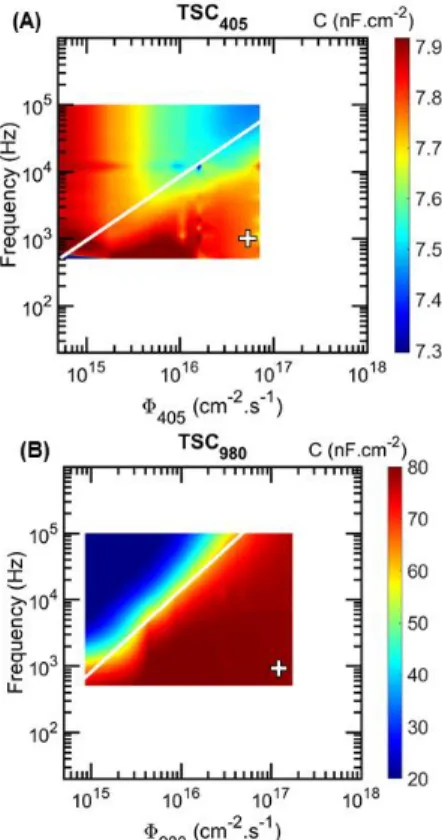
Figure 6: (A) Measured C-f-Φ405 mapping for the
TSC405 and (B) Measured C-f-Φ980 mapping for the
TSC980. White lines represent the limit where
𝜔𝐶𝑖~ 𝐺𝐷,𝑖. To emphasize the good agreement between
measurements and modeling, the axe limits are defined in order to match those of Fig. 4. The white crosses show the chosen experimental conditions.
Firstly, we present in Fig. 6, the measured C-f-Φ mapping of the TSC at 0 V for both wavelengths to find the best experimental conditions. We have limited the frequency range to 500 Hz – 100 kHz due to the increasing noise below 500 Hz and to circuit contributions above 100 kHz. The photon flux range is limited by the range of the two light biases from 1 mW up to 200 mW. However, in order to compare the global shape of the simulated C-f-Φ mapping with the measured ones, the X and Y axes in Fig. 6 are kept similar to that in Fig. 4. This highlights a good agreement between the simulations of the C-f-Φ mapping
and the measured one. Based on Fig. 6 we chose the frequency of the AC small-signal at 1 kHz and the photon flux at 5.3 × 1016 cm-2.s-1 and 1.3 × 1017 cm-2.s-1 for the
405 nm light bias and the 980 nm light bias, to extract parameters of the bottom cell and top cell, respectively. 3.2 Voltage shift and radiative coupling
As shown in section 2, the voltage bias in the subcell in the dark is 𝑉𝑘= 𝑉𝐴𝑃𝑃− 𝑉𝑂𝐶,𝑖. In order to access the C-V curve of the subcell of interest, measurements have to be
shifted by the open-circuit voltage of the illuminated cell. The open-circuit voltage is measured between the two terminals of the illuminated TSC when zero current is applied. In so doing, the subcell in the dark will be at 0 V while the illuminated cell will be at its open-circuit voltage value.
Figure 7: (A) Overestimated TSC405 voltage shift
measured when the Si bottom cell is in dark condition (circles) compared with the correct TSC405 voltage shift
measured when the Si bottom cell is strongly illuminated (dots). (B) Comparison between the Vint
value of the TSC405 Mott-Schottky plots after voltage
correction. Circles represent the underestimated value when shifting with the VOC measured when the Si
bottom cell is in dark condition while the dots represent the values when shifting the Mott-Schottky plots with the correct VOC value.
However, due to radiative recombinations, it is possible that the illuminated cell emits a small amount of light at an energy equal to its bandgap energy. In a TSC, the other subcell may absorb this emission if its bandgap energy is lower than the energy of the emitted photons from the other cell, which is likely to occur only when the top cell is light-biased. Thus, when measuring VOC,1 when
the top subcell is light-biased, the bottom cell is not completely in the dark and will contribute to the measured voltage. The voltage shift of the C-V curve will be
overestimated and the intercept voltage obtained when extrapolating the Mott-Schottky plot to zero, will then be underestimated. In order to highly decrease the impact of the radiative coupling on the measurement of the open-circuit voltage of the top cell, we first applied a high photon flux (1.8 × 1017 cm-2.s-1) at 980 nm absorbed by
the Si bottom cell and we measured VOC,2 of the bottom cell
(not influenced by radiative coupling). Then we added the TSC light-bias at 405 nm. Because of the logarithmic dependence of VOC on the photon flux, if a small amount
of light due to the radiative coupling is added to the high 980 nm photon flux on the bottom cell, it will not have a significant impact on the bottom cell contribution. The measured voltage can now be assumed to be the sum of
VOC,1 and the known VOC,2 and it is possible to determine
the top cell contribution alone. In Fig. 7A, the evolution of the overestimated VOC,1 and the correct values with the
photon flux are presented. Those values are used to shift the Mott-Schottky plots for different photon fluxes and to extract the intercept voltage represented in Fig. 7B. Both correct and underestimated Vint values first decrease due to
the proximity of the experimental condition with the transition zone where 𝜔𝐶2~ 𝐺𝐷,2. However the correct Vint
value becomes constant which proves that the impact of the radiative coupling has been strongly limited.
3.3 Parameters extraction
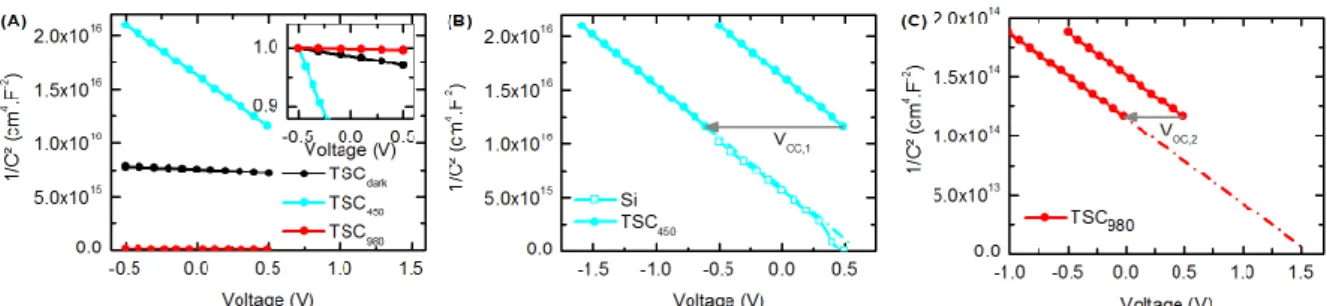
Finally, experimental Mott-Schottky plots of the TSC in the dark and under illumination are compared in Fig. 8A and it can be seen that the slopes are very different for each type of illumination and in the dark. In Fig. 8B, the Mott-Schottky plot of the capacitance of the TSC405 is compared
with measurements performed on a tandem where the top subcell has been short-circuited resulting in an isotype Si cell. The alignment of both curves after the voltage shift indicates that, using the proposed method, we successfully probed the Si bottom subcell of the TSC. Doping densities in the base of the Si bottom subcell of the TSC and of the isotype Si cell have been determined according to Equation 2 taking account of the relative dielectric permittivity of silicon (11.7). Doping densities in the p-type base and the built-in potentials are summarized in Table 2. Small differences between values can be explained by measurement uncertainties or by slight variations in the fabrication process from one cell to the other. Similarly, the Mott-Schottky plot of the TSC980 is
shifted by the open-circuit voltage of the bottom subcell in Fig. 8C. The doping density in the emitter cannot be neglected and has been considered in Equation 1 when extracting the density in the base with a relative dielectric permittivity value taken equal to εs,1=12.28. No isotype
AlGaAs cell was available to compare with the TSC980 but
the calculated Nbase,1 value can be compared with the value
targeted during the fabrication process which is in the same range. The results summarized in Table 2 allow us to validate the proposed method. Indeed, we obtain a very good agreement between the extracted properties of the subcells of the TSC, those of the isotype Si cell and those targeted during the fabrication process. In addition, it should be emphasized that the method enables to extract doping densities in the base of subcells even if they are very different (more than a factor of 100 in our TSC).
Figure 8: Experimental Mott-Schottky plots: (A) 1/C2curves of the AlGaAs/Si TSC in the dark (black line with dots), under
a 405nm (blue line with dots) and a 980 nm light bias (red line with dots). Inset: normalized 1/C2, curves are shifted to the
value of the TSC980 at V = -0.5 V and normalized to 1 to emphasize that the average slope for the TSC in the dark is different
from those under illumination. (B) 1/C2curve of the TSC
405 (lines with dots) are shifted by the open-circuit voltage of the
top subcell and compared with an isotype Si cell (line with square symbols) to show that the Si bottom subcell of the TSC has been probed. (C) 1/C2 curve of the TSC
980 (lines with dots) are shifted by the open-circuit voltage of the bottom subcell.
Table II: Doping density (Nbase,i) in the base, build-in
potential (Vb,i) extracted from Mott-Schottky plots of
the TSC405, the TSC980 and the isotype Si cell are
compared with targeted doping density values based on the values given in Reference [15] and with expected built-in voltage values based on modeling of targeted the structure.
Nbase,i [cm-3] Vb,i [V]
Targeted for Si 1 × 10¹⁵ 0.69
Measured from Si isotype 1.3 × 10¹⁵ 0.69
Measured from TSC405 1.3 × 10¹⁵ 0.69
Targeted for AlGaAs 1 × 10¹⁷ 1.59
Measured from TSC980 1.7 × 10¹⁷ 1.66
4 CONCLUSION
In conclusion, we have presented a method in order to extract key parameters of individual subcells in a tandem solar cell (doping density in the base and potential barrier height) from capacitance measurements performed on the tandem cell under specific light-biasing conditions. Using both analytical and numerical modeling approaches, we have developed a comprehensive analysis of the capacitance response of the tandem solar cell, and detailed the influence of the flux of the light-bias and of the measurement frequency. We have shown that the diffusion conductance and the diffusion capacitance play an essential role, since they allow to screen the contribution of the light-biased cell to the tandem capacitance. Low frequency and high photon flux should be privileged for extracting parameters in a III-V/Si TSC. The method has been applied to an AlGaAs/Si TSC. Experimental results are well described by our analysis. The parameters extracted from measurements on the TSC are in good agreement with that obtained from isotype cells, and also with the values targeted in the AlGaAs/Si process. The proposed method is simple and non-destructive, and can be extended to other multijunction cells and to other capacitance-based characterization techniques such as admittance spectroscopy by integrating the contribution of defects to the analysis.
5 REFERENCES
[1] Fan JCC, Tsaur B-Y, Palm BJ. In: 16th Photovolt.
Spec. Conf. New York: IEEE; 1982. 692-701.
[2] Richter A, Hermle M, Glunz SW. Reassessment of the limiting efficiency for crystalline silicon solar cells. IEEE J. Photovoltaics 2013. 3(4): 1184-1191.
[3] Yu Z, Leilaeioun M, Holman Z. Selecting tandem partners for silicon solar cells. Nat. Energy 2016. 1(11): 16137.
[4] Essig S, Allebe C, Remo T, Geisz JF, Steiner MA, Horowitz K, Barraud L, Ward JS, Schnabel M, Descoeudres A, Young DL, Woodhouse M, Despeisse M, Ballif C, Tamboli A. Raising the one-sun conversion efficiency of III-V/Si solar cells to 32.8% for two junctions and 35.9% for three junctions. Nat. Energy 2017. 2: 17144.
[5] Meusel M, Baur C, Siefer G, Dimroth F, Bett AW, Warta W. Characterization of monolithic III-V multi-junction solar cells – challenges and application. Sol. Energy Mater. Sol. Cells 2006. 90(18-19): 3268-3275.
[6] Ruiz CM, Rey-Stolle I, Garcia I, Barrigon E, Espinet P, Bermudez V,Algora C. Capacitance measurements for subcell characterization in multijunction solar cells. In 35th IEEE Photovolt.
Spec. Conf. IEEE; 2010. 708-711.
[7] Hoheisel R, Schachtner M, Stämmler E, Bett AW. Determination of the subcell photovoltage in multijunction solar cells via voltage-dependent capacitance analysis. Appl. Phys. Lett. 2011.98(25): 251106.
[8] Rutzinger M, Salzberger M, Gerhard A, Nesswetter H, Lugli P, Zimmermann CG. Measurement of subcell depletion layer capacitances in multijunction solar cells. Appl. Phys. Lett. 2017. 111(18): 183507. [9] Hillbrand J, Gold RD. Determination of the impurity distribution in junction diodes from capacitance - voltage measurements. RCA Rev. 1960. 21: 245-252. [10] Lang DV. Deep-level transient spectroscopy: a new method to characterize traps in semiconductors. J.
Appl. Phys. 1974. 45(7): 3023-3032.
[11] Losee DL. Admittance spectroscopy of impurity levels in Schottky barriers. J. Appl. Phys. 1975. 46(5): 2204-2214.
[12] Peaker AR, Markevich VP, Coutinho J. Tutorial: junction spectroscopy techniques and deep-level defects in semiconductors. J. Appl. Phys.2018. 123(16):161559.
[13] Silvaco, Atlas User’s Manual, 2016.
[14] Sze SM. Physics of Semiconductor Devices, 2nd edition ed. John Wiley & Sons, Murray Hill, New Jersey: Wiley-Interscience; 1981.
[15] Vauche L, Veinberg Vidal E, Jany C, Morales C, Decobert J, Dupre C, Mur P. 33rd Eur. Photovolt.