HAL Id: tel-01775272
https://tel.archives-ouvertes.fr/tel-01775272
Submitted on 24 Apr 2018HAL is a multi-disciplinary open access archive for the deposit and dissemination of sci-entific research documents, whether they are pub-lished or not. The documents may come from teaching and research institutions in France or abroad, or from public or private research centers.
L’archive ouverte pluridisciplinaire HAL, est destinée au dépôt et à la diffusion de documents scientifiques de niveau recherche, publiés ou non, émanant des établissements d’enseignement et de recherche français ou étrangers, des laboratoires publics ou privés.
Strain relaxation in InGaN/GaN herostructures
Quantong Li
To cite this version:
Quantong Li. Strain relaxation in InGaN/GaN herostructures. Theoretical and/or physical chemistry. Normandie Université, 2018. English. �NNT : 2018NORMC204�. �tel-01775272�
Strain relaxation in InGaN/GaN heterostuctures
THESE
THESE
Pour obtenir le diplôme de doctorat
Spécialité CHIMIEPréparée au sein de l’ENSICAEN et l’UNICAEN
Présentée et soutenue par
Quantong LI
Thèse soutenue publiquement le 20/03/2018 devant le jury composé de
Madame Sabine LAY Directeur de Recherche CNRS
Université Grenoble Alpes Rapporteur
Monsieur Ludovic DESPLANQUE Maitre de Conférences HDR
Université Lille 1 Rapporteur
Monsieur Olivier PEREZ Directeur de Recherche CNRS
ENSICAEN Examinateur
Monsieur Piero GAMARRA Ingénieur, Thales research and technology Examinateur
Monsieur Jun CHEN Professeur des Universités
Université de Caen Normandie Co-Directeur de thèse
Monsieur Pierre RUTERANA Directeur de Recherche CNRS
ENSICAEN Directeur de thèse
Acknowledgements
The work has been carried out at CIMAP laboratory along these three years. Behind this achievement, there are a great many people, who gave me help, support and inspiration so that make it possible and therefore I take this opportunity to express my special gratitude to all of you for contributing to my thesis.
I first express deep gratitude to my supervisor Dr. Pierre Ruterana for giving me the opportunity to carry out my PhD Research work and for leading me into the field of transmission electron microscopy and defects. Over the past three years, he has given me guidance, support, and encouragements for my research. I express greatest thanks to Prof. Jun Chen, my co-supervisor for encouraging me to spend more time in my research. It is a pleasure for me to thank Dr. Sabine Lay and Dr. Ludovic Desplanque for having accepted to review my manuscript. In the same vein, my acknowledgements go also to Dr. Olivier Perez and Dr. Piero Gamarra for having accepted to judge my work as members of the examination committee.
I am very much grateful to Dr. Albert Minj for rekindling my interests in crystallography, semiconductor physics, nanotechnology and proving that learning can be fun, and he has always been a source of encouragement.
Finally, my gratitude goes to my colleagues in PM2E TEM, Marie-Pierre Chauvat for teaching and helping me with sample preparation and Hichem Ben Ammar for all the good discussions in research and life.
To all my friends in Caen for making my life colorful all along these three years. And above all to my parents, for endless love and support.
During this work, I benefited from a financial grant provided by the China Scholarship Council
CONTENTS
Résumé ... I
Introduction ... VII
Chapter 1 ... 1
The III-nitride semiconductors ... 1
1. 1 Introduction ... 2
1. 2 Properties of group III nitrides ... 4
1. 2. 1 Crystalline structure ... 4
1. 2. 2 Crystal polarity ... 7
1. 2. 3 Dislocations ... 8
1. 3 Group III nitrides epitaxy ... 10
1. 3. 1 Substrates for group III nitrides ... 11
1. 3. 2 Sapphire substrate ... 12
1. 3. 3 SiC ... 12
1. 3. 4 Si ... 13
1. 4 Slip systems in hexagonal materials ... 13
1. 5 Applications of group III nitrides ... 15
1. 5. 1 Optical applications ... 16
Chapter 2 ... 25
Experimental techniques ... 25
2. 1 Metal Organic Vapor Phase Epitaxy (MOVPE) ... 26
2. 2 Molecular Beam Epitaxy (MBE) ... 28
2. 3 The investigated samples ... 29
2. 4 Microscopy techniques ... 30
2. 4. 1 Atomic Force Microscopy (AFM) ... 30
2. 4. 2 Transmission Electron Microscopy (TEM) ... 33
2. 5 TEM specimen preparation ... 39
2. 5. 1 Shaping the samples ... 40
2. 5. 2 Thickness reduction by mechanical polishing ... 41
2. 5. 3 Ion polishing ... 42
Chapter 3 ... 45
Metal Organic Vapor Phase Epitaxy of InGaN/GaN heterostructures ... 45
3. 1 Introduction ... 46
3. 2 The samples ... 47
3. 3 Structural analysis of MOVPE layers ... 48
3. 3. 1 The surface morphology by AFM ... 48
3. 3. 2 Microstructural analysis ... 52
Chapter 4 ... 65
Plasma Assisted Molecular Beam Epitaxy of In-rich InGaN/GaN heterostructures ... 65
4. 1 Introduction ... 66
4. 2 PAMBE growth of InGaN layers ... 67
4. 3 The surface morphology ... 68
4. 4 The microstructure analysis ... 70
4. 5 Discussion and Conclusion ... 78
Chapter 5 ... 81
The interface dislocations in the InGaN/GaN heterostructures ... 81
5. 1 Introduction ... 82
5. 2 Low misfit (In < 10%) ... 83
5. 3 Intermediate (In ~ 13%) ... 84
5. 4 Medium misfit (In ≥ 18%) ... 86
5. 5 High misfit (In ~ 30%) ... 86
5. 6 Discussion ... 88
5. 7 Summary ... 92
Chapter 6 ... 95
I
II
Les semi-conducteurs nitrures (AlN, GaN, InN) et leurs alliages font l'objet d'intenses recherches depuis bientôt 30 ans. Les propriétés physiques des composés binaires et des alliages de nitrures du groupe III les rendent tout à fait indispensables dans les domaines de l'électronique et de l'optoélectronique. Par exemple, les alliages InGaN sont utilisés pour fabriquer des diodes électroluminescentes, des diodes laser, des transistors et des cellules solaires. Cependant, en raison de la décomposition spinodale susceptible de se produire dans l'alliage InGaN, des phénomènes induits chimiquement, tels que la séparation des phases, la mise en ordre à longue distance ont été rapportés, cela conduit à des couches affichant des microstructures avec défauts complexes. L’autre défi avec l'hétérostructure InGaN/GaN est la relaxation de la contrainte à l'hétérointerface. En raison du décalage paramétrique entre la couche épitaxiale InGaN et le GaN, de nombreux défauts sont présents dans la couche InGaN, par exemple des défauts en V, des dislocations et des fautes d'empilement, mais aussi des dislocations dans l'interface pendant la croissance. Comme les défauts se forment en fonction de la composition en l'indium et de l'épaisseur de la couche, le but de ce travail a été de comprendre les mécanismes de relaxation des contraintes présentes afin d'aider à la croissance des couches de meilleure qualité cristalline pour la possible fabrication de dispositifs performants.
Cette thèse porte sur une étude détaillée de la morphologie de surface et de la microstructure des couches InGaN/GaN obtenues par épitaxie en phase vapeur aux organométalliques (EPVOM) et aussi par l'épitaxie aux jets moléculaires assistée par plasma (EJM) en utilisant la microscopie à force atomique (AFM) et ensuite la microscopie électronique à transmission (MET). Le but est de mettre en évidence la relation entre le type de défaut et la relaxation des contraintes dans les hétérostructures InGaN/GaN.
III
Chapitre 1 : Les semi-conducteurs nitrures de métaux du groupe III
Dans le chapitre 1, nous présentons les semi-conducteurs de nitrure, leur structure cristalline, la polarité, les défauts cristallins, les substrats de croissance des nitrures du groupe III, la relaxation de la contrainte aux interfaces ainsi que leurs applications dans l'électronique et l'optoélectronique.
Chapitre 2 :Techniques expérimentales
Au cours du chapitre 2, nous avons décrit les techniques de croissance EPVOM et EJM utilisées pour croître les couches analysées au cours de ce travail de thèse. Les échantillons d’InGaN/GaN/saphir ont été obtenus par EPVOM grâce à nos collaborations avec AIXTRON et l'École Polytechnique Fédérale de Lausanne, Suisse. Les couches EJM ont été fabriquées à l’INAC, Grenoble. Les informations quantitatives sur la morphologie de surface des échantillons en termes de rugosité ont été obtenues par AFM. Dans cette étude, la partie la plus importante de MET a été réalisée sur un microscope JEOL JEM-2010 fonctionnant à une tension d'accélération de 200 kV en utilisant une source thermoionique d'hexaborure de lanthane (LaB6). Un MET à
haute résolution de 200 kV avec une résolution maximale de 0.19 nm (Cs = 1.4 mm pour
HAADF) a également été utilisé dans notre étude pour l'imagerie à haute résolution et l’analyse locale par spectroscopie aux rayons X (EDS). La diffraction X a été aussi utilisée dans cette étude pour une analyse de la qualité cristalline des couches principalement riches en indium obtenues par EPVOM.
Chapitre 3 : Couches d’InGaN par EPVOM
Ce chapitre est focalisé sur la détermination du rôle de la concentration d'indium que nous avons fait varier entre 4% et 100% sur la relaxation des contraintes. Nous avons étudié la morphologie de surface et la microstructure des couches InGaN obtenues par MOVPE en utilisant d’abord l’AFM et ensuite la MET. Nous avons trouvé que la morphologie de surface
IV
dépend fortement de la composition en In. Pour x < 0.13, les surfaces présentent des marches atomiques, avec une très faible densité de défauts en V. Entre 0.13 ≤ x ≤ 0.18, les surfaces contiennent un réseau plus ou moins hexagonal de défauts linéaires dont la densité croît avec la concentration en indium. Au-delà d’une composition de 25%, le mode de croissance 3D devient prédominant. Par MET, les résultats montrent qu'il n'y a pas de dislocations dans les hétérostructures InGaN/GaN pour la plus faible concentration en In. Pour 0.13 ≤ x ≤ 0.25, les dislocations traversantes et les défauts en V sont systématiquement présents dans InGaN, les dislocations de décalage paramétrique en grande densité sont observées lorsque la concentration en In devient supérieure à 0.18. On peut de plus avoir formation des défauts d’empilement dans les couches pour In = 25% en étroite interaction avec les défauts en V. Au-delà de 40% en In, il y a une forte croissance 3D, et une dégradation très rapide de la qualité cristalline des couches d’InGaN jusqu’à contenir une forte porosité.
Chapitre 4 : Couches d’InGaN obtenues par EJM
Le principal avantage de la croissance par EJM est que nous avons pu avoir des couches de InGaN épaisses (jusqu’à 500 nm) ayant une faible rugosité de surface. Nous avons donc pu nous attacher à étudier en détail les mécanismes qui peuvent intervenir pour la relaxation de la contrainte, en effet, le seul paramètre qui était censé varier d’un échantillon à l’autre était l’épaisseur, la composition nominale ayant été voulu constante à 30% d’indium. Ainsi, à l’épaisseur la plus faible de la couche d’InGaN, il n’y pas de formation de défauts, ni dans la couche, ni dans l’interface, elle est donc contrainte sur le GaN. Cependant, dès 30 nm d’épaisseur, la couche montre une formation de fautes d’empilement au niveau de l’interface, avec certaines qui peuvent aller jusqu’en surface. Lorsque l'épaisseur de la couche est supérieure à 80 nm, les dislocations de décalage paramétrique sont déjà en forte densité dans l’interface, des demi-boucles de dislocation partent alors de la surface vers l’interface, et la couche contient de
V
nombreuses fautes d’empilement. A l’épaisseur la plus grande étudiée (500 nm), l’interface InGaN contient les dislocations de décalage paramétrique, qui, bien que très nombreuses, ne sont pas suffisantes pour relâcher toute la contrainte. En effet, de très fortes densités de dislocations traversantes sont présentes ainsi que des demi-boucles de dislocations qui descendent de plus en plus auprès de l’interface. De plus, la couche de surface est très perturbée : les séquences de l’empilement hexagonal ont été perdues, et la composition en surface s’est enrichie en indium par rapport au volume.
Chapitre 5 Formation de dislocations dans l’interface InGaN/GaN
Dans nos échantillons, la composition en In varie de 4 à 100%, et donc le décalage paramétrique lors de la croissance sur (0001) GaN est compris entre 1 et 11.3%. Dans ces matériaux hexagonaux, la relaxation de la contrainte d'interface durant la croissance épitaxiale n'est pas bien connue et on s'attend à ce qu'elle se déroule de manière différente de ce qui se passe dans le système cubique. En particulier, la croissance le long de la direction [0001] limite le glissement des dislocations sur seulement quelques familles de plans atomiques. Fait intéressant, ce travail permet de montrer que cette relaxation suit plusieurs chemins. En effet, lorsque la composition en indium est de l'ordre de 10%, aux épaisseurs des couches que nous avons étudiées, on s'attendrait déjà à la formation de dislocations de décalage paramétrique. Cependant, notre étude montre que ce sont des dislocations vis qui sont présentes à l'interface InGaN/GaN. De plus, en dessous de 18% de composition d'indium, ces dislocations vis coexistent avec des dislocations coins de décalage paramétrique. Outre les dislocations de rattrapage du décalage paramétrique, d'autres mécanismes ont été mis en évidence pour la relaxation des contraintes. En effet, au-dessus d'une composition d'indium supérieure à 25%, de nombreux phénomènes se produisent simultanément : (1) formation des dislocations coins à l'interface; (2) enrichissement en indium en surface par rapport au volume de la couche d’InGaN;
VI
(3) disparition de la séquence hexagonale vers la surface conduisant à un empilement aléatoire;
(4) croissance 3D pouvant même conduire à des couches poreuses lorsque la composition en indium est comprise entre 40% et 85%.
Chapitre 6 Conclusion générale et perspective
Ce chapitre résume les principaux résultats obtenus et discutés dans les chapitres 3 à 5 en soulignant les contributions originales que l’étude comparative de matériaux obtenus par deux méthodes de croissance différentes nous ont permis de faire sur une connaissance des mécanismes de relaxation des hétérostructures InGaN/GaN. L’analyse des couches obtenues par EJM jusqu’à de fortes épaisseurs nous a montré pour la première fois la forte contribution des dislocations mixtes ‘a + c’ dans la formation des dislocations a coins de décalage paramétrique. Les analyses en section plane du chapitre 5 montrent aussi la présence de dislocations a vis aux faibles teneurs en indium. Ces deux résultats très intéressants demandent un travail encore plus approfondi pour bien comprendre les mécanismes sous-jacents. En effet, si le réseau de dislocations vis apparait d’abord, comment se transforme-t-il en dislocations coins qui seules peuvent aider à relâcher la contrainte due au décalage paramétrique. En ce qui concerne le glissement des dislocations mixtes, nos analyses menées en section plane ne permettent pas d’indiquer ce que devient la composante c lorsque la demi boucle atteint l’interface InGaN/GaN pour donner naissance à la dislocation a coin, il faut donc poursuivre les travaux pour pouvoir conclure.
VII
VIII
The nitride semiconductors (AlN, GaN, InN) and their alloys have become a subject of intense investigation during the last 30 years. Their properties make them exclusive for applications in the fields of electronics and optoelectronics, for instance, InGaN-based alloys are used to fabricate light-emitting diodes (LEDs), laser diodes (LDs), transistors as well as solar cells. These applications are based on heterostructures of these compounds and their ternary alloys. Still, the fabrication of optimized devices remains a challenge due to many yet non-solved issues. Indeed, the three compounds exhibit substantial differences in physical properties such as lattice and thermal mismatch, growth temperature, etc. This is at the origin of possible spinodal decomposition of some of the ternary alloys which leads to chemically induced phenomena, such as phase separation, ordering and compositional pulling, which have been reported depending on the growth conditions. The other challenge for the InGaN/GaN heterostructures, where the lattice mismatch between GaN and InN is up to 11%, is the relaxation of the strain at the heterointerface. As a consequence, high densities of defects can be generated in the InGaN layers, depending on the growth conditions, for example, V-shaped defects, dislocations, stacking faults, with the inherent subsequent degradation of the devices. At the heterointerface, it is expected that misfit dislocations form depending on the indium composition and the layer thickness. The objective of this work has been to determine the strain relaxation mechanisms of the InGaN alloys grown on GaN in order to assist in the growth of best crystalline quality layers for device applications.
This thesis relates a detailed research on the surface morphology and the strain relaxation of the InGaN layers on GaN templates grown by Metalorganic Vapour Phase Epitaxy (MOVPE) as well as Plasma Assisted Molecular Beam Epitaxy (PAMBE), the purpose is to point out the relationship between the defect type and the strain relaxation.
IX semiconductors.
Chapter 2 gives a description of the growth, the preparation as well as the characterization techniques used for investigating the samples.
Chapter 3 details the results of our systematical study of the surface morphology and the cross-sectional microstructure of the InGaN layers grown by MOVPE using Atomic Force Microscopy (AFM) as well as Transmission Electron Microscopy (TEM).
Chapter 4 focuses on investigating the influence of varying layer thickness on strain relaxation. We analyzed the surface morphology and the cross-sectional microstructure of the InGaN layers grown by PAMBE respectively using AFM and TEM. The main results obtained in this study allow determining the dominant strain relaxation processed in InGaN layers grown on GaN, they include composition fluctuation, composition pulling at large thicknesses and the hexagonal stacking disruption during the growth.
Chapter 5 reports our detailed analysis of the relaxation of the heterostructures as a function of indium composition by the generation of misfit dislocations. It is shown that the formation of dislocations could start at an indium concentration of around 10% with the generation of screw dislocations, by 13%, we point out a mixed network of edge and screw dislocations up to 17%, and past 18%, only a dense network of a type edge dislocations are generated with their lines along <101̅0> directions.
Chapter 6 summarizes the general conclusion of this work and discusses some of the open questions.
1
Chapter 1
2
1. 1 Introduction
Semiconductor-based devices have been successfully used in microelectronics, optoelectronics as well as chemical sensors. The nitride semiconductors, aluminum nitride (AlN), gallium nitride (GaN), and indium nitride (InN) as well as their alloys have become a subject of intense research during the last 30 years. For one material family, the have unique properties i.e., a wide direct bandgap, strong chemical bonds that make them suitable for the production of optoelectronic devices (both emitters and detectors) and high-power/temperature electronic devices, as have been reviewed many times in the literature [1-7].
It is now more than 100 years that the investigation of these materials started: the first synthesis of AlN, GaN as well as InN was reported in 1907 [8], 1910 [9], and 1932 [10], respectively. As these compounds do not exist as bulk materials, they need to be synthetized on various substrates. Although GaN was first synthesized a long time ago, the interest in this group of semiconductors was limited because of the extreme difficulties of growing them in single-crystalline form. This latter fact was attributed to their thermodynamic properties, for example, in the case of GaN, the melting temperature of 2500 °C is quite high and is accompanied by a high equilibrium nitrogen pressure of ~45000 bar. In the period 1965-1975, Jacques Pankove and his students did pioneering work in growing as well as characterizing GaN [11]. Therefore, it took many decades to attain significant progress for the growth of GaN epitaxial layers on sapphire substrates using Hydride Vapor Phase Epitaxy (HVPE) [12], Metalorganic Vapor Phase Epitaxy (MOVPE) [13] or Molecular Beam Epitaxy (MBE) [14].
The breakthrough of nitrides took place in 1989 thanks to the Japanese scientists Amano, Akasaki, and Nakamura, who overcame the issues of growth and p-type doping [15, 16] which initiated the advent of violet to yellow light emitting diodes (LEDs) [17-19], laser diodes (LDs)
3
[18], UV LEDs [19, 20]. They used the MOVPE technique to grow nitride layers on sapphire substrates. They also used a post-growth activation process to achieve p-type material. From this time onwards, the development of this material was strongly driven by the industrial demand for LEDs and lasers. At present, blue and green LEDs as well as blue LDs are commercially available [21]. This was mainly because of their direct energy gaps covering the whole visible spectrum as well as a large part of the ultraviolet (UV) spectral region [22], extending from InN (0.7 ± 0.05 eV, near infrared) [23], to GaN (3.4 eV, mid UV), finally to AlN (6.2 eV, deep UV) [24]. Specifically, nitrides are suitable for such applications as surface acoustic wave devices [25], UV detectors [26, 27], Bragg reflectors [28], waveguides, UV and visible LEDs [29-31] as well as LDs [32] for digital data read-write applications.
From then, GaN and its alloys with AlN and InN have become the second important family of semiconductor materials just after silicon because they should allow the design and production of devices with unique electronic and optoelectronic properties [33-37]. The development of indium gallium nitride (InGaN) is one of the emerging field of research in III-nitrides [38]. The direct band gap of InxGa1-xN can be designed to emit light all over the visible spectrum
depending on the indium content (x) of the film. InGaN-based alloys are therefore used to fabricate LEDs, LDs [39, 40] as well as solar cells [41, 42]. InGaN alloys are excellent candidates for the light-absorption layers in solar cell applications due to their high-energy radiation resistance [41], and because InGaN alloys across the range of indium compositions absorb light over the whole solar spectrum in a multijunction solar cell [43]. On the other hand, however, the development of GaN-based technology was, and still is, strongly limited by difficulties in obtaining large, high quality GaN crystals. This is a direct consequence of thermodynamic properties of GaN [44] (and also AlN [45]). An additional effort has been made towards High Electron Mobility Transistors (HEMTs) based on nitride heterostructures [46], and
4
intense research has been dedicated towards the application of group III nitride materials in high power, microwave frequency electronic devices [47, 48]. GaN’s wide band gap, large dielectric breakdown field, and fortuitously good electron transport properties [49-51] as well as good thermal conductivity are trademarks of high-power/temperature electronic devices [52]. Several groups have reported on the superior performance of GaN-based modulation-doped FETs (MODFETs) on silicon carbide (SiC) and sapphire substrates with respect to competing materials, especially at X band and higher frequencies [53-56]. Applications of high-power GaN-based MODFETs include amplifiers operative at high power levels, high temperatures as well as in unfriendly environments such as radars, missiles, satellites, and in low-cost compact amplifiers for wire-less base stations.
1. 2 Properties of group III nitrides
1. 2. 1 Crystalline structure
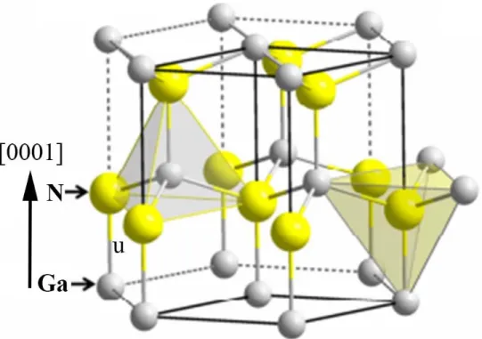
The three (Al, Ga, In) nitride compounds and their alloys are most stable in the wurtzite structure Figure 1.1 [57, 58], which consists of two hexagonal close packed sublattices of group III metal and nitrogen atoms, respectively, the corresponding space group is P63mc. The two
sublattices should be ideally related by a translation u = 3c/8 along [0001] c-axis and each atom is surrounded by four atoms of the other kind at the edges of a tetrahedron.
In a hexagonal system, the notation for the four indices (h k i l) is assigned to the three base vectors a1, a2, a3 and c respectively. The third index i is defined as, i = – (h + k) and the three ai
5
Figure 1.1 Illustration of atomic distribution in wurtzite lattice.
As can be seen in Figure 1.2, the band gap of group III nitride semiconductors can be adjusted in a wide range from near infrared (IR) to deep UV spectral region.
6
In the first approximation which is called “the Vegard law”, many properties (lattice parameters, band gaps, etc.) may be deduced from those of the end binary compounds. For instance, the band gap of a ternary alloy (e. g. AxB1-xN) may be deduced as:
aAB= xaA + (1 – x)aB (1. 1)
As the materials are grown as thin layers on substrates such as sapphire, SiC, Si, etc., residual strain build up as due to lattice, and thermal mismatch. The lattice mismatch is defined as:
= (as – al) / as (1. 2)
where as is the lattice parameter of the substrate, and al is the corresponding one for the
epitaxial layer. As can be seen in table 1.1, which exhibits the lattice parameters, important differences exist for the three nitride binary compounds in the wurtzite structure.
Table 1.1 Lattice parameters and mismatch of bulk InN, GaN and AlN at room temperature [58].
The other properties of wurtzite AlN, GaN and InN (electronic, thermal and optical, etc.) are also quite different (Table 1.2). In many instances, the growth of their heterostructures as well as alloys may not lead to good quality layers due to such large mismatch.
7
Table 1.2 Physical properties of III nitride materials [59-62].
1. 2. 2 Crystal polarity
The group III nitrides are not centrosymmetric crystal structures, as a result, the two crystallographic directions [0001] and [000-1] are not equivalent. Conventionally, the [0001] polarity is defined by the direction of the vector pointing from the metal (Al/Ga/In) atom to nitrogen (N) along the <0001> axis as shown in Figure 1.3. An epitaxial layer grown along this direction is called metal polar and the material grown in the opposite direction is called nitrogen polar. The two different polar materials possess distinct properties in terms of surface morphology, chemical reactivity, thermal stability and even the growth conditions. For instance, metal-polar surfaces have been reported to present a higher chemically stability than nitrogen polar surfaces [63, 64].
8
Figure 1.3 Metal polar surface of wurtzite nitrides are mainly terminated by metallic atoms [65]. The selection between the two polarities during the epitaxial growth of this Group III nitride system i.e. metal polar or N-polar, depends on the used substrate material and the growth conditions [66]. The polarity of the films can be probed by various techniques like wet chemical etching, electron microscopic techniques such as Convergent Beam Electron Diffraction (CBED), Co-Axial Impact Collision Ion Scattering Spectroscopy (CAICISS). More recently hydrogen irradiation has also been proposed to be effectively sensitive to the polarity [63].
1. 2. 3 Dislocations
Dislocations are linear defects which are some of the typical imperfections in the crystalline structure. They are generated to relax the stress which may arise during the growth and any other mechanical deformation in order to decrease the global energy of the material system. If formed during an epitaxial growth, they originate from the difference of lattice parameters and thermal expansion coefficients of the substrate and the epilayer. These linear defects are characterized by their Burgers vector b and dislocation line u. Depending on their density inside the layers used for the fabrication of electronic components, they strongly affect
9 the device performance [67, 68].
In group III nitride epitaxy, the most common dislocations are the threading Dislocations (TDs) [69, 70] which are generated at the interface with the substrate and propagate up to the surface of the layer, through the active part of the component. A dislocation can either be perfect or partial. A dislocation is said to be perfect, when its Burgers vector corresponds to an entire translation of the lattice; it is partial when the Burgers vector is a fraction of a translation of the lattice. In nitride layers grown along c, the main defects are TDs (shown in Table 1.3), which form as edge, screw or mixed type and are distinguished by the angle made between the Burgers vector and the dislocation line.
(1) For a pure edge dislocation, the dislocation line is perpendicular to Burgers vector b. A schematic diagram of atomic planes can be used to illustrate lattice defects such as dislocations. The "extra half-plane" concept of an edge type dislocation is shown in Figure 1.4.
(2) For a screw dislocation, the dislocation line is parallel to the Burgers vector as shown in Figure 1.4.
(3) For a mixed type dislocation, there is no defined angular relationship between the dislocation line and the Burgers vector.
10
Table 1.3 Perfect and partial dislocations in group III nitride epitaxial layers grown along the [0001] direction [68, 69].
1. 3 Group III nitrides epitaxy
The common growth techniques for III nitrides are Hydride Vapor Phase epitaxy (HVPE), Metal organic Vapor Phase epitaxy (MOVPE), Molecular beam epitaxy (MBE). Among them MOVPE and MBE are the most used for device processing and they were employed to grow the samples which are investigated in this work.
The quality of epitaxial layers depends upon the growth technique, the epitaxial growth mode (homoepitaxial or heteroepitaxial), the substrate used and the growth conditions. The choice of growth technique depends on the desired structure and applications. For example, in case of industrial production, MBE had less success for nitrides than MOVPE. For group III nitrides growth, although bulk GaN and AlN are available, the small size and high cost prevent their wide usage. Therefore, due to the current lack of affordable bulk nitride substrates, group III nitrides are grown by heteroepitaxy. Lattice and thermal mismatch between epitaxial layers and substrates have long been the major challenge in obtaining high quality devices in the III-Nitride material system. The properties of the most commonly used substrates for group III
11
nitrides are listed in Table 1.4, which indicates a large lattice and thermal mismatch between the III-nitrides and the substrates. Because of this mismatch the growth of good quality epilayers is challenging.
Table 1.4 Properties of substrates for III-Nitride growth [61, 62, 72].
1. 3. 1 Substrates for group III nitrides
For epitaxial growth, one of the major issues is to select the suitable substrate. Generally, close matched substrates are used to reduce the film stress and dislocations in the epitaxial films. There are many factors which contribute to select the substrates for group III nitride epitaxy, and no single material possesses all of the desired qualities. The foremost important factors are the lattice parameters and the thermal expansion coefficients of the substrate and of the epitaxial film which should closely match. Furthermore, the substrates must be chemically and mechanically stable at high temperatures. A substrate should be easily available in large wafer size at relatively low cost in order to make production-scale devices. A high thermal conducting substrate increases device lifetime and allows devices to operate at higher power densities. For optoelectronic purposes, the substrate should have a wide band gap and a high refractive index, so that the photons generated in the active layers of the film are not absorbed by the substrate. A number of substrates have been used for Group III nitrides epitaxy and a complete review was
12 reported by Liu et al. [61].
1. 3. 2 Sapphire substrate
Sapphire is the most extensively used substrate for growth of the III-nitrides despite of its large structural and thermal mismatch with GaN and InN (shown in Table 1.4). Indeed sapphire is easily available up to inches in diameter at relatively low cost. Sapphire substrates are transparent and stable at high temperatures. In general, the quality of the films grown directly (i.e., without the buffer layer) on any plane of sapphire is poor. Obtaining a good quality of nitride epilayers necessitates the nitridation of sapphire substrates and an insertion of a low temperature intermediate buffer layer. Furthermore, the optical transparency of sapphire is beneficial in back-illuminated detectors and LEDs for lack of absorption. The main drawback of sapphire, as a substrate, is the low thermal conductivity, which causes heat management, an important concern for high current density devices [73].
1. 3. 3 SiC
Extensive work has been done on the growth of III-nitrides on SiC substrates [74, 75]. SiC has several advantages over sapphire for nitride epitaxy, which includes a smaller lattice mismatch and higher thermal conductivity. Additionally, SiC has good electrical conductivity which allows to make electrical contacts to the backside of the substrates and thereby simplifies the device structure compared to sapphire substrates. Large good quality SiC substrates are commercially available. Low temperature GaN or AlN buffer layers are also deposited on the SiC substrates before growing the nitrides. The stress developed in the films grown on SiC is smaller than that grown on sapphire, because of less lattice mismatch. SiC is also a polar material which facilitates the growth of single polarity nitrides.
13
1. 3. 4 Si
The epitaxy on Si substrate has also been investigated due mostly to the additional possibility provided for the integration of III nitride devices with other Si based electronics. Therefore, a considerable work has been done on the growth of group III nitrides on Si substrate. The major attractive points of Si as a substrate includes high quality, low cost, availability of large size, good electrical and thermal conductivity. Although the crystal quality of GaN grown on Si is still poorer than that on sapphire and SiC, research on this is in great progress. A low temperature buffer layer of AlN is usually grown on Si before the growth of the main epilayer to avoid the formation of SixNy. The growth of a polar epilayer on nonpolar substrate is more
complicated due to the formation of additional defects, such as inversion domains.
1. 4 Slip systems in hexagonal materials
14
In the particular geometry of growth along the [0001] direction which is used in this study, the primary slip systems involving the basal and prismatic planes, as well as some pyramidal planes (Figure 1.5) cannot be operating to the glide of the dislocations as the resolved shear factor is 0, see Table 1.5 [76]. Thus, only three of the pyramidal slip systems may have a contribution because of the corresponding shear stress factor cos λ ≠ 0, namely, {1-102}<1-101>, {11-22}<11-23> and {1-101}<11-23>.
Figure 1.5 Slip systems in a hexagonal lattice. Slip planes and directions are as indicated [76]. Using the Matthews-Blakeslee model [77] and including the contribution of Peierls force [78], the net force for the glide of the dislocations was calculated for In0.1Ga0.9N as shown in
Table 1.6 [76]. As can be seen, It only two slip systems {11-22}<11-23> and {1-101}<11-23> are able to contribute to the formation of misfit dislocations during the epitaxial growth along the
15
[0001] direction, and most probably the {11-22}<11-23> system should be predominant. However, in these materials, it has been reported that other mechanisms such as formation of islands, pits and even undulations may occur and dominate the misfit strain relaxation process, thus hindering the formation of misfit dislocations [79]. This is also in agreement with the work of Srinivasan et al. [76] who showed that the relaxation of the InGaN layers by formation of misfit dislocations was easy only by epitaxy on GaN templates of extremely high crystalline quality obtained by epitaxial lateral overgrowth. Otherwise, the preexistence of high densities of threading dislocations in more conventional templates leads to elastic relaxation of the InGaN layers by formation of pinholes.
Table 1.6 Forces involved in the formation of misfit dislocations for the active slip systems in the case of growth of In0.10Ga0.90N on GaN [76].
1. 5 Applications of group III nitrides
The physical properties of group III nitride binary compounds and alloys make them exclusive for applications in the fields of electronics and optoelectronics. The quest for these applications has led to extensive research work on these materials during the last two decades. The re-evaluation of InN bandgap from 1.89 to 0.65 eV has broadened the spectrum of these applications.
16
1. 5. 1 Optical applications
The research aims at bringing LEDs as the next generation of light sources for general illumination, from homes to commercial applications. In this field, research on group III nitride semiconductors is realizing breakthroughs in efficiency and performance in terms of successful launching of nitride LEDs and LDs. This solid state lighting technology has the potential to cut the world lighting energy usage by 20% and could contribute significantly to climate change solutions [80].
1. 5. 1. 1 LED applications
Of group III (Al, Ga, In) N system, InN plays a major role in empowering the fabrication of high efficient LEDs by widening the spectral region with the tuning of indium composition as shown in Figure 1.6.
Figure 1.6 Bandgap of III nitrides as a function of In molar fraction. The solid and dashed lines were obtained using best-fit to the band gaps [81].
17
In other words the group III nitrides spans from near IR to deep UV region. The research on nitride based LEDs was kindled by the advent of blue/green LED based on InGaN heterostructure grown on sapphire substrate [82]. Thereafter the research in this system was reinforced towards the investigation for red LEDs with indium rich InGaN heterostructures and white LEDs which have been developed by coating blue GaN LED with phosphors [83].
1. 5. 1. 2 Laser applications
Subsequently, the fabrication of high quality materials paved the way for the realization of lasers which can operate at wavelengths from UV to green. Indeed, the blue ray disc technology has replaced the traditional DVDs as the blue LDs can allow five times higher storage capacity.
1. 5. 1. 3 Emitters and detectors
Towards the smallest wavelengths, the nitrides (Al, Ga) N binaries possess the potential for fabrication of UV emitters and detectors. UV emitters can be used in various applications such as material identification, forensic location, disinfection and material processing. They find application in UV sensing such as automobile engine combustion, high temperature flame, environmental monitoring, solar blind detectors, as well as missile plume detection, etc. The other significant application of III nitride semiconductors is for the fabrication of quantum infrared detectors. Photoconductors are the most common type of quantum infrared detectors which can be realized by nitride semiconductors. Finally, the narrow band gap of InN and its alloying with GaN makes it most adequate for photovoltaic applications. Indeed, the InGaN ternary system can be tuned to absorb the entire visible range of solar radiation and this could result in high efficiency solar cells.
18
1. 5. 2 Electronic applications
The unique properties of InN such as small effective mass, high electron mobilities, and high peak electron velocities make InN promising for electronic devices. InN is of great interest for realization of high speed, high performance, and high frequency devices due to its inherent unique properties. InAlN can be a good candidate for high power, high temperature microwave applications because of its higher breakdown voltages. InN is also ideal for terahertz applications.
References
[1] H. Morkoç, Nitride Semiconductors and Devices (Springer, Heidelberg, 1999). [2] S. N. Mohammad, and H.Morkoç, Prog. Quantum. Electron. 20, 361 (1996). [3] S. N. Mohammad, A. Salvador, and H. Morkoç, Proc. IEEE 83, 1306 (1995).
[4] H. Morkoç, S. Strite, G. B. Gao, M. E. Lin, B. Sverdlov, and M. Burns, J. Appl. Phys. 76, 1363 (1994).
[5] S. T. Strite, and H. Morkoç, J. Vac. Sci. Technol. B 10, 1237 (1992). [6] O. Ambacher, J. Phys. D: Appl. Phys. 31, 2653, (1998).
[7] S. J. Pearton, J. C. Zolper, R. J. Shul, and F. Ren, J. Appl. Phys. 86, 1 (1999). [8] F. Fichter, Z. Anorg. Chem. 54, 322 (1907).
[9] F. Fichter, and F. Schroter, Berichte der Deutschen Chemischen Gesellschaft, 43, 1465 (1910).
[10] V. C. Johnson, J. B. Parsons, and M. C. Crew, J. Phys. Chem. 36, 2588 (1932).
[11] J. Pankove., Optical Processes in Semiconductors (Prentice-Hall, Englewood Cliffs, NJ), (1971).
19
[12] H. P. Maruska, and J. J. Tietjen, Appl. Phys. Lett. 15, 327 (1969).
[13] H. M. Manasevit, F. M. Erdmann, and W. I. Simpson, J. Electrochem. Soc. 118, 1864 (1971).
[14] S. Yoshida, S. Misawa, and A. Itoh, Appl. Phys. Lett. 26, 461 (1975).
[15] H. Amano, M. Kito, K. Hiramatsu, and I. Akasaki, Jpn. J. Appl. Phys. 28, L2112 (1989). [16] S. Nakamura, T. Mukai, M. Senoh, and N. Iwasa, Jpn. J. Appl. Phys. 31, L139 (1992). [17] S. Nakamura, M. Senoh, and T. Mukai, Appl. Phys. Lett. 62, 2390 (1993).
[18] S. Nakamura, M. Senoh, S. Nagahama, N. Iwasa, T. Yamada, T. Mukai, T. Matsushita, Y. Sugimoto, and H. Hiyoku, Appl. Phys. Lett. 70, 868 (1997).
[19] A. Yasan, R. McClintock, K. Mayes, S. R. Darvish, H. Zhang, P. Kung, M. Razeghi, S. K. Lee, and J. Y. Han, Appl. Phys. Lett. 81, 2151 (2002).
[20] A. Yasan, R. McClintock, K. Mayes, D. Shiell, L. Gautero, S. R. Darvish, P. Kung, and M. Razeghi, Appl. Phys. Lett. 83, 4701 (2003).
[21] S. Nakamura, and G. Fasol, The blue laser diode (Springer-Verlag Berlin, 1997). [22] S. N. Mohammad, and H. Morkoç, Prog. Quant. Electr. 20, 361 (1996).
[23] K. M. Yu, Z. Liliental-Weber, W. Walukiewicz, W. Shan, J. W. Ager III, S. X. Li, R. E. Jones, E. E. Haller, H. Lu, and W. J. Schaff, Appl. Phys. Lett. 86, 071910 (2005).
[24] S. C. Jain, M. Willander, J. Narayan, and R. V. Overstraeten, J. Appl. Phys. 87, 965 (2000). [25] M. T. Duffy, C. C. Wang, G. D. O’Clock, S. H. McFarlane III, and P. J. Zanzucchi, J. Electron. Mater. 2, 359 (1973).
[26] M. Razeghi, and A. Rogalski, J. Appl. Phys. 79, 7433 (1996).
[27] G. Y. Xu, A. Salvador, W. Kim, Z. Fan, C. Lu, H. Tang, H. Morkoç, G. Smith, M. Estes, B. Goldenberg, W. Yang, and S. Krishnankutty, Appl. Phys. Lett. 71, 2154 (1997).
20
[29] S. Nakamura, T. Mukai, and M. Senoh, Appl. Phys. Lett. 64, 1687 (1994).
[30] For a review see: H. Morkoç, and S. N. Mohammad, Sci. Mag. 267, 51-55 (1995).
[31] For a revew see: H. Morkoç, and S. N. Mohammad, Light Emitting Diodes, in Wiley Encyclopedia of Electrical Engineering and Electronics Engineering, J. Webster (ed.) (John Wiley and sons, New York 1999).
[32] S. Nakamura, M. Senoh, N. Nagahama, N. Iwara, T. Yamada, T. Matsushita, H. Kiyoku, Y. Sugimoto, T. Kozaki, H. Umemoto, M. Sano, and K. Chocho, Jpn. J. Appl. Phys. 38, L1578 (1997).
[33] S. Nakamura, T. Mukai, and M. Senoh, Appl. Phys. Lett., 64, 1687 (1994). [34] F. A. Ponce, and D. P. Bour, Nature, 386, 351 (1997).
[35] J. Wu, W. Walukiewicz, and K. M. Yu et al., J. Appl. Phys., 94, 6477 (2003).
[36] O. Jani, I. Ferguson, C. Honsberg, and S. Kurtz, Appl. Phys. Lett., 91, 132117 (2007). [37] S. Nakamura, S. Pearton, and G. Fasol, Emission Mecha-nisms of LEDs and LDs, The blue laser diode (Springer, Berlin, 2000), p. 279.
[38] J. Wu, J. Appl. Phys. 106, 011101 (2009).
[39] S. Nakamura, T. Mukai, and M. Senoh, Appl. Phys. Lett. 64, 1687 (1994). [40] F. A. Ponce, and D. P. Bour, Nature 386, 351 (1997).
[41] J. Wu, W. Walukiewicz, K. M. Yu, W. Shan, J. W. Ager III, E. E. Haller, H. Lu, W. J. Schaff, W. K. Metzger, and S. Kurtz, J. Appl. Phys. 94, 6477 (2003).
[42] O. Jani, I. Ferguson, C. Honsberg, and S. Kurtz, Appl. Phys. Lett. 91, 132117 (2007).
[43] R. Singh, D. Doppalapudi, T. Moustakas, and L. Romano, Appl. Phys. Lett. 70, 1089 (1997). [44] S. Porowski, and I. Grzegory, J. Cryst. Growth 178, 174 (1997).
[45] G. A. Slack, and T. F. McNelly, J. Cryst. Growth 34, 263 (1976). [46] A. J. Sierakowskia, and L. F. Eastman, J. Appl. Phys. 86, 3398 (1999).
21
[47] Y. F. Wu, B. P. Keller, P. Fini, S. Keller, T. J. Jenkins, L. T. Kehias, S. P. DenBaars, and U. K. Mishra, IEEE Electron Device Lett. 19, 50 (1998).
[48] S. T. Sheppard, K. Doverspike, W. L. Pribble, S. T. Allen, J. W. Palmour, L. T. Kehias, and T. J. Jenkins, IEEE Electron Device Lett. 20, 161 (1999).
[49] B. K. Ridley, J. Appl. Phys. 84, 4020 (1998).
[50] U. V. Bhapkar, and M. S. Shur, J. Appl. Phys. 82, 1649 (1997).
[51] J. Kolnik, I. H. Oguzman, K. F. Brennan, R. Wang, P. P. Ruden, and Y. Wang, J. Appl. Phys. 78, 1033 (1995).
[52] H. Morkoç, Beyond SiC! III-V Nitride Based Heterostuctures and Devices, in SiC Materials and Devices, Y. S. Park (ed.), Willardson and Beer Series, Willardson and Weber (eds.) 52, Chap. 8, pp. 307-394 (Academic Press, 1998).
[53] Y. F. Wu, B. P. Keller, P. Fini, S. Keller, T. J. Jenkins, L. T. Kehias, S. P. Denbaars, and U. K. Mishra, IEEE Electron. Dev. Lett. 19, 50 (1998).
[54] A. T. Ping, Q. Chen, J. W. Yang, M. A. Khan, and I. Adesida, IEEE Electron. Dev. Lett. 19, 54 (1998).
[55] G. J. Sullivan, M. Y. Chen, J. A. Higgins, J. W. Yang, Q. Chen, R. L. Pierson, and B. T. McDermott, IEEE Electron. Dev. Lett. 19, 198 (1998).
[56] S. Binari, J. M. Redwing, G. Kelner, and W. Kruppa, Electron. Lett. 33, 242 (1997). [57] C. Y. Yeh, Z. W. Lu, S. Froyen, and A. Zunger, Phys. Rev. B 46, 10086 (1992).
[58] H. Morkoç, S. Strite , G. B. Gao, M. E. Lin, B. Sverdlov, and M. Burns, J. Appl. Phys. 76, 1363 (1994).
[59] S. C. Jain, M. Willander, J. Narayan, and R. V. Overstraeten, J. Appl. Phys. 87, 965 (2000). [60] S. N. Mohammad, and H. Morkoç, Prog. Quant. Electr. 20, 361 (1996).
22
[62] B. Gil, Physics and applications, Clarendon Press (1998).
[63] M. A. Mastro, O. M. Kryliouk, T. J. Anderson, A. Davydov, and A. Shapiro, J. Cryst. Growth 274, 38 (2005).
[64] J. Rouviére, J. Weyher, M. Seelman-Eggebert, and S. Porowski, Appl. Phys. Lett. 73, 668 (1998).
[65] O. Ambacher, Journal of Physics D: Applied Physics 31, 2653 (1998).
[66] T. D. Veal, C. F. McConville, and W. J. Schaff, CRC Press Taylor & Francis Group, Chapter 2 (2010).
[67] T. Sugahara, H. Sato, M. Hao, Y. Naoi, S. Kurai, S. Tottori, K. Ymashita, K. Nishimo, L. T. Romano, and S. Sakai, J. J. Appl. Phys. 37, L398 (1998).
[68] D. Cherns, S. J. Henley, and F. A. Ponce, Appl. Phys. Lett. 78, 2691 (2001).
[69] X. H. Wu, L. M. Brown, D. Kapolnek, S. Keller, B. Keller, P. DenBaars, and J. S. Speck, J. Appl. Phys. 80, 3228 (1996).
[70] F. A. Ponce, D. Cherns, W. T. Young, and J. W. Steeds, Appl. Phys. Lett. 69, 770 (1996). [71] http://www.google.fr/search?q=screw+and+edge+dislocations&source=lnms&tbm=isch&sa =X&ved=0ahUKEwjpn8nFzP_ZAhXCvBQKHTj9DncQ_AUICigB&biw=1280&bih=927#imgd ii=UQGhzEGU-4BL2M:&imgrc=OXAqs9FfmZ1aAM.
[72] W. Paszkowicz, R. Cerny, and S. Krukowski, Powder diffraction 18, 114 (2003).
[73] A. R. D Yadira, A Ph.D thesis on “Characterization of A-plane Grown GaN on Sapphire Substrates by Electron Microscopy”, Lausanne, EPFL (2009).
[74] S. Tanaka, R. S. Kern, and R. F. Davis, Appl. Phys. Lett. 66, 1 (1995).
[75] C. D. Lee, Ashutosh sagar, R. M. Feenstra, W. L. Sarney, L. salamanca-riba, and J. W. P. Hsu, Phys. Stat. Sol. (a) 188, 595 (2001).
23 83, 5187 (2003).
[77] J. W. Matthews, and A. E. Blakeslee, J. Cryst. Growth 27, 118 (1974). [78] J. W. Matthews, S. Mader, and T. B. Light, J. Appl. Phys. 41, 3800 (1970).
[79] B. Jahnen, M. Albrecht, W. Dorsch, S. Christiansen, H. P. Strunk, D. Hanser, and R. F. Davis, MRS Internet J. Nitride Semicond. Res. 3, 39 (1998).
[80] J. W. Ortony, and C. T. Foxonz, Rep. Prog. Phys. 61, 1 (1998). [81] J. Wu, J. Appl. Phys., 106, 011101 (2009).
[82] S. Nakamura, and G. Fasol, The Blue Laser Diode, Springer, Berlin, (1997).
[83] D. B. Nicol, A Ph.D thesis on “A novel solid state general illumination source”, Georgia Institute of Technology (2006).
25
Chapter 2
26
In this work, the main technique that has been used to investigate the relaxation of the strain in InGaN/GaN heterostructures is Transmission Electron Microscopy (TEM). The nitride materials do not exist as minerals, therefore the active layers are obtained by deposition on various substrates. Up to now, metal organic vapor phase epitaxy has come to dominate the nitride market due probably to many factors such as adequacy to high temperature, scaling up in size which is necessary for mass production, etc. However, in order to apprehend the mechanisms that underlie this relaxation, it was also necessary to investigate samples which have been grown by molecular beam epitaxy. Prior to transmission electron microscopy, all the samples were first analyzed by atomic force microscopy in order to determine their surface structure in correlation with the growth conditions.
In the following, we briefly describe the experimental techniques, starting with the growth methods. The chapter will finish by a short presentation of the atomic force microscopy and the transmission electron microscopy.
2. 1 Metal Organic Vapor Phase Epitaxy (MOVPE)
MOVPE is an efficient method for the growth of group III nitride structures, quantum wells as well as superlattices [1]. This method can produce atomically sharp interfaces. Its good uniformity, high growth rate, large area as well as multiple wafer growth have attracted the nitride industry for mass production of devices.
The basic principle of MOVPE is that precursors made of highly unstable compounds containing desired atoms are driven to a hot substrate surface using carrier gases such as hydrogen and nitrogen. When they touch the hot active surface, they decompose and the epitaxy is expected to take place. Of course the process is complex, and the environment condition will
27
govern the adsorbates on the substrate surface toward the formation of the epilayer. For our samples, the organic precursors were trimethylgallium (TMGa) for Ga, trimethylindium (TMIn) for In and ammonia (NH3) as nitrogen source. However, triethyls (Ga/In) are also often used.
More important, the reaction residues should efficiently be evacuated by the carrier gas in order to obtain extremely high quality epitaxial layers. This is tuned through the optimization of the growth parameters, such as chamber pressure, substrate temperature, reactor design as well as gas flow rate. They have a strong influence on the growth rate, surface morphology as well as electrical properties of the final active layers. For instance, the growth rate and surface morphology are known to be strongly dependent on growth temperature. The layer surface morphology is also affected by the reactor design. It worth to point out that MOVPE requires high growth temperature, because it must satisfy the condition of NH3 pyrolysis, the enhanced
NH3 decomposition during growth is essential in improving the electrical properties of the active
layers.
Figure 2.1 Schematics of a MOVPE system that consists of face down multiwafer set-up, gear driven wafer rotation and separated flow of active species [2].
28
Figure 2.1 shows a schematic representation of an atmospheric-pressure reactor [2]. Various designs may involve up to three separated fluxes, ammonia, metal organics as well as carrier gas. To guarantee thickness and alloy composition homogeneities, the substrates are rotated, either as a whole or in a planetary way inside a multiwafer chamber.
2. 2 Molecular Beam Epitaxy (MBE)
Since A. Y. Cho and J. R. Arthur first used molecular beam epitaxy (MBE) in the late 1960s [3], it has evolved into one of the most widely used techniques for producing high purity epitaxial layers.
MBE is a two-step process carried out in an ultrahigh vacuum environment [4]. As shown in Figure 2.2, the first step is the evaporation of atoms or molecules which are the constituents of the growing materials from solid sources in heated cells. The evaporated particles are then collimated into beams and directed toward a heated substrate. The particles in the beams behave as a molecular flow (thus the name “molecular beam epitaxy”) which is led to deposit on a heated substrate surface. The substrate is rotated to obtain uniform distribution of incoming molecules. In a second step, the deposited species migrate on the surface until their incorporation onto the crystal lattice of the substrate or the growing epitaxial layer. This step determines the morphology of the thin film, which depends on the factors such as reconstruction of the substrate surface, the surface temperature, the evaporation rate and the crystallographic orientation, etc, ...
MBE can provide good uniformity and atomically sharp interfaces even at substantially low growth temperatures, moreover it provides accurate in-situ monitoring capabilities. Therefore, MBE is very suitable for precisely controlling the growth parameters. For the growth of group III nitrides, of course the metal atoms come from solid source, and the main difficulty
29
for the growth of these materials by MBE has for a long time been the nitrogen source. Laterly, Plasma Assisted MBE, which uses a plasma to crack the N2 molecule, has proved to be a more
efficient nitrogen source than NH3.
Figure 2.2 Schematic diagram of a MBE system shows the main components of a growth chamber [5].
2. 3 The investigated samples
In this work, the aim being to understand the relaxation of the interfacial strain at the InGaN/GaN interface, we needed to scan through most of the indium composition range. We started by analyzing samples grown by MOVPE at AIXTRON. It rapidly came out that when increasing the indium composition, many issues emerged such us layer morphology. Therefore,
30
we also investigated InGaN layers up to 35% indium, where the layer thickness could be increased up to around 0.5 µm while keeping a relatively good surface morphology. These layers were grown by plasma assisted MBE at INAC Laboratory Grenoble. Whether the main substrate which was used was mainly sapphire, we also had the opportunity to investigate samples grown by MOVPE on free standing GaN substrates in a collaboration with École Polytechnique Fédérale de Lausanne (EPFL), Switzerland. In this instance, our aim was to determine the pure mechanism of strain relaxation, without the possible role of the threading dislocations and other defects that are usually generated at the GaN/sapphire interface. At this interface, not only there is a large lattice mismatch (16%), but also a symmetry difference, and even larger mismatch along the [0001] where possible surface steps often play a critically important role in initiating other types of defects such as inversion domains, basal as well as prismatic stacking faults inside the nitride layer [6].
2. 4 Microscopy techniques
The investigation of our materials went from determining the surface morphology to transmission electron microscopy where the interfacial relationships were analyzed. Therefore, all the samples were first observed using atomic force microscopy.
2. 4. 1 Atomic Force Microscopy (AFM)
AFM is probably the most straightforward technique to determine the surface morphology at atomic resolution as well as to provide a quantitative measurement of the surface roughness of the thin films from the micron down to the nanometer scale [7]. The root mean square (rms) of roughness is a standard deviation of the z values in a given area, it is directly provided through
31
the processing of the acquired images. As shown in Figure 2.3, the AFM consists of a microscale cantilever with a sharp tip mounted at the end of the cantilever and used to scan across the surface of the sample. When the probe is brought into proximity of a specimen surface, forces between the probe and the specimen lead to a deviation of the cantilever. In general, the force between the cantilever and the specimen is a sum of Van der Waals force, magnetic, electrostatic, electrodynamic, chemical bonding and capillary forces, which are compensated by elasticity forces due to the cantilever bending and the specimen deformation. The deviation is measured using a laser spot reflected from the top surface of the cantilever into an array of photodiodes. A feedback mechanism is used to adjust the probe-to-specimen distance to maintain a constant force between the probe and the specimen. The specimen can move in z direction for maintaining a constant force, and x and y directions for imaging the surface in Å scale by three piezo crystal sensors which allows driving very precise specimen movement. There are three scanning modes associated with AFM, namely, contact mode, non-contact mode and tapping mode.
In the contact mode, the probe is brought down onto the specimen surface, then raster-scanned across the specimen in the xy-plane. The probe is static and in contact with the specimen, the image is obtained by repulsive force between the probe and the specimen. This procedure often damages either the probe or the specimen surface.
In non-contact mode, the probe of the cantilever does not touch the specimen surface, the probe oscillates above the surface, and the image is obtained from the attractive forces between the probe and the specimen. The cantilever is instead oscillated at either its resonant frequency (frequency modulation) or just above (amplitude modulation) where the amplitude of oscillation is typically a few nanometers (< 10 nm) down to a few picometers [8]. The Van der Waals forces, which are strongest from 1 nm to 10 nm above the surface, or any other long-range force that extends above the surface acts to decrease the resonance frequency of the cantilever. This
32
decrease in resonant frequency combined with the feedback loop system maintains a constant oscillation amplitude or frequency by adjusting the average probe-to-specimen distance. Measuring the probe-to-specimen distance at each (x, y) data point allows to construct a topographic image of the sample surface.
In the tapping mode, the cantilever is driven to oscillate up and down at or near its resonance frequency. This oscillation is commonly achieved with a small piezo element in the cantilever holder, other possibilities include a magnetic field of alternating current (with magnetic cantilevers), piezoelectric cantilevers, or periodic heating with a modulated laser beam. The amplitude of this oscillation usually varies from several nm to 200 nm. In tapping mode, the frequency and amplitude of the driving signal are kept constant, leading to a constant amplitude of the cantilever oscillation as long as there is no drift or interaction with the surface. The interaction of forces acting on the cantilever when the tip comes close to the surface, Van der Waals forces, dipole-dipole interactions, electrostatic forces, etc. cause the amplitude of the cantilever's oscillation to change (usually decrease) as the tip gets closer to the sample. A tapping AFM image is produced by imaging the force of the intermittent contacts of the tip with the sample surface [9].
Although the peak forces applied during the contacting part of the oscillation can be much higher than typically used in contact mode, tapping mode generally lessens the damage done to the surface and the tip compared to the amount done in contact mode. When operating in tapping mode, the phase of the cantilever's oscillation with respect to the driving signal can be recorded as well. This signal channel contains information about the energy dissipated by the cantilever in each oscillation cycle. Samples that contain regions of varying stiffness or with different adhesion properties can give a contrast in this channel that is invisible in the topographic image.
33
Figure 2.3 Schematic diagram of a AFM with components [7].
All the AFM observations in this work, which will be discussed in the following chapters, were obtained in tapping mode using a nanoscope III AFM from Digital Instruments using silicon tips (10 nm of radius of curvature).
2. 4. 2 Transmission Electron Microscopy (TEM)
In an electron microscope, an electron beam of high energy is used to illuminate the object and a magnified image is produced using electromagnetic lenses [10, 11]. The observations provide a projected pattern for the local structure of the sample in direct space through the images and in the reciprocal space by the diffraction mode. Electron microscopy is possible because the interaction of electrons with matter brings about changes in the electron waves. When an electron beam hits a sample, several signals are generated from this strong interaction as shown in Figure 2.4.
34
Figure 2.4 Possible signals resulting from the interaction of high energy electron beams with a material [12].
The numerous emitted signals have given rise to the many techniques for local investigation of materials in the TEM. For imaging, one mainly considers the forward scattering geometry which is the most predominant for the high energy electrons (> 80 kV), and this is the basis of transmission electron microscopy, where the exploited signals are in the transmission mode. The electron spectrum as detected past the specimen allows to quantify the energy losses and constitutes along with the spectroscopy of the emitted X rays interesting tools for the analysis of the local composition and electronic structures of the materials. Needless to mention that other signals are also generated all around the specimen and are effectively exploited in the scanning electron microscopy:
(1) the Back Scattered Electrons or reflected electrons which see their wave vector deviate at a 180° angle from the few first layers of the investigated material.
35
(2) The Secondary Electrons: they are ejected from the investigated material by collisions with the incident beam; their energy is conventionally below 50 eV.
(3) The photons with an extended range of wavelength are produced through the relaxation of the atoms of the sample and can be detected by cathodoluminescence.
Due to this strong interaction of electrons with matter, the electron microscope consists of a column with an electron gun at the top to generate the electron beam which is accelerated at a high voltage (> 20 keV for the transmission mode). Along its propagation, a series of magnetic lenses are used to manipulate it in order to get the necessary information from the materials under investigation. The main features of a TEM are shown in Figure 2.5. First, the condenser lenses are used to shape the electron beam onto specimen (probe size, parallel, and convergence). The objective lens forms the image of the specimens. The intermediate lens is used to magnify the image or the diffraction pattern, which is formed in the focal plane of the objective lens. And finally the projector lens is used to control the magnification of the final image or diffraction pattern which is collected from the sample onto a detector.
The major advantage of electron microscopy is that it deals with mostly coherent beam of electronic light with short wavelengths (200 keV, 2.52 pm). Indeed, with a point source at more than 1m from the object plane, the image in the back focal plane of the objective lens corresponds to the reciprocal space of the object, where a planar section is visible. As a direct consequence the Bragg angles are very small (fractions of mrads) and many atomic lattice planes can simultaneously be in diffracting position in contrast to X ray diffraction where the wavelengths are around 0.1 nm. For materials characterization, this diffraction information is used in different imaging modes, like bright field, dark field, as well as High Resolution TEM.
36
Figure 2.5 Schematic diagram of a TEM consists of electron gun, illumination system (condenser lenses), imaging system (objective and post object lenses) [13].
One beam images: Bright Field (BF) and Dark Field (DF)
BF and DF imaging techniques are employed to form images using the transmitted beam or a diffracted beam as shown in Figure 2.6. When the direct beam is selected by the objective aperture, we form the BF image whereas the selection of diffracted beam gives the DF image. Usually, the DF images are obtained by a slight tilting the incident beam to have the diffracted beam on the optical axis, thus minimizing aberrations.
37
High Resolution TEM (many beam images)
High Resolution TEM, the contrast in high resolution is due to the interference of the transmitted and diffracted beams, it is called phase contrast, as shown in Figure 2.6. In this process, the interactions of the transmitted and diffracted beams give rise to constructive or destructive interference whose patterns display maxima and minima which may in particular conditions allow the imaging of the local atomic structure of the material under investigation.
Figure 2.6 Ray diagrams: The image of BF, DF and High Resolution imaging [13].
Dislocation analysis from TEM image
In order to analyze cross-sectional and plan-view dislocation observations, we extract several significant information from TEM images, as indicated in the following:
![Figure 1.3 Metal polar surface of wurtzite nitrides are mainly terminated by metallic atoms [65]](https://thumb-eu.123doks.com/thumbv2/123doknet/12848984.367786/27.918.273.647.105.375/figure-metal-surface-wurtzite-nitrides-mainly-terminated-metallic.webp)
![Table 1.3 Perfect and partial dislocations in group III nitride epitaxial layers grown along the [0001] direction [68, 69]](https://thumb-eu.123doks.com/thumbv2/123doknet/12848984.367786/29.918.171.748.191.427/table-perfect-partial-dislocations-nitride-epitaxial-layers-direction.webp)
![Table 1.5 Effective shear stress factor, cos λ, for different slip systems [76].](https://thumb-eu.123doks.com/thumbv2/123doknet/12848984.367786/32.918.178.740.676.1072/table-effective-shear-stress-factor-different-slip-systems.webp)
![Figure 1.5 Slip systems in a hexagonal lattice. Slip planes and directions are as indicated [76]](https://thumb-eu.123doks.com/thumbv2/123doknet/12848984.367786/33.918.185.735.368.845/figure-slip-systems-hexagonal-lattice-planes-directions-indicated.webp)
![Figure 2.2 Schematic diagram of a MBE system shows the main components of a growth chamber [5]](https://thumb-eu.123doks.com/thumbv2/123doknet/12848984.367786/48.918.135.782.242.737/figure-schematic-diagram-mbe-shows-components-growth-chamber.webp)
![Figure 2.4 Possible signals resulting from the interaction of high energy electron beams with a material [12]](https://thumb-eu.123doks.com/thumbv2/123doknet/12848984.367786/53.918.138.780.104.491/figure-possible-signals-resulting-interaction-energy-electron-material.webp)
![Figure 2.5 Schematic diagram of a TEM consists of electron gun, illumination system (condenser lenses), imaging system (objective and post object lenses) [13]](https://thumb-eu.123doks.com/thumbv2/123doknet/12848984.367786/55.918.175.740.96.682/figure-schematic-diagram-consists-electron-illumination-condenser-objective.webp)
![Figure 2.6 Ray diagrams: The image of BF, DF and High Resolution imaging [13].](https://thumb-eu.123doks.com/thumbv2/123doknet/12848984.367786/56.918.106.810.417.890/figure-ray-diagrams-image-bf-high-resolution-imaging.webp)