Chip-Scale Quantum Magnetometry via CMOS
Integration with Diamond Color Centers
by
Mohamed Ibrahim Mohamed Ibrahim
M.Sc., Electrical Engineering, Ain Shams University (2016) B.Sc., Electrical Engineering, Ain Shams University (2012) Submitted to the Department of Electrical Engineering and Computer
Science
in partial fulfillment of the requirements for the degree of Master of Science in Electrical Engineering and Computer Science
at the
MASSACHUSETTS INSTITUTE OF TECHNOLOGY
February 2020@
Massachusetts Institute of Technology 2020. All rights reserved.Signature redacted
A uth or .. ... ...
Department of Electrical Engineering and Computer Science
Signature redacted
January 30, 2020C ertified by ... ...
Ruonan Han Associate Professor of Electrical Engineering and Computer Science Thesis Supervisor
Signature redacted
A ccepted by ... ...
MASS HSETS INSTITUTE Leslie A. Kolodziejski
OFTECHNOLOGY
rofessor of Electrical Engineering and Computer Science
MAR
13 2020
Chair, Department Committee on Graduate StudentsLIBRARIES
Chip-Scale Quantum Magnetometry via CMOS Integration
with Diamond Color Centers
by
Mohamed Ibrahim Mohamed Ibrahim
Submitted to the Department of Electrical Engineering and Computer Science on January 30, 2020, in partial fulfillment of the
requirements for the degree of
Master of Science in Electrical Engineering and Computer Science
Abstract
There has been increasing interest in spin-based quantum systems for a wide range of applications. In particular, the nitrogen-vacancy (NV) center in diamond has demonstrated outstanding sensing and imaging capabilities. However, previous control apparatuses of these quantum systems have used discrete instrumentation to both manipulate and detect the NV's spin state. This limits potential applications. In this thesis the first chip-scale Complementary Metal Oxide Semiconductor (CMOS) platform that integrates the necessary components for NV quantum state preparation, control, and measurement is presented. A CMOS integrated system capable of the control and readout of an ensemble of NV centers in diamond for magnetic field sensing is demonstrated. Scalar magnetic field sensing with a layer of nanodiamond particles achieving 74 pT/VHz sensitivity is presented. In addition, vector magnetic field sensing with a slab of single crystalline diamond with enhanced sensitivity of 32.1 pT/v/IIz is also presented. Techniques for strong generation and efficient delivery of microwave for quantum-state control, and optical filtering/detection of spin-dependent fluorescence for quantum-state readout are introduced. This hybrid architecture is a significant step towards a highly integrated quantum system with applications in life sciences, tracking, and advanced metrology.
Thesis Supervisor: Ruonan Han
Acknowledgments
First, I wish to express my most gratitude to my thesis supervisor, Prof. Ruonan Han, for his guidance, encouragement, and useful discussions. He has been more than a technical supervisor to me. I have learned and will continue to learn from him during the rest of my stay at MIT.
I would like also to thank Prof. Dirk Englund for the collaboration through this project of creating the first prototype of CMOS-diamond hybrid magnetometer. This opportunity opened a whole research theme of creating CMOS integrated quantum systems using NV centers in diamond. His help and advice are always invaluable.
Special thanks to my colleague and my friend Christopher Foy who has been working closely with me in the last three year on this project and other projects. This work would not be complete without his help. I would also like to thank Donggyu Kim and Matthew Trushiem for working with Chris and me on this project. Their input was essential and the discussions with them were very helpful.
Furthermore, thanks for the technical discussion and assistance from my labmates including but not limited to: Cheng Wang, Xiang Yi, Muhammad Ibrahim Wasiq Khan.
Special thanks to all my friends in Boston, the rest of the United States, and Egypt for their help and continuous support. Last but not least, I would like to thank my parents and sisters for their patience, care, and love that guided me. There are no words or sentences that can express my appreciation towards them.
Contents
1 Introduction 11
2 Nitrogen Vacancy Center in Diamond Magnetometry 15
2.1 Overview of the Nitrogen Vacancy Center ... .15
2.2 DC Magnetic Field Measurements Using NV ... 17
3 Chip-scale CMOS-Diamond Magnetometer 21 3.1 CMOS-Diamond Hybrid Sensing Architecture ... .21
3.2 CMOS-Diamond Hybrid Quantum Magnetometer ... .22
3.3 On-chip Microwave generation ... 25
3.4 On-chip Optical Detection ... 30
3.5 Passivation Layer Etching . . . . 33
3.6 Diamond Sample Preparation . . . . 35
3.6.1 Nanodiamond Placement . . . . 35
3.6.2 Bulk Diamond Placement . . . . 36
4 Experimental Results 39 4.1 Nanodiamonds Results . . . . 39
4.2 bulk diamond Results . . . . 43
List of Figures
1-1 (a) A magneto-optical image of the a magnetic structure, recorded using
a single NV center on the AFM tip [6]. (b) Optical image of bacteria
living cells and the corresponding magnetic field image generated using
N V centers [7]. . . . . 12 2-1 Nitrogen-vacancy centers in a diamond lattice. The blue, and red
circles represent carbon, and nitrogen atoms respectively. The white
circles represent the vacancy. The projections (B21, B,2, B23, Bz4) of an external magnetic field Be,t along the four nitrogen-vacancy axes are also show n. . . . . 16
2-2 The energy-level diagram of a nitrogen-vacancy center in diamond. . . 16 2-3 The red fluorescence intensity of the NV centers at varying microwave
frequency (ODMR) under no external magnetic field bias . . . . 17
2-4 The red fluorescence intensity of the NV center at varying microwave fre-quency (ODMR) under an external magnetic field bias with projections along the four N-V axes. . . . . 18 3-1 The basic schematic of the proposed CMOS-Diamond sensing architecture. 23
3-2 The schematic of the first CMOS-diamond quantum magnetometer
with a layer of nanodiamond on the top of the chip. . . . . 23 3-3 The schematic of the first CMOS-diamond quantum magnetometer
with a single crystalline slab on the top of the chip. . . . . 24 3-4 Schematic of the microwave generation circuitry. . . . . 25 3-5 The simulated and measured tuning curve of the on-chip ring VCO. . 26 3-6 The amplitude of the AC current flowing in the inductor as a function
of frequency. The plot shows a resonance behavior at 2.87GHz. .... 28 3-7 The simulated magnetic field profiles as a function of distance from the
center of the proposed resonant inductor and a non-resonant one. . . 28 3-8 The simulated magnetic field profiles as a function of distance from the
inductor center with and without capacitive parasitic loop. . . . . 29 3-9 The layout of the 3-turn on-chip inductor with parasitic capacitive loops. 29 3-10 The layout of the single-layer plasmonic grating filter implemented on
3-11 The (a) real and (b) imaginary parts of the relative dielectric constant
of copper. The calculated plots (solid lines) are based on the Drude-Brendel-Bormann model. The measured data (triangles and squares) are from 120, 21]. . . . . 31 3-12 FDTD simulated light transmission through the optical filter at (a)
green light (A=532 nm) (b) red light (A=700 nm). . . . . 32 3-13 (a) The cross section of the P+/N-well/P-sub (b) unpatterned
photodi-ode layout with eddy current loops in the active area and possibly the anode and cathode connection. . . . . 33
3-14 The proposed patterned photodiode layout (a) 2x2 active area layout
(b) the radially connected anode connection that prevents any closed
loops implemented in M1. (c) the full layout with cathode connection in M2 added. (d) the full layout with eddy current loops in the patterned active area only. . . . . 34
3-15 Optical image for the red fluorescence emitted by the chip surface
under green excitation (a) without passivation layer removed (b) with passivation layer removed. Scale bar is 100tm. . . . . 35 3-16 Top-view micrograph of (a) the fabricated CMOS chip sensing area
including the inductor, optical filter, and photodiode. (b) the same area on the chip covered with nanodimaond particles. (c) the sensing area covered by the single crystalline diamond slab. Scale bar is 100tm. 37 4-1 Optical micrograph of the CMOS chip (bottom) and photo of the
printed circuit board for testing (top). . . . . 40 4-2 (a) The experimental setup of the ODMR experiment using off-chip
camera. (b) The corresponding measured and fitted ODMR spectrum at no external magnetic field and at 1.72 mT permanent magnet. . . 41 4-3 The measured and fitted ODMR spectrum using on-chip photodiode at
no external magnetic field and at 2.2 mT permanent magnet. . . . . . 42 4-4 Frequency-modulated (FM) lock-in signal of NV spin-dependent
fluo-rescence at zero external magnetic field . . . . 44 4-5 FM lock-in signal with a permanent magnet (B = 6.27 mT). The
linewidth of the ODMR is 7 MHz. Slopes dV/df at v_ = 2.8303 GHz and v+ = 2.9330 GHz are 42.969 nV/MHz and 42.450 nV/MHz,
respec-tively . . . . . 4 5 4-6 On-chip magnetometry (Blue) and temperature effect (Red) separation
by detecting the effect of switching electromagnet on v± of the ODMR
curve of Fig. 4-5. . . . . 46
5-1 NV-based magnetic imager with an array photodiodes below a single microwave delivery structure. . . . . 51 5-2 NV-based individual Qubit control for scalable quantum information
Chapter 1
Introduction
Applications of complementary metal-oxide semiconductor (CMOS) integrated cir-cuits in quantum apparatus are gaining increasing attention due to the prospect of significantly increased hardware scalability and reduction of cost, size and power. In particular, CMOS-based control and readout circuitry, operating at cryogenic temperature, have been demonstrated recently towards the construction of large-scale quantum computers [1, 2]. In comparison, the potential of CMOS circuits in another vast application space of quantum systems - high-performance sensing - still awaits more extensive investigations. Nitrogen-vacancy (NV) center in diamond stands as one of the most promising technologies in this space. NV centers in diamond have emerged as a leading room-temperature quantum sensor platform for temperature [3], electric field [41 and magnetic fields [5-7]. The capabilities of NV-based quantum metrology are based on its long spin coherence time [8] and its efficient optical interface for spin polarization and readout. NV center in diamond has also demonstrated outstanding imaging capabilities with sub-micron resolution. Imaging of a magnetic structure and the magnetic fields generated by bacteria sample have been demonstrated (see Fig. 1-1).
0
5 M
(a) (b)
Figure 1-1: (a) A magneto-optical image of the a magnetic structure, recorded using a single NV center on the AFM tip 16]. (b) Optical image of bacteria living cells and the corresponding magnetic field image generated using NV centers [7].
has been achieved using NV centers in diamond [9-11]. However, conventional approaches for NV sensing involve bulky and discrete off-the-shelf instruments. These instruments are required for spin state manipulation and readout. The NV systems consist of a number of components among them are: (1) microwave signal generator, and delivery interface to control the NV spin state. (2) optical filter to reject the pump laser and a photodetector for NV spin-dependent fluorescence measurement.
(3) green pump laser. The current discrete realization of the above-mentioned system
limits practical applications and scalability.
In this thesis, a custom CMOS architecture that integrates the required components in a single chip along with a hybrid integration with NV centers in diamond is reported. This architecture stacks the microwave inductor, photonic filter, and photodiode into a 200 pm x 200 pm footprint. We use this hybrid CMOS-diamond platform to demonstrate ambient quantum magnetometry. The on-chip system is composed of spin control and detection sub-systems. The on-chip magnetometer is tested using nanodiamond particle layer and a single crystalline diamond slab. In chapter 2, the basic principle of using NV centers in diamond for magnetic field sensing is introduced. Next the details of the architecture and the design of the first prototype of the on-chip hybird CMOS-diamond magnetometer is presented in chapter 3. The measurements setup and results of the two diamond placement cases are given in chapter 4. Finally,
chapter 5 provides a conclusion for this work while pointing out potential improvements and perspectives for future work.
Chapter 2
Nitrogen Vacancy Center in Diamond
Magnetometry
2.1
Overview of the Nitrogen Vacancy Center
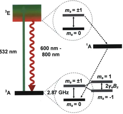
The negatively-charged nitrogen-vacancy (NV) center in diamond consists of a nitrogen atom and a vacancy that substitute two adjacent carbon atoms in the diamond lattice as shown in Fig. 2-1. For a single crystalline diamond, NV centers have four possible orientations as shown in Fig. 2-1. The four orientations lay along the tetrahedral axes of the host diamond. Figure 2-2 also illustrates the NV energy level diagram.
A spin magnetic triplet is formed at the ground state (3A), consisting of a sub-level
ms= 0 at its lowest energy and another two degenerate sub-levels mS = ±1 raised by -2.87 GHz, which is temperature dependant. Under green light (A~~532 nm)
excitation, the NV center spins are stimulated to their excitation states (3E in Fig. 2-2)
and then relax back to the ground state (3A). This is accompanied by spin dependant
red fluorescence, which is a unique proerty for NV centers. The relaxation of the m, = 0 state is accompanied with a bright red fluorescence (A~600~800 nm). In
Bz,~~~ ...---.... Bs
BeB 2
NV Orientation I
Figure 2-1: Nitrogen-vacancy centers in a diamond lattice. The blue, and red circles represent carbon, and nitrogen atoms respectively. The white circles represent the vacancy. The projections (B_1, B_2, B23, B 4) of an external magnetic field Bet along
the four nitrogen-vacancy axes are also shown.
04
600 nm
800 nm
S= It +1MS P too14 11 2yeU .7 G~z 'It% J M 114% MS= I I DI I % I 'S S.Sm,=± 1~
m=
0 S'Figure 2-2: The energy-level diagram of a nitrogen-vacancy center in diamond.
532 nm
non-radiative intersystem crossing into a metastable spin-singlet state ('A in Fig. 2-2), and then transition into the m, = 0 ground level reducing the red fluorescence
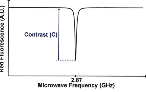
intensity. Therefore, by applying a microwave (fo = -2.87 GHz) and measuring the red fluorescence intensity of the NV center under green light excitation, the magnetic resonance of the NV can be detected (shown in Fig. 2-3). Since this resonance is detected optically, this is called optical detected magnetic resonance (ODMR) [6, 12]. As shown in Fig. 2-3, the amplitude of the dip at 2.87 GHz is called the contrast.
C
Contrast (C)
0
2.87
Microwave Frequency (GHz)
Figure 2-3: The red fluorescence intensity of the NV centers at varying microwave frequency (ODMR) under no external magnetic field bias.
2.2
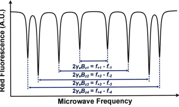
DC Magnetic Field Measurements Using NV
The two unpaired electrons in each NV center form anti-parallel spins in m, = 0 and
parallel spins in m, = i1. When an external magnetic field Bext with a component
B, along the N-V axis (see Fig. 2-1) is applied, the m, = ±1 sub-levels are split apart
higher energy than that of the m, = -1 level, where the two spins are parallel with
Bz, The photon frequency Af associated with such an energy gap is proportional to |Bz|:
Af =
f+
- f- = 2-/e|Bz|, (2.1)where -ye is the gyromagnetic ratio and equals to 28 GHz/T, and
f+
andf_
are the frequencies for the transitions from m, = 0 to m, = +1 and m, = -1, respectively.NV magnetometry is performed by determining
f+
andf-
via ODMR. We useAf to derive Bz. Through detecting the magnetic resonance using ODMR, a static or slowly-varying magnetic fields Bz, can be determined by sweeping a microwave frequency fo around 2.87 GHz and monitoring the average intensity. The observed resonances of Fig. 2-4 are
f+
andf-,
which give B,. Since NV centers have four possible orientations in a single crystalline diamond as discussed in Section 2.1, this leads to fourD (U) 0 2yeBzl f.1 - -.1 0 8 LL 2yeBz2
=f+2
- f-2 2YeBz=
f+3 - f-3 2yeBz4 = f+4 - f-4Microwave Frequency
Figure 2-4: The red fluorescence intensity of the NV center at varying microwave frequency (ODMR) under an external magnetic field bias with projections along the four N-V axes.
pairs of splitting in a single ODMR measurement (Fig. 2-4). The magnetometer based on this principle, therefore, has vector-field measurement capability by monitoring the different magnetic field projects and reconstructing Bez,. That is advantageous over conventional Hall and fluxgate-based sensors [13, 14], where three devices in x- y-
z-axes are needed for vector detection.
An NV-center vector magnetometer normally has a static bias field to create the aforementioned four ODMR spectral splittings (Fig. 2-4). The electronics of the magnetometer then tracks the shifts of
f+
andf_,
so as to measure the variation of the externally applied magnetic field. This can be done by recording the additional change of the sensor output red fluorescence intensity measurements around each dip in the magnetic resonance curve. Note this intensity change is caused by the shift of each resonance frequency Afi due to the projection of the added field on the associated NV-center axis ABzi (to be measured) on top of the bias static field. The sensitivity obtained from an ODMR spectrum as shown in Fig. 2-4 is determined by two factors: the linewidth and the signal-to-noise ratio (SNR) of each transition curve. The SNR is proportional to the contrast of the experiment and inversely propositional to the minimum detectable intensity signal. In Chapter 4, more details and an analytical expressions of the sensitivity are provided.Chapter 3
Chip-scale CMOS-Diamond
Magnetometer
3.1
CMOS-Diamond Hybrid Sensing Architecture
In the proposed CMOS-diamond sensing architecture, we use standard CMOS tech-nology to implement most of the components required to manipulate and readout the spin states of NV centers in diamond. A diamond layer full of NV centers is attached on the top of the chip. A green laser source is used for optical excitation. As shown in Fig. 3-1, a microwave signal generator, switches and current drivers that feed a microwave coupling structure are needed to manipulate the spin state of the
NV centers. The microwave signal generator has to operate over a sufficient range (i.e. 2.6 GHz to 3.2 GHz) to enable the measurements of the ODMR curve. The microwave
delivery structure which can be an inductor has to generate a strong homogeneous microwave field to increase the contrast of the ODMR curve (i.e. signal) and drive all the NV centers in the ensemble with the same strength.
In order to detect the spin dependant red fluorescence a photodiode on the chip is integrated below the microwave delivery structure. However, the absorption probability
of the NV to green light is very low, which means the majority of the green light transmits into the on-chip photodiode. This hurts the overall noise of the experiment, hence the sensitivity. This is due to two factors: (i) the intensity fluctuation of the green light. (ii) the shot noise due to the large output DC current which can be given
by Eq. 3.1:
i2 = 2qID/f - 2q(Ig + Ir)Af. (3.1)
where, Af is the noise bandwidth, and ID is the DC current detected by the photodiode. I., and I, are the green and red current portions detected by the photodiodes. This green background also hurts the contrast of the ODMR curve, which consequently hurts the sensitivity. Therefore an optical filter is needed to suppress the green excitation light and pass the red fluorescence. This filter should be added between the diamond and the photodiode. We choose to integrate this filter on the same chip; pushing towards a monolithic solution using standard CMOS process.
3.2
CMOS-Diamond Hybrid Quantum
Magnetome-ter
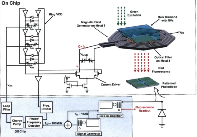
Figure 3-2 shows the system schematic of the first prototype of the hybrid CMOS-diamond quantum magnetometer. This chip, using TSMC 65 nm CMOS technology, integrates most of the critical components for the ODMR operation. Shown in Fig. 3-2, an on-chip ~ 2.87 GHz voltage-controlled oscillator (VCO) is phase-locked to an external reference with a tunable frequency. Through a differential current driver and a loop inductor, the circuit applies a vertical AC magnetic field to excite the m = 1 ground levels of NV centers inside a thin layer of nanodiamond particles.
Filter+ ...- Green
:Green
Microwave Coupling Photodiode ..- ' ..--- i :Excitation. Structure ..---.
---Diamond
-*with NVs
MicrowaveSignal DMicrowave
Generation Coupling Structure
Optical Filter
... ... P od o e
~~Ph odiode
Readout ''s
Circuit
'-Figure 3-1: The basic schematic of the proposed CMOS-Diamond sensing architecture.
On Chip
Ring VCO Green U 1 0 ' Nano Diamond Excitation L with Ns
Magnetic Field Generator on Metal 9
cuus
Swich 5 Opt Cal Filter
Son Metal 8
Ih 0
5506
gags, 0 Red Y V~VV Fluorescence
Vem Current Driver Patterned
Photodiode fm-1KHz
Loop Freq. |Oz!
Filter Divider Fluorescence
Readout
Lock-in amplifier | Phase/
Charge - -uonc
Pump Frqenyfo0Mr Detcto - i-0MN
Off Chip
Si nal Generator
Figure 3-2: The schematic of the first CMOS-diamond quantum magnetometer with a layer of nanodiamond on the top of the chip.
The nanodiamond coating is formed by appling the nanodiamond solution on the chip surface and then evaporated the liquid (extra details are given in Section 3.6.1). The nanodiamond is excited from above with a green light, and the red fluorescence is detected by a p+/n-well/p-sub photodiode placed under the loop inductor. The
On Chip
is @~ Green
Ring VCO Excitation Bulk Diamond Magnetic Field I with NVs Generator on Meta 9 Ctd VDD 3 3 S 3 U Optical Filter VI IV4*I on Metal 8 egging Red Fluorescence
V rrent Driver PhotodlodePatterned
...
LoopFreq Ogg Fluorescence
Filter Divider Readout
f% - 1 KHz oki mlfe Chre Phase/
aFrequency fa-10MzO
Off Chip
I Signal Generator|
Figure 3-3: The schematic of the first CMOS-diamond quantum magnetometer with a single crystalline slab on the top of the chip.
diode is partitioned into smaller portions in shunt, in order to prevent the induction of large eddy current from the inductor (hence RF loss). As described in Section 3.1 the majority of the green light is not absorbed by the diamond, but transmits into the chip. A plasmonic nano-photonic filter, using a grating of the CMOS interconnect metal (Metal 8), is implemented above the photodiode (Fig. 3-2). The detailed design of the filter is provided in Section 3.4. In addition, techniques for improving the overall filtering performance are discussed in Chapter 5.
The lattice orientations in the nanodiamond particles are random. This means the amount of frequency splitting in each NV is also random. As a result, the resulting ODMR can be only used for scalar-field sensing. Another prototype with a slab of single crystalline diamond attached to the same CMOS chip as shown in Fig. 3-3 is also reported. This allows for vector-field sensing capabilities. The diamond is also cut
and attached in a way that direct the green light horizontally to enhance the filtering as explained in Section 3.6.2.
3.3
On-chip Microwave generation
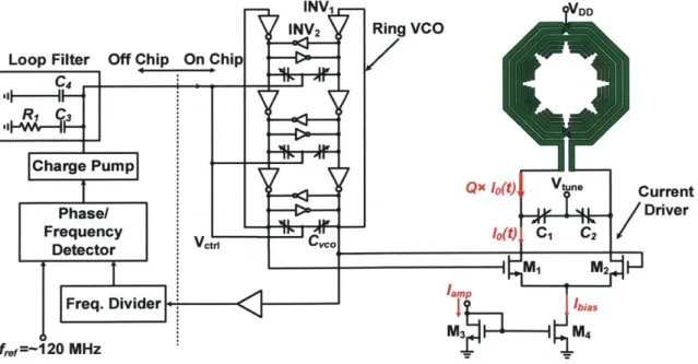
The ground-state spin transitions are driven by the on-chip generated microwave fields. Figure 3-4 shows the circuitry for on-chip microwave generation and delivery. This circuitry is composed of a phase-locked loop (PLL), a current driver, and a resonant loop inductor. The PLL generates the microwave sweep signal from 2.6 GHz to
3.1 GHz required for the ODMR experiment. The main component of this loop is an
on-chip voltage-controlled ring oscillator (VCO) with 3 differential inverter stages. The usage of a ring VCO [15] avoids any large-size inductor and minimizes the cross-talk between the oscillator and the microwave inductor which drives the NV ensemble. The mutual-locking inverter pair (e.g., INV2 in Fig. 3-4 forms a latch and ensures the differential phases between the left and right branches of the VCO. Inside each inverter stage of the on-chip ring VCO in Fig. 3-4 (e.g., INV1), the sizes of the NMOS and
INV1, INV2
Loop Filter Off Chip On Chip
C4 Charge Pump-Phasel Frequency V Detector er c [Freq. Divider f,o«=~120 MHz Ring VCO VoD
Qx lo(t) Vtune Current
/
Driver lo(t) C1 C2 SM1 M2 lamp 'bias M 3 M4PMOS (gate width/gate length) are 24 pm/280 nm and 54 pm/280 nm, respectively. Inside each latch inverter (e.g., INV2 in Fig. 3-4), the NMOS and PMOS sizes are
5.2 pm/280 nm and 12 pm/280 nm, respectively. The frequency tunability of the
oscillator is realized via 3 pairs of MOS variable capacitors (e.g., Cvco in Fig. 3-4, of which the capacitance changes from 22 fF to 75 fF when the PLL control voltage
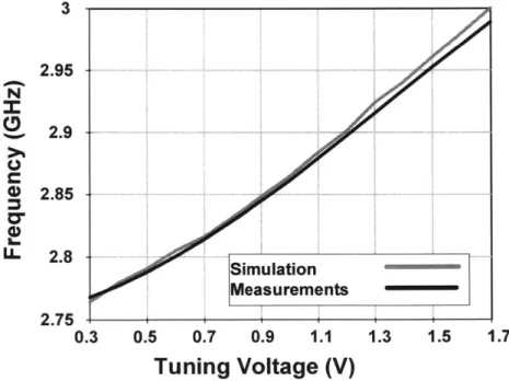
Vtri varies from 0 to 5 V. The simulated and the measured VCO tuning curves are
shown in Fig. 3-5. The curves show very good agreement between them. The VCO gain is ~180 MHz/V. The entire phase-locked loop is closed with off-chip components to enhance the stability and decrease the phase noise of the signal. The loop filter of the PLL is a typical second-order low-pass filter and the values of the components shown in Fig. 3-4 are R1=0.4 kQ, C3=4.5 nF and C4 =150 pF.
The microwave fields are delivered to the NV ensemble through the loop inductor (Fig. 3-4) implemented on the top-most copper layer (Metal 9). To efficiently deliver the microwave field, the loop inductor and a pair of shunt capacitors (C1 and C2 in Fig. 3-4) form a resonating load for the current driver. C1 and C2 are MOS variable
3 2.95-N 2.9 0 2.85 L.. LL 2.8 2.75 0.3 Simulation Measurements 0.5 0.7 0.9 1.1 1.3 1.5 1.7
Tuning Voltage (V)
capacitors with capacitance ranging from 312 fF to 1.4 pF. By electrically tuning them via Vtue, the load resonates near Dgs as shown on Fig. 3-6. This current driver fed by the output of the ring VCO produces oscillating current in the inductor at the VCO microwave frequency. In Fig. 3-4, the sizes (gate width/gate length) of transistors M1~M4 are 80 im/280 nm, 80 pm/280 nm, 72 pm/500 nm and 720 pm/500 nm, respectively. To improve the performance of this inductor for advanced NV sensing protocols [16, 17], we need to increase the applied microwave field amplitude. The amplitude is enhanced by a factor
Q
compared to the driver DC bias current (Ibias~ 5 mA from a 2.5 V power supply), where
Q
(~ 15) is the quality factor of theinductor. In addition, a three-turn loop is used to multiply the microwave field strength. Overall, we have 25x enhanced microwave field strength compared to a non-resonant single turn loop. The High-frequency electromagnetic fields simulations
(HFSS) result is plotted in Fig. 3-7. The magnetic field amplitude is plotted as a
function of distance from the inductor center
The advanced NV sensing protocols mentioned above also require highly uniform microwave fields over the excitation volume. To achieve this, three capacitive parasitic loops are inserted. The radius of the these loops is tailored, so that their opposite induced field homogenize the overall generated field. Another degree of freedom is the capacitive gaps in the parasitic loops. This controls the amount of current flowing in these loops. A comparison between the field distribution of a simple one turn loop and another one with the capacitively loaded parasitic loop as a function of the distance from the center of the inductor is shown in Fig. 3-8. This loading enhances the homogeneity of the field without sacrificing the field magnitude. The two important parameters (i.e., the parasitic loop radius and the capacitive gap) for the three parasitic loops are optimized to achieve > 95% uniformity. The detailed dimensions of the final loop inductor implemented in the chip is shown in Fig. 3-9. The loop outer diameter is 236 pm, and exhibits an inductance of -3 nH.
1.8 2 2.2 2.4 2.6 2.8 3 3.2 3.4 3.6 3.8
Frequency (GHz)
Figure 3-6: The amplitude of the AC current flowing in the inductor as a function of frequency. The plot shows a resonance behavior at 2.87GHz.
1 4
E
CD C3 CM Res. 3-turn -on-res. 1-turn 25X 1.4 1.2-N 0.8- 0.6- 0.4- 0.2--45 -30 -15 0 15Distance from antenna center (pm)
Figure 3-7: The simulated magnetic field profiles as a function of distance from the center of the proposed resonant inductor and a non-resonant one.
14-12 -U.. =O 0 LL
aO
10-8
6 4 20
K
30 451.4 1.2
E
%N, ca1=
0.8- 0.6- 0.4- 0.2-T I V 0-R 1-R/4
0
R/4
R/2Distance from inductor center
Figure 3-8: The simulated magnetic field profiles as a function of distance from the inductor center with and without capacitive parasitic loop.
l0p Metal 9 Via 8-9 Metal 8 Via 7-9 11 8p Spi -Metal 7 236p
Figure 3-9: The layout of the 3-turn on-chip inductor with parasitic capacitive loops.
9 4 ----- ---4% ... f. ... I
--S
2.6p -H3.4
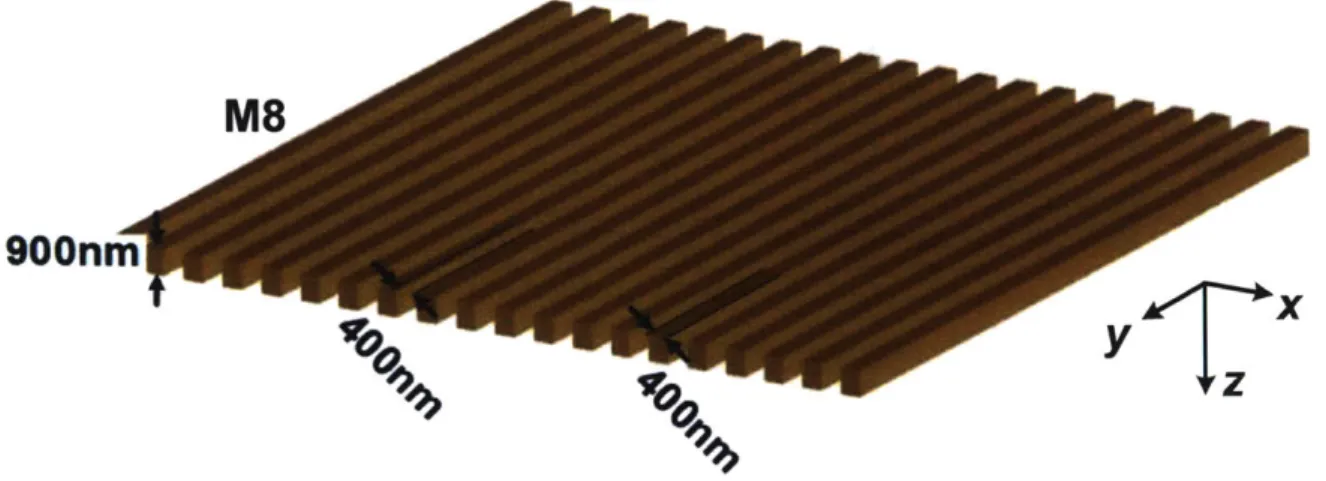
On-chip Optical Detection
The NV spin transitions are detected using an on-chip photodetector. A CMOS-compatible periodic metal-dielectric structure in the Metal 8 interconnect layer filters green pump light (Fig. 3-10). The incident light couples to the surface plasmon polariton (SPP) at the metal-dielectric interface, where it undergo frequency-dependent Ohmic loss [18, 19]. Therefore green light is attenuated more than red light, achieving a finite green to red rejection. As shown in Fig. 3-10 each slit is considered as a parallel plate waveguide transmitting light inside a dielectric (relative permitivity ed) in the z-direction. The incoming light is modeled as a plane wave with a transverse electrical field E., and a propagation constant ko=owVQ/c (c is the speed of light in vacuum). Then, it is coupled to the TEM mode of the parallel-plate waveguides, which has identical propagation constant ko. As the propagating wave interacts with the metal, the surface plasmon polariton (SPP) mode at the metal-dielectric interface is excited. Note that the dispersion relation of SPP mode is:
kzSPP =OSPP + jcespp = ko E (3.2)
Em + Ed
900nm
Figure 3-10: The layout of the single-layer plasmonic grating filter impleniented on Metal 8.
0 0 c,-10 0 .wI w 4--j -15- A > OC ~E -20- A 2-0 -25--30- 0 , 500 600 700 800 500 600 700 800 Wavelength (nm) Wavelength (nm) (a) (b)
Figure 3-11: The (a) real and (b) imaginary parts of the relative dielectric constant of copper. The calculated plots (solid lines) are based on the Drude-Brendel-Bormann model. The measured data (triangles and squares) are from 120, 21].
To quantify the loss of the SPP mode using the real and imaginary parts of the dielectric constant of copper shown in Fig. 3-11, the attenuation factor aspp is derived in (3.2):
caSPP = Im(ko + ~ k0 emi (3.3)
where em=Emr + jcmi is the permittivity of the metal, which is copper for M8 in
the technology we use. This exhibits large difference between red (aSpp~O.O1ko)
and green (asppe0.26ko). That is due to not only the decreased Emr of copper in green, which is normal plasmonic property described by the Drude model, but also an abnormal dispersion with increased emi, which is caused by interband transitions of bound electrons excited by the photons. The relative permitivity of the dielectric (Ed)
is 1.5 in the above calculations.
The simulated Lumerical FDTD transmission through the filter at the wavelengths of 532 nm (green) and 700 nm (red) are shown in Fig. 3-12. The measured green-to-red
0.5
0.5
(a) (b)
Figure 3-12: FDTD simulated light transmission through the optical filter at (a) green light (A=532 nm) (b) red light (A=700 nm).
suppression ratio due to this filter (d=900 nm) is 10 dB. Increasing the slit thickness
by stacking more grating layers (in M7, M6...) is expected to further increase the
suppression of the green light [19]. However, that causes degradation of red-light transmission due to the scattering at the side walls formed by the sparse inter-layer via pillars.
To detect the NV-emitted red fluorescence, a P+/N-well/P-sub photodiode as shown in Fig. 3-13a is used. This specific configuration is preferable for long wavelength detection [22]. Since we place the photodiode with its conductive layers below the inductor (Fig. 3-2), large eddy currents near 2.87 GHz can be induced if we use a conventional unpatterned physical layout as shown in Fig. 3-13b. This reduces the quality factor of the inductor, resulting in microwave amplitude reduction. By dividing the photodiode area into four subareas (2x2 array) as shown in Fig. 3-14a, this eddy current is reduced by half as shown in Eq. 3.4, and Eq. 3.5:
Peddy X (d@(t)/dt)2 L4 ( )2 (3) dB 234
R L o dt
PeddyProp 3( =(.)
3 5)
PeddyConv La 2
Cathode P+ Layer
Anode N-Well Cathode
Connection N-Well EddyL Currents Anode P Substrate Connection ___________________________________P Substrate (a) (b)
Figure 3-13: (a) The cross section of the P+/N-well/P-sub (b) unpatterned photodiode layout with eddy current loops in the active area and possibly the anode and cathode connection.
and B are the magnetic flux and the magnetic field generated by the loop inductor in Metal 9, respectively. t is the time and R is the active area resistance. Similarly,
by dividing the photodiode active area into N x N subareas, the eddy current loss is
reduced by 1/N. Furthermore, the anode/cathode connectors are arranged in a radial way that is similar way to patterned ground shielding used in CMOS inductors [23]. This arrangement (Shown in Fig. 3-14b, and Fig. 3-14c) avoids any closed loops, which helps to cut the eddy current that may flow in the metallic connections. As shown in Fig. 3-14d the eddy current loops flow only in the patterned active area only. The photodiode has a measured responsivity of 0.23 A/W at the wavelength of
532 nm, which corresponds to a quantum efficiency of 0.54.
3.5
Passivation Layer Etching
The chip is fabricated with a standard 65nm low-power CMOS technology from TSMC. This CMOS technology provides a top nitride layer for surface passivation. This passivation layer emits unwanted background red fluorescence under green excitation. Fig. 3-15 shows an optical image for the red fluorescence of the chip with and without
P+ Layer N-Well L Shallow-Tnch Isolation (STI) (a)
N-Well P+ Layer Cathode Connection Anode Connection Shallow-Trench Isolation (STI) (c) P+ Layer N-Well Anode Connection Shallow-Trench Isolation (STI) (b)
N-Weil P+ Layer Cathode Connection Anode Connection Eddy Currents Shallow-Trench Isolation (STI) (d)
Figure 3-14: The proposed patterned photodiode layout (a) 2x2 active area layout (b) the radially connected anode connection that prevents any closed loops implemented in M1. (c) the full layout with cathode connection in M2 added. (d) the full layout with eddy current loops in the patterned active area only.
passivation etching. As the figure clearly shows fluorescence intensity drops significantly after the passivation removal. CF4 plasma dry reactive ion etching is used in this process. The etching is done at the clean rooms at MIT. This is the only post processing step required after fabrication. However, this step can be done later at the CMOS foundry for product level fabrication in the future. In the measurements discussed in this thesis, we focus on ensemble measurements (more details in Chapter 4) . The background noise that may come from the passivation layer doesn't affect much the SNR of the experiments discussed in this thesis. However, In future experiments, where we address single or small number of NV centers (Chapter 5), this background
15000 E 15000 50 50 'A n 100 10000 100 10000 150 150 5000 5000 4. 200 200 250 250 50 100 150 200 250 50 100 150 200 250 (a) (b)
Figure 3-15: Optical image for the red fluorescence emitted by the chip surface under green excitation (a) without passivation layer removed (b) with passivation layer removed. Scale bar is 100pm.
noise can be very critical.
3.6
Diamond Sample Preparation
As mentioned in Section 3.2, two prototypes in this thesis are discussed. The NV centers is embedded in nanodiamond layer that covers the chip in the first one, and in a slab of single crystalline diamond in the second one. The diamond sample in both cases are placed on the top of the chip on the sensing area (See Fig. 3-16a) including the on-chip inductor, the optical filter and the photodiode. In this section, the preparation of both samples and how they are deposited on the top of the chip are discussed.
3.6.1
Nanodiamond Placement
A solution of nanodiamond particle is deposited on top of the chip by adding a droplet
using pipette. The solution then evaporates leaving the nanodiamond particles on the chip surface after drying. Figure 3-16b shows the sensing area of the chip with the nanodiamond particle covering the chip.
3.6.2
Bulk Diamond Placement
A 500 pm x 500 pm x 500 pm diamond slab is picked and placed on top of the chip
under a microscope. The diamond is a single crystalline CVD-grown diamond from
Element 6. It is electronically irradiated with a dosage of 1018 e- /cm2 at 1 MeV, and then annealed for 2 hours at 8500C. This produces an estimated NV centers density
of - 0.01 ppm. Immersion oil is used to adhere the diamond slab to the chip. By
bridging the difference of the refractive index, the oil also minimizes the fluorescence loss. A 450 cut is introduced in the diamond's corner as shown in Fig. 3-3 to direct the vertical incident green laser horizontally to further enhance the overall green rejection ratio. Fig. 3-16c shows an optical image of the diamond slab on top of the chip.
On-chip
Inductor
*N
Sensing Area
(Optical Filter &
Photodiode)
(a)
Nanodiamoid Particles
Single
Cry al
Diamond
(b) (c)
Figure 3-16: Top-view micrograph of (a) the fabricated CMOS chip sensing area including the inductor, optical filter, and photodiode. (b) the same area on the chip covered with nanodimaond particles. (c) the sensing area covered by the single crystalline diamond slab. Scale bar is 100pm.
Chapter 4
Experimental Results
In this section the measurement results of the two prototypes discussed in Chapter 3 are introduced. The CMOS chip is wire-bonded on a PCB board. The PCB photo with the chip micrograph are shown in Fig. 4-1.
4.1
Nanodiamonds Results
We start with measuring the ODMR of the nanodiamonds attached on top of the chip using external optical detection. This step is important to verify the operation of the microwave source. Figure 4-2a shows the test setup of the experiment. A linearly polarized DPSS green laser beam (2 W, A = 532 nm, Verdi G2, Coherent) is delivered
to the diamond through a telescope of fi = 35 mm and f2 = 150 mm. The beam
diameter incident on the diamond is -500 pm. The lens system given is used as our laser is placed far from the sample for experimental convenience, though it is important to note that the lens system could be avoided if the laser was positioned nearby the CMOS chip or even replaced with other options as discussed in Chapter 5. The microwave frequency is swept to address the NV center and excite the magnetic resonance. This is done by changing the reference frequency of the PLL loop through external signal generator (~ 120 MHz). The VCO output signal is frequency-divided
Microwave
0.8mm
Generation Circuitry
0s
3"
Sensing Area
Figure 4-1: Optical micrograph of the CMOS chip (bottom) and photo of the printed circuit board for testing (top).
A
EM-CCD 0 0-, Bext, = 0 .-S0.98Bex = 1.72 mT--%4 0.96 0.96-Dichroic U) 532 nm 0.94 Laser Microscope 0.92 Objective E 0.9-Diamond 0 LayersZ 0.88. 2.8 2.82 2.84 2.86 2.88 2.9 2.92 2.94 . Frequency (GHz) (a) (b)
Figure 4-2: (a) The experimental setup of the ODMR experiment using off-chip camera.
(b) The corresponding measured and fitted ODMR spectrum at no external magnetic
field and at 1.72 mT permanent magnet.
by 24 and then compared to the refrence signal provided by an external signal source
(HP ESG-D4000A). Then the spin dependant red fluorescence is collected using a camera. As shown in Fig. 4-2b, an ODMR spectrum is measured under no external biasing magnetic field. Due to the strong microwave signal genertated by the chip a contrast of 10% is successfully obtained. An external magnetic field through a permanent magnet is then applied. Figure 4-2b shows an extra broadening in the ODMR curve in this case, which corresponds to the Zeeman splitting of the randomly oriented NV centers. Spectral broadening, rather than splitting, is observed because the effective Bz (hence the amount of splitting) for each orientation varies. The magnetic field of the permanent magnet is estimated through curve fitting to be
1.72 mT.
The next step is to test the whole on-chip system by detecting the NV red fluorescence using the on-chip photodiode. Similar laser setup is used as the one shown in Fig. 4-2a, However, lock-in amplifier is used to detect the photodiode signal as shown in Fig. 3-2, and Fig. 3-3. In this experiment A half-wave plate rotates the
14 i 12- Bext2
=2.2
mT
-C 8-r 6-2. 0 2.8 2.82 2.84 2.86 2.88 2.9 2.92 2.934Frequency (GHz)
Figure 4-3: The measured and fitted ODMR spectrum using on-chip photodiode at
no external magnetic field and at 2.2 mT permanent magnet.
polarization of the laser beam to maximize the laser absorption through the periodic
mietal/dielectric structure in the Metal 8 layer. Since the filter rejection is still only
10 dB, there is a huge background green signal that complicates the measurements. A lock-in detection technique is used to detect the NV red fluorescence. The green
laser beam continuously excites the NV ensemble, and the amplitude-modulated
(AM) microwave fields (fm = 1 kHz) drive the NV electron spin transition. This is done by switching the microwave signal on and off with
fm,
rate (Fig. 3-2). The spin-dependent fluorescence produces photo-current within the on-chip photodiode. Then, the modulated photo-current is detected through the voltage drop across a 50 Q resistor atfm,
with a Stanford Research Systems lock-in amplifier (SR865A). The use of the lock-in amplifier rejects the DC current offset of the photodiode, which is causedby the unmodulated green laser, and avoids the low-frequency flicker noise accordingly.
The measured ODMR is shown in Fig. 4-3. Similar to the off-chip detection experiment,
-The ODMR with and without external magnetic field is recorded. A clear Zeeman splitting is observed when 2.2 mT from permanent magnet is applied. Replacement of nanodiamond with single-crystalline diamond addresses spectral broadening issue, which is due to the random orientation of NV centers, and helps in demonstrating vector field sensing as discussed in Section 4.2. In this experiment the sensitivity of the sensor is estimated as given in Eq. 4.1:
S = - v t. (4.1)
7e C
Here, u is the noise over the measured data, Av is the linewidth of the ODMR curve in Fig. 4-3. -ye is the gyromagnetic ratio (28 GHz/T), C is the contrast, and t is the integration time. The calculated DC magnetic field sensitivity of 74 pT/v Hz.
4.2
bulk diamond Results
To detect the ODMR of an ensemble of NV centers in a single crystalline diamond slab, a similar setup as discussed in Section 4.1 is used, in addition to the same laser setup as before, but with laser power of 500 mW . Although the overall filtering for the green light is enhanced due to the cut introduced in the diamond, there is still huge green light background detected by the photodiode. A lock-in technique is also used in this experiment. The green laser beam continuously excites the NV ensemble, and the frequency-modulated (FM) microwave fields (fm = 1.5 kHz and modulation
depth of 6 MHz) drive the NV electron spin transition (Fig. 3-3). A 50 Q resistor is also used here to read the photocurrent at
fm
with one second integration time, which corresponds to the equivalent noise bandwidth of 0.078 Hz (considering the filter roll-off of 24 dB/oct) of the lock-in amplifier.Figure 4-4 shows the lock-in signal for the ODMR experiment under zero external magnetic field applied. This spectrum corresponds to the derivative of the ODMR
I I I I I I I I
>
600
*
400
C
200
S01
-200
--o
-400-
-600-2.7
2.75
2.8
2.85
2.9
2.95
3
3.05
Frequency (GHz)
Figure 4-4: Frequency-modulated (FM) lock-in signal of NV spin-dependent fluores-cence at zero external magnetic field.
spectrum shown in Fig. 2-4. Next, a permanent magnet (6.27 mT) is aligned to split the spin transitions of the four NV orientations. Figure 4-5 plots the ODMR spectrum, which exhibits the expected eight spin transitions (Fig. 2-4). The use of the corresponding four NV ensembles enables vector magnetometry. In particular, it is
important to note that the spin transitions at v_ = 2.8303 GHz and v+ = 2.9330 GHz
of the NV ensemble.
Monitoring the lock-in signal V at v_. and v+ enables independent measurements of magnetic field and temperature. Specifically, the sum of the lock-in signal change AV at vi± is proportional to AT, while the difference provides ABz:
11 AV AXV A T = 1 V + AV(4.2) 20T dV/df + dVdf (4_ and
1
(Av
AV
ABZ = .VA (4.3) 2-ye dV/df + dVdfv) (150-C
100-e
5 0-
-50---100
-150
2.7
2.75
2.8
2.85
2.9
2.95
3
3.05
Frequency (GHz)
Figure 4-5: FM lock-in signal with a permanent magnet (B = 6.27 mT). The linewidth
of the ODMR is 7 MHz. Slopes dV/df at v- = 2.8303 GHz and v+ = 2.9330 GHz are
42.969 nV/MHz and 42.450 nV/MHz, respectively.
center frequency shift (red). The square-wave magnetic field applied in Fig. 4-6 is generated by an electromagnet. Alternating electrical current is used to avoid magnetization. lock-in signals at both v± are observed while switching the polarity of external electromagnet with a period of 26 min. The center frequency shift represents the temperature shift in the experiment which is calibrated to determine the magnetic sensitivity. The magnetic field sensitivity is given by the following relation:
S = UB, (4.4)
VENBW
Here, B,B is the noise in AB, measurement, and ENBW is the equivalent noise
bandwidth of the lock-in detector. In the measurements, ENBW = 5/(64T) with a
time constant T of 1 second, accounting for the 24 dB/oct of the lock-in amplifier filter roll-off. By measuring UB, of 6.3 [pT from the modulated spin-dependent fluorescence (Inset in Fig. 4-6), a DC magnetic field sensitivity of 32.1 pT/Vii is determined. The
2053
5
25tL " -d f ---SU --. 32 -250-50
0
20
40
60
80
100
120
Time (min)
Figure 4-6: On-chip magnetometry (Blue) and temperature effect (Red) separation by detecting the effect of switching electromagnet on v± of the ODMR curve of Fig. 4-5.
sensitivity includes additional V/2 factor of v+ and v- signal average. This DC magnetic field sensitivity is limited by the noise detected in the ENBW at
f
m = 1.5 kHz.In order to understand the contribution of each component on the overall noise performance of the system, the noise is measured using the lock-in amplifier. The measured overall noise in the experiment is 38 nV/v/III at
f
m = 1.5 kHz. This isprimarily because of from the green laser intensity noise, due to the limited performance of the optical filters. This laser intensity noise is orders of magnitude larger than other noise sources:
1. The thermal noise of the 50 Q resistance (R), which is used to convert the
photo-current to voltage. This noise is 0.9 nV/vlz¶ as calculated from Eq. 4.5:
V2=
4KTRAf. (4.5) where K is the boltzman constant, T is the temperature, and A f is the band-width.2. The NV red fluorescence shot noise is - 9 pV/vHz at fm 1.5 kHz as given in
Eq. 4.6:
V-2= R2(2qiD)Af ~ R2(2q
DaAf.
CR (4.6) where Vmax is the maximum voltage in the ODMR curve in Fig. 4-5, which is
100 nV, C is the ODMR contrast - 0.02, and q is the electronic charge.
3. The amplitude noise converted from the microwave generator spectral purity
is 1 fV/V Hz (see Eq. 4.7). The measured phase noise (#p) of the PLL is -90 dBc/Hz at an offset frequency of 1.5 kHz (FM modulation frequency fmn).
V2
c (Vq5fm/) 2Af. (4.7)where V, is the signal voltage amplitude, and
#
is the slope of the FM-ODMR curve. We assume that p < 1.Chapter 5
Conclusion and Future Work
In this thesis, the first implementation for a chip-scale quantum magnetometer by integrating diamonds with CMOS technology is reported. An architecture in which the essential components to detect NV-ODMR - a microwave generator, an inductor, an optical pump beam filter, and a photodetector - are fabricated throughout the
CMOS multi-layers is created. Two prototypes to address NV spin ensembles in a layer
of nanodiamond particles and single crystalline diamond slab. In the nanodiamond prototype, the measured sensitivity is 74 pT/v/Hz for scalar field magnetic field sensing. In the second experiment with single crystal diamond, vector-field magnetic field measurements are realized. The sensor magnetic sensitivity is 32.1 pT//l Hz.
In the prototypes reported in this thesis, the achieved magnetic field sensitivity is orders of magnitude worse compared to the best DC sensitivities reported: 290 pT/v/fzl and 28 pT/v/III for vector [101 and scalar [11] magnetometry, respectively, to our best knowledge. The sensitivity is mainly limited by the green laser intensity noise as described in Chapter 4. However, this performance can be improved by including (i) metal gratings in multiple CMOS metal layers based on the wavelength-dependent Talbot effect [24] and (ii) fabricating a resonant grating [25] in diamond. These additionally attenuate the green laser and consequently reduce the laser intensity noise
by several orders of magnitude. In addition, using a diamond waveguide geometry [10],
possibly with a higher NV density [26] (0.01 ppm to 10 ppm), should increase the signal-to-noise ratio (SNR) by orders of magnitudes. Moreover, dynamical decoupling sequences [16, 17, 27] can improve the sensitivity by a few orders of magnitude for
measuring magnetic fields at frequencies above the NV decoherence rate.
For practical sensor realization in the future, one critical component not presently integrated into the presented CMOS-diamond platform which is the pump laser for
NV optical excitation. This optical pump can be integrated into the platform through
using a chip-scale laser diode [28], green Vertical-Cavity Surface-Emitting Lasers [29], or CMOS-compatible waveguided delivery of the optical pump beam [30]. It is also important to note that the CMOS-integration of all currently off-chip electronic components, such as the phase-locked loop with frequency modulation and the lock-in amplifier, has been demonstrated in prior research
[31].
These indicate the feasibility of millimeter-scale form factor for future quantum-sensing systems.This hybrid CMOS-diamond platform can be extended toward on-chip sensing of other quantities such as electric fields. The architecture can also be extended towards an imaging platform (see Fig. 5-1). An array of photodiodes can be implemented below the microwave delivery structure to create the image by measuring the NV-ODMR on each pixel. In addition to chip-scale quantum sensing capability, the CMOS-based spin control and readout scheme presented in this thesis can uniquely provide a scalable solution for implementing spin quantum-bit (Qubit) controls. This is, in particular, essential to develop a large-scale quantum system [1, 2, 32, 33]. A conceptual scheme is shown in Fig. 5-2. Individual on-chip control and readout of Qubits can be implemented. Since the required components are integrated in the same platform, feedback control can be implemented through on-chip logic. This would enable on-chip quantum information processing [34-36].
Microwave Delivery StructureI g Photodio A rray Microwave Signal Generation and Switching Electric Field .. T. Tuning ntroiu Ciogic
Figure 5-1: NV-based magnetic imager with an array photodiodes below a single microwave delivery structure.
Qubit Node ---... ..---.. Electric Field Tuning Microwave Control Readout Circuit Electric Field Tuning Microwave Control Readout Circuit
Microwave Delivery Photodiode Structure Qubit Electric Field Tuning Microwave Control I Readout Circuit Control logic
Figure 5-2: NV-based individual Qubit control for scalable quantum information processing applications.