HAL Id: hal-01633539
https://hal.archives-ouvertes.fr/hal-01633539
Submitted on 2 Feb 2018
HAL is a multi-disciplinary open access
archive for the deposit and dissemination of
sci-entific research documents, whether they are
pub-lished or not. The documents may come from
teaching and research institutions in France or
abroad, or from public or private research centers.
L’archive ouverte pluridisciplinaire HAL, est
destinée au dépôt et à la diffusion de documents
scientifiques de niveau recherche, publiés ou non,
émanant des établissements d’enseignement et de
recherche français ou étrangers, des laboratoires
publics ou privés.
Sensitive spin detection using an on-chip
SQUID-waveguide resonator
G. Yue, Lin Chen, J. Barreda, V. Bevara, L. Hu, L. Wu, Z. Wang, P. Andrei,
Sylvain Bertaina, I. Chiorescu
To cite this version:
G. Yue, Lin Chen, J. Barreda, V. Bevara, L. Hu, et al.. Sensitive spin detection using an on-chip
SQUID-waveguide resonator. Applied Physics Letters, American Institute of Physics, 2017, 111 (20),
pp.202601 - 202601. �10.1063/1.5006693�. �hal-01633539�
arXiv:1710.10506v1 [cond-mat.mes-hall] 28 Oct 2017
G. Yue,1, 2,a)L. Chen,3 J. Barreda,1 V. Bevara,4, 2 L. Hu,1 L. Wu,3 Z. Wang,3 P. Andrei,4, 2 S. Bertaina,5 and I. Chiorescu1, 2,b)1)Department of Physics, Florida State University, Tallahassee, Florida 32310,
USA
2)National High Magnetic Field Laboratory, Florida State University, Tallahassee, Florida 32310,
USA
3)CENSE, State Key Laboratory of Functional Material for Informatics, SIMIT, Chinese Academy of Sciences,
Shanghai 200050, China
4)Department of Electrical and Computer Engineering, FAMU-FSU College of Engineering, Tallahassee,
Florida 32310
5)Aix-Marseille Universit´e, CNRS, IM2NP (UMR 7334), Marseille, France
(Dated: 31 October 2017)
Precise detection of spin resonance is of paramount importance to achieve coherent spin control in quantum computing. We present a novel setup for spin resonance measurements, which uses a dc-SQUID flux detector coupled to an antenna from a coplanar waveguide. The SQUID and the waveguide are fabricated from 20 nm Nb thin film, allowing high magnetic field operation with the field applied parallel to the chip. We observe a resonance signal between the first and third excited states of Gd spins S = 7/2 in a CaWO4crystal, relevant
for state control in multi-level systems.
Solid state spin-based qubits are studied for quan-tum computing due to their relatively long coherence time1,2. Typical implementations of these qubits are
molecule-based magnets3–6, nitrogen-vacancy (NV)
cen-ters in diamond7 and quantum spins in crystals8–11.
These spin-based qubits are designed such that the spins are well separated in the crystal, leading to an increased decoherence time due to weak spin dipolar interactions.
Among the rare-earth ions, S-state lanthanide ions doped in a crystal have a rich energy level structure due to their large spin. Multi-level systems are promising for implementing few-qubits algorithms12or as quantum
memories13–16. For quantum technology applications, a
higher sensitivity electron spin resonance (ESR) measure-ment is needed to be able to manipulate spins in meso-scopic crystals placed on superconducting chips17–21.
Compared to other ultra-high sensitivity ESR measurements22,23, the use of Josephson junctions can
increase significantly the spatial resolution of the mag-netic detection while allowing an on-chip implementa-tion. For instance, the magnetic signal of one nanopar-ticle is detectable if placed on the junction of a microm-eter sized superconducting quantum interference device (micro-SQUID)24. We present a novel setup for ESR
measurements, which combines the high spin sensitiv-ity of an on-chip micro-SQUID and the flexibilsensitiv-ity of a coplanar waveguide for microwave excitation. Differ-ent dc-SQUID implemDiffer-entations were also used to detect molecular25,26 and diluted27 spins. In our case, the
cou-pling of the two devices generates a cavity effect, which amplifies the microwave power seen by the spins. When using micro-SQUIDs, the samples are positioned close to their loop for increased sensitivity since the device
a)Electronic mail: [email protected] b)Electronic mail: [email protected]
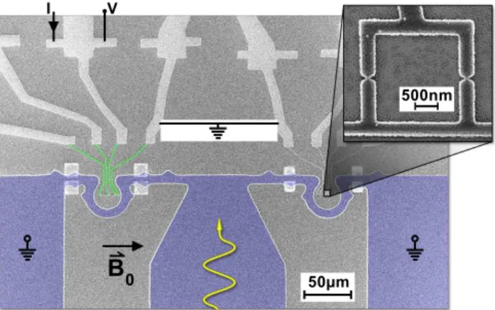
FIG. 1. (color online) Scanning electron micrograph of the device and of the micro-SQUID (inset). The darker (blue) area is the coplanar waveguide with the two Ω-loop shortcir-cuits between the central line and the lateral ground planes. The microwave excitation is depicted by the curvy arrow and an in-plane field ~B0 is generated by an external coil. The
SQUIDs share a common ground (sketched as a white rect-angle). Each SQUID has one I − V line shown in green for clarity in their narrowest region.
can work under in-plane magnetic fields in the range of ∼Tesla28–30.
Using this setup, we successfully measured the reso-nance signal of Gd3+ S = 7/2 ions diluted in a CaWO
4
single crystal with a concentration of 0.05%. Moreover, the resonance is between the first and third excited states at T = 0.5 K, demonstrating high sensitivity for applica-tions in spin control in multi-level quantum system.
The device is etched from a 20 nm thin film of Nb to allow its operation in static magnetic fields parallel to the film. The Nb is sputtered on a Si chip coated with 300 nm SiO2. A broadband 50 Ω coplanar waveguide is
2 fabricated using ultra-violet lithography. The coplanar
waveguide sends the microwave excitation into a central line of width 150 μm, which is narrowed at the end and terminated with two shortcircuits shaped like letter Ω, with internal radius of 15 μm, towards the lateral ground planes as shown in Fig. 1. The micro-SQUIDs are fab-ricated in the middle of the Ω-loops by means of elec-tron beam lithography. The SQUID loop is 2.2 μm × 2.2 μm with two Dayem bridge Josephson junctions31of
size 100 nm×100 nm (see Fig.1inset). The middle wires provide the ground for all SQUIDs (see the horizontal line in the inset). Each loop contains three SQUIDs and each one can be individually read using the current-voltage line indicated in Fig.1.
With this device, microwave pulses can generate a B-field component perpendicular to the chip plane in the middle of the Ω-loop. In absence of a SQUID detector in the Ω-loop, the waveguide is a 50 Ω broadband device. By inserting a SQUID, an inductive coupling with the Ω-loop allows the microwave energy to drain into the SQUID. This induces a cavity effect with a strong mode defined by the length of the patterned waveguide and with regions of maximum B-field at its ends. One can thus place a sample containing a small number of spins atop of the loop, to be excited by the microwave field. By using an external superconducting coil, a magnetic field ~B0is applied || to SQUID plane. Such a planar field
provides the desired Zeeman splitting for the spins while leaves the SQUID almost unaffected.
The functioning principle of a dc-SQUID is based on the well-known modulation of its switching current as a function of flux penetrating its loop, which has a period of one flux quanta Φ0= h/(2e) with h Planck’s constant
and e the electron charge.
The switching current is measured by monitoring the presence (switch event) or absence (non-switch event) of voltage pulses V when a current pulse I is injected in the SQUID (see the I and V lines in Fig.1). The percentage of switching events defines the switching probability32 Psw. A weak-link SQUID has a reduced depth of
modula-tion, compared to a tunnel junction SQUID but can work under very large static fields. Fig. 2 shows the Psw at
T = 4 K as a function of the current pulse height (vertical
axis) and magnetic flux (horizontal axis). The switching current Isw is sharply defined as the pulse height such
that Psw = 50%, at the transition between the regions
Psw= 0 (dark blue) and 1 (light blue). The modulation
Isw(Φ) allows the detection of a signal coming from a
magnetic sample.
The switching probability is also highly sensitive to the presence of microwave radiation. When the SQUID is biased with a current pulse close to Isw, microwave
radi-ation can excite the SQUID and thus generate a switch-ing event, similar to a thermal activation process33,34.
One can therefore use the micro-SQUID as both mag-netic flux and microwave detector, to detect magnetiza-tion changes, the usual case of magnetometers, or mi-crowave emission of spins, as in traditional ESR,
respec--1 .5 -1 .0 -0 .5 0 .0 0 .5 1 .0 1 .5 4 5 0 5 0 0 5 5 0 6 0 0 M agnetic flux ( ) C u r r e n t p u l s e h e i g h t I ( A )
FIG. 2. (color online) Psw at T = 4 K as a function of bias
current pulse and magnetic flux (dark blue for Psw = 0 and
light blue for Psw = 1). The switching current, defined at
Psw= 0.5, has a Φ0 periodicity with a depth of ∼ 25%.
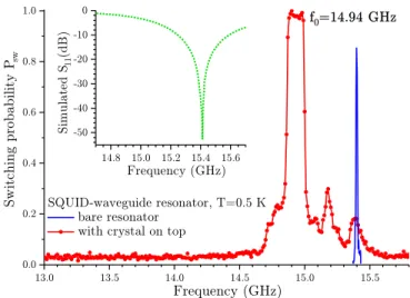
1 4 .8 1 5 .0 1 5 .2 1 5 .4 1 5 .6 -5 0 -4 0 -3 0 -2 0 -1 0 0 1 3 .0 1 3 .5 1 4 .0 1 4 .5 1 5 .0 1 5 .5 0 .0 0 .2 0 .4 0 .6 0 .8 1 .0 S i m u l a t e d S 1 1 ( d B ) Fr e que nc y ( G H z )
SQ U ID -wave guide r e sonat or , T= 0.5 K bar e r e sonat or wit h c r yst al on t op Fre q ue nc y (G H z ) S w i t c h i n g p r o b a b i l i t y P s w f 0 = 1 4 .9 4 G H z
FIG. 3. (color online) Psw of the SQUID at T =0.5 K under
microwave excitation as a function of frequency. The contin-uous line (blue) shows the scan of the bare resonator with a resonance frequency at 15.4 GHz, in good agreement with the simulations shown with dotted green line in the inset. When the resonator is loaded with a crystal, the resonance frequency shifts to f0 = 14.94 GHz as shown by the scan at
lower microwave power (red dots).
tively. If the magnetic flux change is larger than 1 2Φ0,
a feedback coil can be used to fix the SQUID’s working point and track the change of Isw28,29. Here, the flux
changes due to spin excitations are expected to be very small and the working point location in the plot of Fig.2 is essentially fixed by a normal static field arrising from an imperfect field alignement in the SQUID plan.
To verify the design, the SQUID Psw is measured
at T =0.5 K under microwave excitation as a function of frequency, with and without a crystal of Gd-doped CaWO4 placed on top of the chip. The CaWO4 has
a permitivitty35 ǫ
r ≈ 10 and therefore a shift of the
resonance frequency is to be expected when the crys-tal is placed on top of the chip. The blue line in Fig.3 shows the SQUID response in the case of an unloaded resonator with an estimated power at the chip entrance
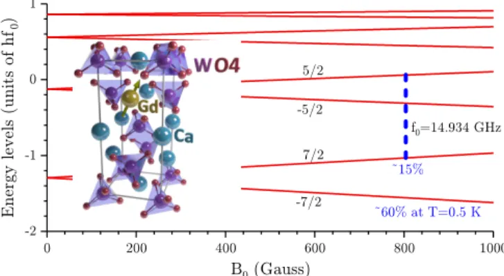
0 2 0 0 4 0 0 6 0 0 8 0 0 1 0 0 0 -2 -1 0 1 ~ 6 0 % a t T=0 .5 K -5 / 2 5 / 2 7 / 2 E n e r g y l e v e l s ( u n i t s o f h f 0 ) B 0 ( G auss) -7 / 2 f 0 =1 4 .9 3 4 G Hz ~ 1 5 %
FIG. 4. (color online) Gd3+ energy levels for B
0 applied
along the cristallographic c axis, corresponding to the z-axis of Hamiltonian H. The blue dashed line shows the studied transition. At T = 0.5 K and B0 = 804 G, the first excited
state Sz = 7/2 has a thermal population of ≈ 15%. The
inset shows the tetragonal symmetry of the CaWO4
crystal-lographic unit and a Gd3+spin (gold ball with an arrow).
of ≈ −10 dBm. Given the large amount of power, the bias current I has a low value of 45 μA, which allows to select the fundamental resonance at 15.4 GHz. The red dots show Psw for a loaded cavity and indicate a
reso-nance shift to f0 = 14.94 GHz. To show the versatility
of the device, in the loaded case, the power is reduced by 35 dB, which allows to operate at a higher bias cur-rent (329 μA). Outside the resonance, there are very few switching events (Psw ≈ 3%) likely due to thermal
ac-tivation. Under these conditions, other very low inten-sity modes are observed above 15 GHz. One notes that the SQUID is not shunted by a designated capacitance, the modes are independent on bias I and at a tempera-ture of 0.5 K one cannot observe SQUID’s internal level structure. During the ESR experiment, the microwave frequency is fixed at the main mode f0 = 14.934 GHz
and the external field can tune the spins in and out of resonance. The resonance is sufficiently broad to neglect in-plane field and microwave power induced shifts.
To confirm the cavity effect we have performed finite element simulations in COMSOL, in which we discretized the structure of the chip numerically and computed the values of the S-parameters as a function of frequency. The SQUID was simulated as a COMSOL lumped port defined between the Ω-loop and the ground metallic plane on which the Si chip is fixed. The port impedance defines the amount of absorbed energy and thus the resonance effect inside the waveguide structure. For the physical dimensions of the current device, the optimal value is
Zef f ≈ 142 Ω. The corresponding simulated frequency
dependence of S11 is given in Fig.3(inset) and it shows
a clear resonance at 15.4 GHz.
The spin Hamiltonian for the Gd3+ S = 7/2 ions
di-luted in CaWO4(tetragonal symmetry I4/a, see inset of
35 40 45 50 795 800 805 810 0.9 1.0 1.1 1.2 1.3 0 100 200 300 400 500 0.1 0.2 0.3 0.4 0.5 0.6 ( n s ) (b ) (c ) A m p l i t u d e A ( a r b . u n i t s ) Magnetic F ield (G ) (a ) 804 G fit 804 G S w i t c h i n g p r o b a b i l i t y P s w
Microwave pulse length (ns)
SQ U I D
puls e
M W puls e leng th
tim e
FIG. 5. (color online) (a) Psw as a function of microwave
pulse length at the resonance field 804 G. Continous lines are fits using exponential decays (see text). The inset is a sketch showing the timing of the microwave and the SQUID readout pulse (see text). Fit parameters τ (b) and A (c) as a function of B0. At resonance field 804 G, τ is maximum, while A has a
minimum, indicating resonant absorption of energy by spins.
Fig.4) is the following11:
H = gkµBSzB0+ B20O02+ B04O40+ B44O44+ B06O60+ B64O46,
(1) where B0 is magnetic field along the crystallographic c-axis, Ok
p are Stevens operators36, µB is Bohr
mag-neton, gk = 1.991 is the g-factor along the c−axis,
and the crystal field parameters are (in units of MHz)
B0
4 = −1.14, B44 = −7.02, B60 = 5.94 × 10⁻⁴ and B4
6 = 4.77 × 10⁻⁴. B02 has a detectable temperature
dependence37. Instead of a value11 of −894 MHz at
293 K, our data indicates that at 0.5 K, its value should be B0
2= −897.8 MHz. The obtained eigenvalues of H are
shown in Fig.4; the blue dashed line indicates the field lo-cation of the resonance Sz= 7/2 ↔ 5/2, at B0= 804 G.
The shift in frequency caused by the loading of the res-onator is larger than our expectations and no ground-state transitions fell within the appropiate experimental conditions. However, it is noteworthy that a success-ful measurement of such excited transition is relevant to show both the high sensitivity of the device as well as the potential of performing coherence control of multiple levels using this resonator and detection system.
At 6 K, the Gd spins have a typical relaxation time11 of the order of 10 ms and likely larger at our operating temperature of 0.5 K. Consequently the repetition fre-quency of the current pulse is decreased to 40 Hz to al-low some amount of relaxation between consecutive mea-surements. The microwave excitation can be applied in either CW or pulsed mode32. The end point of the mi-crowave pulse is chosen such that it barely overlaps with the micro-SQUID readout pulse, as sketched in the in-set of Fig.5(a). In this way, the SQUID can detect flux
4 changes due to spin rotation as well as energy
absorp-tion without saturating the SQUID readout. Once the overlap is fixed, the length of the microwave pulse can be varied by changing its start time, as indicated with a dashed left-arrow. For each length, the value of Psw is
obtained by repeating the shown pulses for 3,000 times and recording the percentage of SQUID switching events. The current SQUID pulse is fixed at ≈ 303 μA and 2.1 μs. A single crystal of Gd-doped CaWO4with dimensions
of 0.63 mm × 2.4 mm × 0.95 mm was placed over both shortcircuits shown in Fig.1such that the external mag-netic field is parallel to its c-axis (also z-axis) with a pre-cision of ≈ 2◦. Using dedicated direct-current and high
frequency electronics, the SQUID switching probability can be recorded as a function of temperature, magnetic field and microwave pulse characteristics. At T = 0.5 K, frequency f0 and power ≈ −10 dBm, Fig. 5(a) shows Psw vs. microwave pulse length tmw at the resonance
field B0 = 804 G. As tmw increases, the amount of
energy pumped in the SQUID increases and therefore
Psw increases up to a saturation level reached around
tmw ≈ 300 ns. The Psw(tmw) data is fitted with
func-tion Psw = C0− A exp−tmw/τ where C
0, A and τ are fit
parameters, as shown in Fig.5(a) with a continous line. The measurements are repeated with a 2 G step in the resonance region and the obtained A and τ parameters and their uncertainties are shown in Fig.5(b) and (c).
At the resonance field 804 G, the characteristic time
τ has a peak, while A has a dip, which are due to the
absorption of energy by resonant spins (slower satura-tion towards a smaller plateau). This indicates the res-onant absorption of microwave energy corresponding to the Sz = 7/2 ↔ 5/2 transition. The linewidth of the
resonance signal is about ∼4 G or 25 MHz in frequency units, which is a typical value for diluted spin systems (decoherence time of the entire spin ensemble T⋆
2 ≈40
ns). Spin-echo detection and Rabi oscillations at higher microwave powers are needed to characterize the decoher-ence time. The SQUID-waveguide device discussed here does offer the flexibility needed for such future studies.
The microwave pulse can excite only the spins situated in the very close proximity of the chip surface. The nu-merical simulations show that the microwave field inside the Ω-loop decays fast with height: from a surface value of 0.15 G (corresponding to an estimated -10 dBm input power in our experiments), the field halves at ∼11 μm above the chip. Due to the ∼μm size of the SQUID and the fast decay of the microwave field, the effective de-tected sample volume is estimated as in Ref. [27] to be ∼μm3size, which corresponds to ∼ 107 spins in the case
of the CaWO4:Gd3+ sample discussed here.
To perform Rabi oscillations with well-defined nutation rates, it is important to have an homogenous microwave field in the sample. This can be achieved by using very thin samples, which can be prepared, for instance, by chemical growth in 2D configurations, using radiation to generate defects or by cuting ultra-thin samples using a focused ion beam. Typical decoherence times T2 in
diluted spin systems are of the order of ∼ 1 − 10 μs9,11,
requiring Rabi frequencies of ∼ 10 MHz and microwave fields of several Gauss. Such values are attainable in future implementations of the technique presented here, by using higher microwave pulsed fields while operating the SQUID in its classical regime (T >∼ 0.1 − 1 K). It is expected that the signal size will actually increase due to population inversion generated by full spin rotation.
We present a sensitive on-chip detection scheme able to measure the first excited transition in a multi-level quantum spin system, at low temperatures. Gd spins S = 7/2 diluted in a CaWO4 crystal are in resonance with
the microwave excitation contained in a small volume around an Ω-shaped shortcircuit. A rough estimation of the number of detected spins is ∼ 107. This
SQUID-based resonator can be used in future studies to perform gated control of spin rotations.
This work was supported by the NSF Grant No. DMR-1206267 and CNRS-PICS CoDyLow. The NHMFL is supported by the Cooperative Agreement Grant No. DMR-1157490 and the State of Florida. We acknowl-edge support from the Strategic Priority Research Pro-gram of the Chinese Academy of Sciences (Grant No. XDB04000000). We are thankful to Dr. A. Tkachuk for providing the Gd sample and to X. Lian, S. Zhang and Dr. Xiong for the support in device fabrication.
1J. J. L. Morton and B. W. Lovett,
Annual Review of Condensed Matter Physics 2, 189 (2011).
2N. A. Gershenfeld and I. L. Chuang,Science 275, 350 (1997). 3S. Bertaina, S. Gambarelli, T. Mitra, B. Tsukerblat, A. M¨uller,
and B. Barbara,Nature 453, 203 (2008).
4A. Ardavan, O. Rival, J. J. L. Morton, S. J. Blundell,
A. M. Tyryshkin, G. A. Timco, and R. E. P. Winpenny,
Physical Review Letters 98, 057201 (2007).
5M. Shiddiq, D. Komijani, Y. Duan, A. Gaita-Ari˜no, E. Coronado,
and S. Hill,Nature 531, 348 (2016).
6K. Bader, D. Dengler, S. Lenz, B. Endeward,
S.-D. Jiang, P. Neugebauer, and J. van Slageren,
Nature Communications 5, 5304 (2014).
7F. Jelezko, T. Gaebel, I. Popa, M. Domhan, A. Gruber, and
J. Wrachtrup,Physical Review Letters 93, 130501 (2004).
8S. Bertaina, S. Gambarelli, A. Tkachuk, I. N.
Kurkin, B. Malkin, A. Stepanov, and B. Barbara,
Nature Nanotechnology 2, 39 (2007).
9S. Bertaina, L. Chen, N. Groll, J. Van Tol, N. S. Dalal, and
I. Chiorescu,Physical Review Letters 102, 050501 (2009).
10S. Nellutla, K.-Y. Choi, M. Pati, J. van Tol, I. Chiorescu, and
N. S. Dalal,Physical Review Letters 99, 137601 (2007).
11E. I. Baibekov, M. R. Gafurov, D. G. Zverev, I. N.
Kurkin, A. A. Rodionov, B. Z. Malkin, and B. Barbara,
Physical Review B 95, 064427 (2017).
12M. N. Leuenberger and D. Loss,Nature 410, 789 (2001). 13M. Blencowe,Nature 468, 44 (2010).
14I. Chiorescu, N. Groll, S. Bertaina, T. Mori, and S. Miyashita,
Physical Review B 82, 024413 (2010).
15D. I. Schuster, A. P. Sears, E. Ginossar, L. DiCarlo,
L. Frunzio, J. J. L. Morton, H. Wu, G. A. D. Briggs, B. B. Buckley, D. D. Awschalom, and R. J. Schoelkopf,
Physical Review Letters 105, 140501 (2010).
16H. Wu, R. E. George, J. H. Wesenberg, K. Mølmer, D. I. Schuster,
R. J. Schoelkopf, K. M. Itoh, A. Ardavan, J. J. L. Morton, and G. A. D. Briggs,Physical Review Letters 105, 140503 (2010).
T. Shimo-Oka, N. Mizuochi, K. Nemoto, W. J. Munro, and K. Semba,Physical Review Letters 111, 107008 (2013).
18A. Bienfait, J. J. Pla, Y. Kubo, M. Stern, X. Zhou, C. C. Lo,
C. D. Weis, T. Schenkel, M. L. W. Thewalt, D. Vion, D. Es-teve, B. Julsgaard, K. Mølmer, J. J. L. Morton, and P. Bertet,
Nature Nanotechnology 11, 253 (2016).
19C. Abeywardana, V. Stepanov, F. H. Cho, and S. Takahashi,
Journal of Applied Physics 120, 123907 (2016).
20N. Antler, E. M. Levenson-Falk, R. Naik,
Y.-D. Sun, A. Narla, R. Vijay, and I. Siddiqi,
Applied Physics Letters 102, 232602 (2013).
21A. J. Sigillito, H. Malissa, A. M. Tyryshkin, H. Riemann, N. V.
Abrosimov, P. Becker, H.-J. Pohl, M. L. W. Thewalt, K. M. Itoh, J. J. L. Morton, A. A. Houck, D. I. Schuster, and S. A. Lyon,
Applied Physics Letters 104, 222407 (2014).
22S. Baumann, W. Paul, T. Choi, C. P. Lutz, A. Ardavan, and
A. J. Heinrich,Science 350, 417 (2015).
23Y. Artzi, Y. Twig, and A. Blank,
Applied Physics Letters 106, 084104 (2015).
24W. Wernsdorfer, E. Bonet Orozco, K. Hasselbach, A. Benoit,
D. Mailly, O. Kubo, H. Nakano, and B. Barbara,
Physical Review Letters 79, 4014 (1997).
25W. Wernsdorfer, A. M¨uller, D. Mailly, and B. Barbara,
Europhysics Letters 66, 861 (2004).
26B. Cage, S. E. Russek, D. Zipse, J. M. North, and N. S. Dalal,
Applied Physics Letters 87, 082501 (2005).
27H. Toida, Y. Matsuzaki, K. Kakuyanagi, X. Zhu, W. J.
Munro, K. Nemoto, H. Yamaguchi, and S. Saito,
Applied Physics Letters 108, 052601 (2016).
28W. Wernsdorfer and R. Sessoli, Science 284, 133 (1999). 29L. Chen, W. Wernsdorfer, C. Lampropoulos, G. Christou, and
I. Chiorescu,Nanotechnology 21, 405504 (2010).
30L. Chen, H. Wang, X. Liu, L. Wu, and Z. Wang,
Nano Letters 16, 7726 (2016).
31P. W. Anderson and A. H. Dayem,
Physical Review Letters 13, 195 (1964).
32I. Chiorescu, Y. Nakamura, C. J. P. M. Harmans, and J. E.
Mooij,Science 299, 1869 (2003).
33J. Clarke and A. Braginski, eds.,The SQUID Handbook, Vol. 1
(Wiley-VCH Verlag GmbH & Co. KGaA, 2006) p. 409.
34V. Lefevre-Seguin, E. Turlot, C. Urbina, D. Esteve, and M. H.
Devoret, Physical Review B 46, 5507 (1992).
35E. S. Kim, S. H. Kim, and B. I. Lee,
Journal of the European Ceramic Society 26, 2101 (2006).
36K. W. H. Stevens,Proceedings of the Physical Society. Section A 65, 209 (1952). 37J. S. M. Harvey and H. Kiefte, Canadian Journal of Physics 49,