HAL Id: cea-01217062
https://hal-cea.archives-ouvertes.fr/cea-01217062
Submitted on 18 Oct 2015
HAL is a multi-disciplinary open access
archive for the deposit and dissemination of
sci-entific research documents, whether they are
pub-lished or not. The documents may come from
teaching and research institutions in France or
abroad, or from public or private research centers.
L’archive ouverte pluridisciplinaire HAL, est
destinée au dépôt et à la diffusion de documents
scientifiques de niveau recherche, publiés ou non,
émanant des établissements d’enseignement et de
recherche français ou étrangers, des laboratoires
publics ou privés.
Design of a full-silica pulse-compression grating
Nicolas Bonod, Jérôme Neauport
To cite this version:
Nicolas Bonod, Jérôme Neauport. Design of a full-silica pulse-compression grating. Optics Letters,
Optical Society of America - OSA Publishing, 2008, �10.1364/OL.33.000458�. �cea-01217062�
Design of a full-silica pulse-compression grating
Nicolas Bonod1,*and Jérôme Neauport21
Institut Fresnel, Aix-Marseille Université, CNRS, Domaine Universitaire de St. Jérôme, Case 161, 13397 Marseille, France
2
Commissariat a l’Energie Atomique (CEA) Cesta, BP2, 33114 Le Barp, France
*Corresponding author: [email protected]
Received November 27, 2007; revised January 11, 2008; accepted January 16, 2008; posted January 28, 2008 (Doc. ID 90214); published February 22, 2008
A diffraction grating engraved on a two-dimensional photonic crystal composed of square air holes in a silica matrix is numerically studied for the compression of ultrashort pulses. The silica is therefore the only solid material of the grating, and the reflection of the incident beam is based on the contrast of the air and silica refractive indices. This optical component enables the single use of silica as a solid material, presenting a high laser-induced damage threshold. In comparison to gratings engraved on a dielectric stack, multilayer dielectric, it offers the advantage of avoiding the presence of interfaces between two solid materials with different mechanical properties and sources of mechanical constraints that can distort the grating. © 2008 Optical Society of America
OCIS codes: 140.7090, 050.1950, 050.5298. Diffraction gratings are used in the compression of ultrashort pulses amplified by the so-called “fre-quency drift” method or chirped pulse amplification (CPA) [1]. Such diffraction gratings must offer a high diffraction efficiency to limit energy losses during pulse compression and a high laser-induced damage threshold (LIDT) since the incident beam has been previously amplified, generally by a laser-pumped titanium-sapphire crystal. Metal gratings can be used, but their low LIDT requires a high angle of in-cidence, and such gratings must therefore present a large surface area, resulting in disadvantages related to their weight and cost. Moreover, metal causes losses to the extent that the reflected efficiency is lim-ited [2]. Entirely dielectric gratings appeared in the mid-1990s [3] that made it possible to significantly increase the LIDT of compression gratings and to ob-tain measured reflected efficiencies close to 96% [4]. These diffraction gratings are engraved on a dielec-tric stack with two materials of high and low indices. Hafnium dioxide共HfO2兲 and silica dioxide 共SiO2兲 are
very frequently used. The disadvantage of this type of stacking lies in the presence of mechanical con-straints at the interfaces due to the different me-chanical properties of the two materials, which can deform the mirror and distort the spatial qualities of the beam and also considerably reduce the LIDT of the mirrors. Moreover, silica has very good resistance to the laser flow, but the other oxides frequently used, such as Ta2O5, HfO2, Al2O3, and TiO2, present a
much lower LIDT, which tends to reduce the damage threshold of the mirror [5].
To overcome these problems posed by dielectric stacks, this Letter presents a study of two-dimensional (2D) photonic crystals [6]. Air holes are made in a silica matrix, which then acts as the high-refractive-index material, whereas the air acts as the low-refractive-index material. These crystals avoid the use of a solid material other than silica and therefore eliminate the presence of interfaces be-tween two solid materials. The period of the photonic crystal is small enough such that the zeroth order is
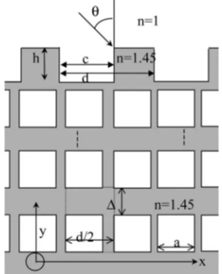
the only propagative order. The grating is engraved on the photonic crystal with a larger period than that of the photonic crystal, allowing the propagation of the first dispersive order. As a consequence, the pho-tonic crystal diffraction grating presents two differ-ent periods. The differdiffer-ential method is suited for modeling periodical devices so that the period of the diffraction grating on the Ox axis (see Fig.1) must be an integer of the period of the photonic crystal. In this Letter, the period of the diffraction grating is chosen to be twice that of the photonic crystal [7–9]. This Letter refers to the optogeometric parameters of the diffraction gratings used in the final stage of pulse compression of the PETAL project [10]. The wavelength is set at 1053 nm, the angle of incidence at 77.2°, polarization is TE, and the period d is 562 nm. Air holes in silica have a square cross section for numerical convenience, but a circular cross sec-tion would give similar results [11]. Their periodicity
Fig. 1. Two-dimensional photonic crystal composed of silica (in gray, refraction index n = 1.45) and air (in white, n = 1). Air holes have a square cross section. The binary grating has grooves with height h and width c and presents a period denoted d.
458 OPTICS LETTERS / Vol. 33, No. 5 / March 1, 2008
is fixed at one half of the periodicity of the grating, namely, 281 nm (Fig.1). The length of the sides of the squares is denoted a, and the thickness between the two layers of air holes along the Oy axis is denoted⌬. Calculations are performed by a numerical code based on the differential method [12]. Convergence is rapidly reached and ensured for all the results pre-sented in this Letter.
The first stage of the Letter consists of defining the geometry of the photonic crystal to guarantee its all-but-perfect reflectivity. The angle of incidence equal to 70.9° is set at the median angle between the two angles of diffraction of the first and zeroth orders of the diffraction grating that will be subsequently added to the photonic crystal [12,13]. The reflectivity of the crystal is thus calculated with respect to the length of the square cross section of air holes a and to the residual thickness⌬ of silica between two layers
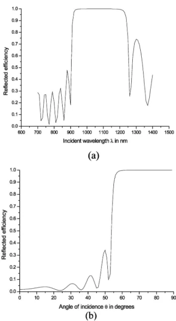
of air holes (see Fig.1). Air holes with a side length of 0.8 d allow an all-but-perfect reflectivity on a range of ⌬⬎100 nm (centered at ⌬=350 nm). The triangular and rectangular lattices give similar results. Six lay-ers of air holes are required to obtain a reflectivity of ⬎99% and ten layers ensure an all-but-perfect reflec-tivity 共⬎99.99%兲. Figures 2(a)and 2(b)show an ex-cellent reflectivity of the photonic crystal in a wide spectral interval (⬎99.9% over an interval of 200 nm) and high stability of the reflectivity according to the angle of incidence, given that the reflectivity is all but perfect for angles of incidence⬎60°.
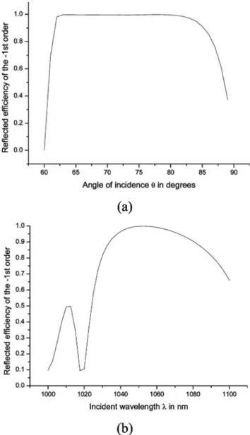
Reflected efficiencies in the first order are therefore studied as a function of the groove width and depth denoted as c and h, respectively, in Fig.1. It can be seen in Fig. 3 that these efficiencies can be numeri-cally very high over wide intervals of h and c. Let us now study the reflection efficiency in the first order according to the angle of incidence and the incident wavelength [Figs. 4(a) and 4(b)]. The reflectivity of the crystal is insensitive to the incident wavelength and to angles of incidence⬎60°, but the reflected ef-ficiency in the first order is dependent upon that through the presence of the grating. The total re-flected efficiency is always equal to 1, but part of the incident energy is diffracted in the zeroth order [9]. The angular tolerance is good, given that the re-flected efficiency in the first order is⬎99% in an in-terval of 18°. The spectral tolerance is comparable to that obtained with multilayer dielectric (MLD) grat-ings and is imposed by the profile of the grating. The distribution of the electric field in the upper part of the grating (Fig. 5) is similar to that observed in MLD gratings, as the field is concentrated in the grooves. An intensity enhancement can be observed at the right slope of the silica pillar, and recently it has been shown that the reduction of the pillar’s width permits reducing this intensity enhancement in the silica and increasing the LIDT of the grating [4,13]. Moreover, no reinforcement of the field at the interfaces between the air and silica is observed. Waddie et al. have shown that in the case of 2D pho-tonic crystals made of square HfO2 inclusions in a
SiO2matrix, the maximum of the electric field occurs
inside the HfO2inclusions, which increases the LIDT,
Fig. 2. Reflectivity of the crystal according to (a) the length of the incident wavelength and (b) the angle of in-cidence . Ten layers of air holes are in the silica. ⌬ = 350 nm, filling factor of 0.8, TE polarization; (a) = 1053 nm and (b) =70.9°. The refractive index of the silica is maintained constant and is equal to 1.45.
Fig. 3. Reflected efficiency of the first order as a function of the height h and width c of the grooves in nanometers. March 1, 2008 / Vol. 33, No. 5 / OPTICS LETTERS 459
compared to the MLD, where the maximum of the electric field occurs at the interface between HfO2
and SiO2[14]. However, it is not the case when
inclu-sions are made of low index material, as can be ob-served in Fig.5.
This Letter gives evidence that gratings composed solely of silica can offer reflected efficiencies in the first order ⬎99.9%. The reflectivity of the photonic crystal based on a contrast of refractive indices be-tween air and silica is all but perfect over wide spec-tral intervals and angles of incidence. These results are valid in TE polarization and cannot be repro-duced in TM polarization due to the poor reflectivity of the photonic crystal. Femtosecond laser microma-chining is the most adapted technique to manufac-ture 2D photonic crystals in silica [15]. Afterward, the grating shall be manufactured by a classical
ho-lographic process. Efforts are currently being made to manufacture what we believe to be the first small size prototype by this mean. Moreover, as a laser ma-chined and etched bare fused-silica device, our proto-type shall be fully compatible with a vacuum exposi-tion, as in pulse compressors.
References
1. D. Strickland and G. Mourou, Opt. Commun. 56, 219 (1985).
2. G. Loewen and E. Popov, Diffraction Gratings and Applications (Marcel Dekker, 1997).
3. M. D. Perry, R. D. Boyd, J. A. Britten, B. W. Shore, C. Shannon, and L. Li, Opt. Lett. 20, 940 (1995).
4. J. Neauport, E. Lavastre, G. Raze, G. Dupuy, N. Bonod, M. Balas, G. de Villele, J. Flamand, S. Kaladgew, and F. Desserouer, Opt. Express 19, 12508 (2007).
5. M. Mero, J. Liu, W. Rudolph, D. Ristau, and K. Starke, Phys. Rev. B 71, 115109 (2005).
6. K. Sakoda, Optical Properties of Photonic Crystals (Springer, 2001).
7. E. Popov, B. Bozhkov, and M. Neviere, Appl. Opt. 40, 2417 (2001).
8. D. Maystre, Opt. Express 8, 209 (2001).
9. N. Bonod, E. Popov, S. Enoch, and J. Neauport, J. Eur. Opt. Soc. Rapid Publ. 1, 06029 (2006).
10. N. Blanchot, G. Marre, J. Neauport, C. Rouyer, S. Montant, A. Cotel, C. Leblanc, and C. Sauteret, Appl. Opt. 45, 6013 (2006).
11. R. Padjen, J. M. Gerard, and J. Y. Marzin, J. Mod. Opt.
41, 295 (1994).
12. M. Neviere and E. Popov, Light Propagation in Periodic Medias: Differential Theory and Design (Marcel Dekker, 2003).
13. N. Bonod and J. Neauport, Opt. Commun. 260, 649 (2006).
14. A. J. Waddie, M. J. Thomson, and M. R. Taghizadeh, Opt. Lett. 30, 991 (2005).
15. V. Mizeikis, H. Sun, A. Marcinkevicius, J. Nishii, S. Matsuo, S. Juodkazis, and H. Misawa, J. Photochem. Photobiol. A 145, 41 (2001).
Fig. 4. Reflected efficiencies of the first order as a function of (a) the wavelength 共=77.2°兲 and (b) the angle of inci-dence 共=1053 nm兲. h=500 and c=340 nm.
Fig. 5. 兩E兩2 normalized by the incident field intensity in
the upper part of the grating over one period. The axes are in nanometers; h = 500 nm and c = 340 nm.