OATAO is an open access repository that collects the work of Toulouse
researchers and makes it freely available over the web where possible
Any correspondence concerning this service should be sent
to the repository administrator:
[email protected]
This is an author’s version published in:
http://oatao.univ-toulouse.fr/24654
To cite this version:
Parellada-Monreal, Laura and Castro-Hurtado, Irène and Martínez-Calderón,
Miguel and Presmanes, Lionel
and Mandayo, Gemma García Laser-induced
periodic surface structures on ZnO thin film for high response NO2 detection.
(2019) Applied Surface Science, 476. 569-575. ISSN 0169-4332
Laser-induced periodic surface structures on ZnO thin film for high response
N0
2
detection
L. Parella
d
a-Monreal
3•\
1. Castro-Hurtado
3•\M. Martfnez-Calder6n
3•\L. Presmanes
C,
G.G. Mandayo
a,
b,
*
• Celt, Manuel Lordlzdbal 15, 20018 Donostla/San Sebastldn, Spain
b Universldad de NaV01To, Tecnun, Manuel Lordlzdbal 13, 20018 DoMSlla/San Sebastldt!, Spain
• ClRIMA T, Universlti de Toulouse, CNRS, INPT, UPS, Toulouse Ceder 9, Fronce
ARTICLE INF O ABSTRA CT
Keywords: ZnO Femtosecond laser LIPSS Raman Gas sensor NO.
Femtosecond laser-induced periodic structures (LIPSS) have been processed on ZnO thin film gas sensor devices for nitrogen dioxide (NOi) detection. From the morphology point of view, the nanostructures have been iden tified as high spatial frequency UPSS (HSFL) with an average period of 145 nm. Through Raman analysis, a decrease of the typical wurtzite ZnO structure is shown, with a possible increase of defects such as Zn inter stitials. The response under N(½ is enhanced if compared with the only-annealed ZnO thin film for conœntra tions as low as 1 ppm, reaching 1 ppb of detection lirnit (WD) for the sensors with LIPSS. The Zn interstitials defects could be the source of the adsorbed N(½ species increasing the sensitivity. Reproducible results have been measured during 11 weeks in a row.
1. Introduction
Nanostructured materials presen t gpecial characteristics due to their small dimensions and morphologies, usually causing exceptional structural [1] and electrical [2] properties. Among others, these qua lities are useful for applications such as drug delivery [3], energy conversion [ 4] or chemical sensors [5]. Specifically on the sensing field, nanostructured materials have been widely investigated since the phenomena involved are based on surface reactions [6,7].
In the case of ZnO, shapes like nanoneedles, nanorods or hier archical structures have shown great responses to oxidizing gases, gpecially to N02 [8 10]. In this work, femtosecond laser induced per iodic structures (LIPSS) have been chosen to modify the sputtered ZnO surface for chemical sensor applications purposes.
LIPSS based nanopattems consist of a surface relief made of (quasi ) periodic lines, which exhibit a clear correlation to the wavelength and
polarization of the radiation [11]. Therefore, these structures are gen
erated when linearly polarized radiation interacts with a solid. Re cently, femtosecond LIPSS has proven its potential in patteming me
tallic materials [12], dielectrics [13], polymers [14] and thin films
[15].
Compared to traditional laser ablation techniques, femtosecond laser nano machining delivers extreme peak irradiance with minimal
thermal effects, offering the possibility of surface processing in open air atmosphere avoiding expensive vacuum technologies, while being free of chemicals and relatively fast. One of the most attractive properties of LIPSS based patterning is that is highly controllable, since it mainly depends on the material in use, the laser wavelength, À, the number of applied pulses per spot, N, the angle of incidence,
e,
and the polariza tion state of the laser electric field [16,17].In terms of nano structure periodicity, A, UPSS are divided into two main groups: the ones with A close to the irradiation wavelength are called low spatial frequency UPSS (LSFL), while structures with periods significantly smaller than À are referred to as high spatial frequency
UPSS (HSFL) [11,18].
The existence of HSFL allows for the generation of much smaller periods than LSFL, down to ~ )./4 - À/8, and although their origin is not fully understood and controversially debated in the literature [19,20], these structures have been obtained in a wide number of materials by carefully tuning the laser processing parameters. HSFL are formed at fluences very close to the damage threshold of the irradiated material and are oriented either parallel or perpendicular to the laser beam polarization, depending on the material [11].
As far as we are concemed, LIPSS have not been used as a crystal lographic and morphology modification for a possible enhancement of the gas sensing response. Due to the changes on the surface structure,
• Corresponding author at Ceit, Manuel Lardizabal 15, 20018 Donostia/San Sebastian, Spain.
E-mail address: ggmandayo@œites (G.G. Mandayo).
defects could be generated at the surface of the semiconductor and consequently a higher response could be expected for specific gases. Besides, the generation of LIPSS with a femtosecond laser presents an important advantage for gas sensing applications since the nanos tructures can be patterned directly on the sensing device (in situ),
without the need to transfer them, as it is the case of most of bottom up
techniques (ex situ) such electrospinning [21]or hydrothermal [22]
methods. On the other hand, this laser technique is able to nanos
tructure large surface areas [17], what is an important issue for its
application in industrial processes.
In particular, in this work, sputtered ZnO thin films, a semi
conductor that is well known as a sensitive layer for chemoresistive gas sensors, have been processed with a femtosecond laser in order to generate LIPSS on its surface. The device has been tested under dif
ferent atmospheres and specially under NO2, to study the nanos
tructures effect compared to only annealed thin films. 2. Experimental
2.1. Sensor fabrication
The fabrication steps of the ZnO sensing device are summarized in
Fig. 1. The sensor is based on a 1 × 2 cm2polished alumina substrate,
where a Pt heater was fabricated at the back side by photolithography
followed by DC sputtering in an Edwards ESM 100 system (Fig. 1(b)).
The lift off process was carried out with acetone. The same fabrication
steps were used to fabricate Pt interdigitated (IDT) electrodes with
50μm of separation and width on the top surface of the alumina
Fig. 1. Sensor fabrication steps: (a) alumina substrate, (b) Pt heater deposited on the back side of the alumina substrate, (c) Pt IDT electrodes deposited on top of the alumina substrate, (d) ZnO thinfilm layer deposited on top of the elec-trodes, (e) thermal treatment at 800 °C and (f) femtolaser processing.
Fig. 2. Schematic layout of the femtosecond laser machining setup for processing ZnO thinfilm at 800 nm.
Fig. 3. Optical image of the IDT Pt electrodes with the ZnO thinfilm on top. The dimensions of the LIPSS lines are not to scale with the rest of the image.
(Fig. 1(c)). In order to improve the adhesion of the metal to the sub strate, a 25 nm thick Cr layer was deposited for the subsequent 200 nm
thick Pt sputtering, both in the heater and in the IDT electrodes. 1 mm2
of ZnO sensing layer was deposited on top of the Pt IDT electrodes by photolithography followed by RF sputtering in an Argon atmosphere
(ZnO target 99.999% purity) under 5·103mbar of gas pressure in a
Pfeiffer Iontech system. The ZnO sputtering time was 1 h, the deposi tion temperature was between 21 °C and 23 °C and as for the Pt, acetone
was used for the lift off process (Fig. 1(d)). Afterwards, as shown in
(Fig. 1(e)), the sensor device was thermally stabilized in a quartz oven at 800 °C during 4 h in synthetic air (this process will be named TT800C). Finally, the femtolaser processing for the LIPSS generation
was performed (Fig. 1(f)).
The laser system used to generate the LIPSS on the ZnO surface was a Ti:Sapphire mode locked oscillator with a regenerative amplifier able to generate 130 fs pulses at a central wavelength of 800 nm with a
1 kHz repetition rate. The specific set up is shown inFig. 2. The laser
spot was focused on the ZnO samples utilizing a broadband 10× mi croscope objective with a numerical aperture (NA) of 0.16. Then, the spot size on the samples was measured using a 50× microscope ob jective and a Coherent LaserCam HR UV, yielding approximately a fo
cused spot diameter (ω0) of 6μm at 800 nm. Also, in the experiments of
this work, the focusing point was displaced certain distances yielding to
different values of the spot diameter (ωz) and consequently machined
line width[23].
In order to obtain the optimum laser parameters for LIPSS fabrica tion, different values of laser scanning velocity, pulse energy and spot
diameter were tested. The scanning velocity tested were 5μm/s, 10 μm/
s, 20μm/s and 50 μm/s, the pulse energies tested were 0.1 μJ, 0.5 μJ
and 1μJ and the spot diameters were varied from 6 μm up to 40 μm by
displacing the focusing point. These parameter combinations lead to the
fabrication of LIPSS with different morphologies that were character
ized via FEG SEM. Among all of them, using a pulse energy of 0.5μJ,
scanning speed of 10μm/s and the laser beam focused to aω0of 7μm
approximately, allowed us to fabricate the LIPSS nanopatterns with higher homogeneity and definition.
On the ZnO surface, two consecutive lines of LIPSS 900μm long and
separated 8μm were written between each IDT electrode as indicated in
red inFig. 3. The femtosecond laser processed only regions of ZnO thin
film deposited directly over the alumina substrate and not over the Pt
IDT in order to avoid alteration of the Pt/ZnO interface. 2.2. Film characterization
The ZnO thinfilm thickness, measured with a KLA Tencor profil
ometer, was around 180 nm.
To study the surface topography a JPK Nanowizard 3 Atomic Force Microscope (AFM) was used. Tapping Mode images were obtained using silicon Tap300 G cantilevers with a resonance frequency around
300 kHz and a tip with a radius<10 nm.
A Scanning Electron Microscope (SEM) Quanta 3D Field Emission Gun (FEG) system supplied by FEI Company was used to study the LIPSS morphology surface and in depth. The LIPSS periods were ana lyzed using the two dimensional Fast Fourier Transforms (2D FFT) of the FEG SEM surface images.
Raman spectra were collected under ambient conditions using
Horiba Jobin Yvon LabRAM HR 800 spectrometer equipped with afiber
coupled 532 nm laser. Spectra acquisition was carried out for 300 s using a ×100 objective lens and 1800 gr/mm grating. During the measurement, the resulting laser power at the surface of the sample was adjusted to 4 mW.
2.3. Electrical characterization
The electrical response characterization of the sensors under dif ferent gases was carried out inside a sealed stainless steel chamber. The
NO2, carbon momoxide (CO), benzene (C6H6), vinyl chloride (C2H3Cl)
and chlorine (Cl2) gases were taken from certified bottles mixed with
synthetic air (Air Liquide) in concentrations of 50, 100, 20, 10 and
15 ppm, respectively. In all the experiments a totalflux of 400 sccm was
used. The gas mixture in the chamber was obtained by a system con
sisting of a PC controlled massflow controllers (MFCs) Bronkhorst Hi
Tech. A DDE (Dynamic Data Exchange) communication is established
between the computer and the MFCs by Labview©.
The power consumption of the Pt heating element has been doubly calibrated with a thermographic camera and a Pt100 resistor, so the heater is power controlled by a voltage source. The conductance var iation of the sensing element was measured with a Keithley 2000
Multimeter, controlled by Labview©via GPIB.
The response of the sensors (SRx, where x is the name of the gas)
Fig. 4. (a) 2μm2AFM tapping mode images of ZnO TT800C on alumina, (b) 5μm2AFM tapping mode images of ZnO TT800C + LIPSS on alumina, (c) section profile
was calculated using the following definitions: =
SRx Gair/Ggas (1)
=
SRx Ggas/Gair (2)
for oxidizing and reducing agents respectively, where Gairis the con
ductivity of the sensor in air, and Ggasrepresents the sensor conductivity
after 30 min of gas exposure. The conductivity is defined as the inverse of the resistance.
3. Results and discussion
3.1. LIPSS nanostructuring characterization
From AFM and SEM images, a periodic structure can be observed in
Figs. 4(b) and5. The average period of the nanostructures extracted
from the 2D FFT is 145 nm and the average width of the processed lines
is around 7μm (Fig. 5). From the profiles of some AFM images
(Fig. 4(d)) a LIPSS depth around 100 nm is observed, while the average depth in the SEM cross section of the LIPSS is 140 nm. This mis matching between both measurements could be due to the fact that the
tip of the cantilever has a radius of curvature (r<10 nm) and pyramidal
shape, being unable to reach the bottom of the ZnO surface, implying an underestimation of the LIPSS height.
Taking into account the length and the approximate width of the
lines generated with LIPSS, a 12.5% of the total ZnO thinfilm surface
was processed.
The granular morphology and the size of the grains are preserved
under the LIPSS as can be appreciated inFig. 4(a) and (b) (it is worth to
notice that the AFM scanned areas have different size in each image). The average grain size is about 42 nm of diameter.
Fig. 5. (a) Schematic draw of the Pt IDT electrodes with the ZnO thinfilm on top. The red lines represent the LIPSS structures. (b) SEM image of one LIPSS line, (c) zoomed image of (b), (d) SEM image of a cross-section of the ZnO LIPSS processed by femtosecond laser and (e) zoomed image of (d).
In the specific case of ZnO nanostructuring via LIPSS, the existence
of HSFL and LSFL has been thoroughly analyzed by Pin Feng et al.[24].
In this work, the generation of HSFL with a periodicity of approxi mately 145 nm has been shown. This result is in agreement also with
the observations of X. D. Guo et al.[25,26]and M. Zamfirescu[27].
Regarding the stablished classification of HSFL in the work of J. Bonse
[11], we suggest that the fabricated structures consist in type HSFL 1
which are mainly observed in dielectrics and semiconductors with a period smaller than half of the incident laser wavelength and a depth of a few tens of nanometers.
Raman measurements were performed in order to investigate the crystallographic modifications between only annealed ZnO thin film
and ZnO with LIPSS. As shown in Fig. 6, the Raman peaks that are
common in both samples (378, 416, 430, 445, 576 and 645 cm−1) are
identified with the alumina substrate[28]. From the ZnO, it can be
observed that the peak around 436 cm−1vanishes for the ZnO with
LIPSS. This peak is identified with the optical phonon E2 mode and
attributed to the wurtzite crystal structure of ZnO[29], indicating that
on the LIPSS the wurtzite structure quality diminishes. This effect also
matches with the results shown by the team of X. D. Guo[25], where
ZnO nanostructures have been processed with a similar setup.
The sharp peak present in both samples at 576 cm−1is related to a
Raman mode of the alumina substrate, as mentioned before. However, there exists another very broad peak on the ZnO with LIPSS, between
518 cm−1and 594 cm−1, approximately (highlighted in blue square in
Fig. 6). A similar wide peak is shown in the Raman spectra of the LIPSS nanostructures generated by X. D. Guo with a maximum around
570 cm−1and they attribute it to ZnO A1(LO) phonon mode, related to
the defects of the nanostructures due to the laser irradiation. Never
theless, in the work done by G. J. Exarhos[29]on ZnOfilms is proposed
that a peak around 579 cm−1, identified with the E1(LO) mode, could
be related to defect electronic states within the bandgap due to an ex
cess of Zn content in thefilm. In the work of K. Saw [30], where
characterization of ZnO thinfilms is carried out, the same peak appears
wider (from 530 cm−1to 620 cm−1) and is also identified with the
same kind of defects and contrasted with X ray Photoelectron Spec troscopy (XPS) analysis. Besides, in the characterization of ZnO multi
layer nanosheets[31]a peak at 560 cm−1is related to Zn existence due
to incomplete oxidation. Therefore, it can be concluded that the wide peak that appears on the Raman spectra of the LIPSS nanostructures is related with defects, possibly due to Zn interstitials.
3.2. Gas sensing results
The detection principle of chemical gas sensors is based on the rise or decrease of the sensing material conductivity when it is exposed to reducing or oxidizing atmospheres. The sensing material needs to be heated up to temperatures around 200 °C 400 °C, where oxygen in the form of negatively charged species adsorbs on the surface of the semiconductor.
To demonstrate the sensing properties of the LIPSS generated on the
ZnO thinfilm, sensor devices with and without LIPSS were measured at
a typical detection temperature (325 °C) under 5 ppm of NO2, 50 ppm of
CO, 5 ppm of C6H6, 10 ppm of C2H3Cl and 1 ppm Cl2mixed with air.
Preliminary results showed that the only oxidizing gas tested, NO2,
presents the highest response for both type of sensors. InTable 1the
different SR
SR
NO x
2 ratios have been calculated, showing a very good se
lectivity to NO2, specially for TT800C + LIPSS, regarding the other
reducing agents.
Therefore, a deep study has been carried out with the NO2gas. In
Fig. 7, the response of both type of sensors at different temperatures are
shown for 2 ppm of NO2. As can be appreciated, the sensors with LIPSS
present responses much higher than non processed ZnO thinfilm, al
though the error bars are slightly bigger for all the temperatures in the case of the sensor processed by the femtosecond laser. All the error bars are calculated using four different measurements. Taking into account the abrupt increase in response around 350 °C, this temperature has been considered as the optimal temperature.
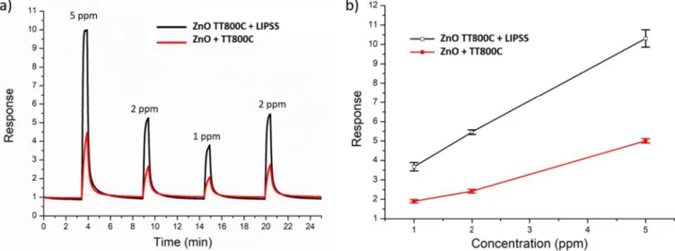
Afterwards, at the optimal temperature, the sensors were exposed to different concentrations in order to study the sensitivity of the devices (Fig. 8). For all tested concentrations (5 ppm, 2 ppm and 1 ppm) of NO2,
the sensor processed with LIPSS presents a higher response than the
ZnO thinfilm. In addition, repeatability of the response under 2 ppm is
tested, showing the same response at nonconsecutive pulses. In
Fig. 8(b), a linear sensitivity is shown for both sensors for concentra
tions between 5 and 1 ppm of NO2, so it can be calculated from the
slope of the straight line. The sensitivities are 1.7 and 0.8 ppm−1for the
sensor with LIPSS and without them, respectively. The detection limit (LOD) has been calculated using the following formula: LOD = 3σ /b where σ is the standard deviation of the base line during 5 min and b is the calculated sensitivity. For the sensor without LIPSS the LOD is al ready good: 3 ppb, but for the sensor with LIPSS, the theoretical LOD Fig. 6. Raman spectra of ZnO thinfilm annealed at 800 ° C compared with ZnO
thinfilm annealed at the same temperature with LIPSS.
Table 1
Ratios between the NO2response and the rest of the gases. SRNO SRNO 2 2 SRNO SRCO 2 SRNO SRC H 2 6 6 SRNO SRC H Cl 2 2 3 SRNO SRCl 2 2 TT800C + LIPSS 1 2.52 2.47 2.47 2.45 TT800C 1 1.70 1.57 1.62 1.64
Fig. 7. Response (SRNO2) of the ZnO sensors with LIPSS and without as a
downs to 1 ppb, showing up the possibility to use it in hazardous en vironments.
In order to study the repeatability of the sensors, pulses of 2 ppm of
NO2during 30 min have been carried out every week, during 4 weeks in
a row. After a month and a half with the sensors kept in the chamber open to ambient air and at the optimal temperature, the same experi
ment was performed and results are shown in Fig. 9. Both kind of
sensors present a repeatable behavior over all the tested period, with a
repeatability standard deviation (Sr) of 0.21 and 0.19 for the sensor
with and without LIPSS, respectively. The consequent repeatability
values (r = 2.3 ×Sr) are 0.48 and 0.44, respectively.
The responses showed for the sensor processed with LIPSS towards
low concentrations of NO2are similar or higher compared with other
published pure ZnO nanostructured sensors such as [32,22,33]. Al
though in the other works, the optimal temperatures are slightly lower than for the sensor with LIPSS, the fabrication techniques require sev eral steps avoided here by the in situ nanostructuring and selectivity is not shown in any of the investigations. Moreover, repeatability mea surements are rarely performed, leading to a lack of information and in this work we successfully demonstrate a good repeatability over more than two months, what is a key requirement for real applications.
During all the gas measurements performed at the optimal tem perature, the resistance baseline in the presence of air of the two type of sensors varied in the range of 20 kΩ 80 kΩ and 3 kΩ 18 kΩ for the sensor processed with LIPSS and for the sensors only annealed,
respectively.
Many conductometric NO2sensor devices have been tested during
the last decade, as it can cause severe respiratory diseases for long
exposures, but the NO2detection mechanism in semiconductors is still
under investigation[34].
Most of the proposed mechanisms are based on the importance of
the donor concentration defects, since can give electrons to NO2mo
lecules, decreasing the carrier density of the semiconductor. Two main
possible reactions are involved during the process[35,21]:
+ − ⇒ −
NO2( )g e NO2 (ads) (3)
+ − ⇒ + −
NO2( )g e NO( )g O(ads) (4)
where NO2in gas form reacts directly with the semiconductor surface,
generating adsorbed NO2species(3)or NO gas molecules and oxygen
species(4). Aside fromNO−
ads
2 ( ), other adsorbed NO2species could be
generated, as it is explained in[36], always through an electron given
from a donor defect to a NO2molecule with a simultaneous reoxidation
of an oxygen vacancy or Zn interstitial[37]. It is accepted that reaction
(3) occurs for temperatures lower than 250 °C and reaction (4)for
higher temperatures[35], therefore at the optimal temperature of the
sensors presented here, the reaction(4)should take place.
In ZnO nanoparticles, defects detected by photoluminescence (PL)
have been identified to contribute to the NO2 detection mechanism
[38]. More specifically, the group of M. Chen highlighted the effect of
donor defects as well as surface oxygen species[39,36]through in situ
diffuse reflectance infrared fourier transform spectroscopy (DRIFTS)
technique. As a result, it is proposed that the increase in response of the ZnO sensor devices with LIPSS nanostructures on it, compared with
only annealed ZnO thinfilm, could be a consequence of the increase of
the Zn interstitials defects on the ZnO surface, as Raman measurements suggest. As explained, the sensor processed with LIPSS present always a higher resistance than the only annealed sensor, what bears out the presence of more Zn interstitials. Therefore, as more donor defects,
more electrons will be transferred from the crystal to NO2molecules,
improving the sensitivity. 4. Conclusions
Generating LIPSS with a femtosecond laser on the ZnO surface is an innovative technique able to modify the surface morphology and the
defects at the material’s surface. This can be used as an advantage to
improve the sensitivity of conductometric gas sensing devices. In this work, ZnO HSFL nanostructures have been processed on Fig. 8. (a) Response (SRNO2) of the ZnO sensors with LIPSS and without at the optimal temperature (Topt.≃350 °C) for 5, 2, 1 and 2 ppm of NO2. (b) Sensitivity of the
two sensors at the optimal temperature.
Fig. 9. Repeatability of the responses (SRNO2) of both sensors under exposure of
[1] V. Roy, A. Djurišić, W. Chan, J. Gao, H. Lui, C. Surya, Luminescent and structural properties of ZnO nanorods prepared under different conditions, Appl. Phys. Lett. 83 (1) (2003) 141–143.
[2] E. Comini, V. Guidi, C. Malagù, G. Martinelli, Z. Pan, G. Sberveglieri, Z.L. Wang, Electrical properties of tin dioxide two-dimensional nanostructures, J. Phys. Chem. B 108 (6) (2004) 1882–1887.
[3] M. Goldberg, R. Langer, X. Jia, Nanostructured materials for applications in drug delivery and tissue engineering, J. Biomater. Sci. Polym. Ed. 18 (3) (2007) 241–268.
[4] A.S. Arico, P. Bruce, B. Scrosati, J.-M. Tarascon, W. Van Schalkwijk, Nanostructured materials for advanced energy conversion and storage devices, Nat. Mater. 4 (5) (2005) 366.
[5] X.-J. Huang, Y.-K. Choi, Chemical sensors based on nanostructured materials, Sens. Actuat. B: Chem. 122 (2) (2007) 659–671.
[6] S.R. Morrison, Semiconductor gas sensors, Sens. Actuat. 2 (1981) 329–341. [7] C. Wang, L. Yin, L. Zhang, D. Xiang, R. Gao, Metal oxide gas sensors: sensitivity and
influencing factors, Sensors 10 (3) (2010) 2088–2106.
[8] J. Gonzalez-Chavarri, L. Parellada-Monreal, I. Castro-Hurtado, E. Castaño, G.G. Mandayo, Zno nanoneedles grown on chip for selective NO2detection indoors,
Sens. Actuat. B: Chem. 255 (2018) 1244–1253.
[9] M. Jiao, N.V. Chien, N. Van Duy, N.D. Hoa, N. Van Hieu, K. Hjort, H. Nguyen, On-chip hydrothermal growth of ZnO nanorods at low temperature for highly selective NO2gas sensor, Mater. Lett. 169 (2016) 231–235.
[10] Y. Navale, S. Navale, N. Ramgir, F. Stadler, S. Gupta, D. Aswal, V. Patil, Zinc oxide hierarchical nanostructures as potential NO2sensors, Sensors Actuat. B: Chem. 251
(2017) 551–563.
[11] J. Bonse, S. Höhm, S.V. Kirner, A. Rosenfeld, J. Krüger, Laser-induced periodic surface structures—a scientific evergreen, IEEE J. Sel. Top. Quantum Electron. 23 (3) (2017) 109–123.
[12] M. Martínez-Calderon, M. Manso-Silván, A. Rodríguez, M. Gómez-Aranzadi, J. García-Ruiz, S. Olaizola, R. Martín-Palma, Surface micro-and nano-texturing of stainless steel by femtosecond laser for the control of cell migration, Sci. Rep. 6 (2016) 36296.
[13] E. Granados, M. Martinez-Calderon, M. Gomez, A. Rodriguez, S.M. Olaizola, Photonic structures in diamond based on femtosecond uv laser induced periodic surface structuring (LIPSS), Opt. Express 25 (13) (2017) 15330–15335.
[14] E. Rebollar, M. Castillejo, T.A. Ezquerra, Laser induced periodic surface structures on polymerfilms: from fundamentals to applications, Eur. Polym. J. 73 (2015) 162–174.
[15] A. Rodríguez, M.C. Morant-Miñana, A. Dias-Ponte, M. Martínez-Calderón, M. Gómez-Aranzadi, S.M. Olaizola, Femtosecond laser-induced periodic surface nanostructuring of sputtered platinum thinfilms, Appl. Surf. Sci. 351 (2015) 135–139.
[16] J. Bonse, J. Krüger, S. Höhm, A. Rosenfeld, Femtosecond laser-induced periodic surface structures, J. Laser Appl. 24 (4) (2012) 042006.
[17] I. Gnilitskyi, T.J.-Y. Derrien, Y. Levy, N.M. Bulgakova, T. Mocek, L. Orazi, High-speed manufacturing of highly regular femtosecond laser-induced periodic surface structures: physical origin of regularity, Sci. Rep. 7 (1) (2017) 8485.
[18] F.A. Müller, C. Kunz, S. Gräf, Bio-inspired functional surfaces based on laser-in-duced periodic surface structures, Materials 9 (6) (2016) 476.
[19] M. Huang, F. Zhao, Y. Cheng, N. Xu, Z. Xu, Mechanisms of ultrafast laser-induced deep-subwavelength gratings on graphite and diamond, Phys. Rev. B 79 (12) (2009) 125436.
[20] A. Borowiec, H. Haugen, Subwavelength ripple formation on the surfaces of com-pound semiconductors irradiated with femtosecond laser pulses, Appl. Phys. Lett. 82 (25) (2003) 4462–4464.
[21] M. Hjiri, L. El Mir, S.G. Leonardi, N. Donato, G. Neri, Co and NO2selective
mon-itoring by ZnO-based sensors, Nanomaterials 3 (3) (2013) 357–369.
[22] M. Procek, A. Stolarczyk, T. Pustelny, Impact of temperature and UV irradiation on dynamics of NO2sensors based on ZnO nanostructures, Nanomaterials 7 (10)
(2017) 312.
[23] J. Alda, Laser and Gaussian Beam Propagation and Transformation vol. 2013, (2003) pp. 999–1013.
[24] P. Feng, L. Jiang, X. Li, K. Zhang, X. Shi, B. Li, Y. Lu, Femtosecond laser-induced subwavelength ripples formed by asymmetrical grating splitting, Appl. Surf. Sci. 372 (2016) 52–56.
[25] X.D. Guo, R.X. Li, Y. Hang, Z.Z. Xu, B.K. Yu, H.L. Ma, X.W. Sun, Raman spectroscopy and luminescent properties of ZnO nanostructures fabricated by femtosecond laser pulses, Mater. Lett. 61 (23–24) (2007) 4583–4586.
[26] X.D. Guo, R.X. Li, Y. Hang, Z.Z. Xu, B.K. Yu, Y. Dai, B. Lu, X.W. Sun, Coherent linking of periodic nano-ripples on a ZnO crystal surface induced by femtosecond laser pulses, Appl. Phys. A: Mater. Sci. Process. 94 (2) (2009) 423–426,https://doi. org/10.1007/s00339-008-4838-y.
[27] M. Zamfirescu, M. Ulmeanu, F. Jipa, O. Cretu, A. Moldovan, G. Epurescu, M. Dinescu, R. Dabu, Femtosecond laser induced periodic surface structures on ZnO thinfilms, J. Laser Micro Nanoeng. 4 (1) (2009) 7–10.
[28] C. Bundesmann, N. Ashkenov, M. Schubert, D. Spemann, T. Butz, E. Kaidashev, M. Lorenz, M. Grundmann, Raman scattering in ZnO thinfilms doped with Fe, Sb, Al, Ga, and Li, Appl. Phys. Lett. 83 (10) (2003) 1974–1976.
[29] G.J. Exarhos, S.K. Sharma, Influence of processing variables on the structure and properties of ZnOfilms, Thin Solid Films 270 (1–2) (1995) 27–32.
[30] K.G. Saw, K. Ibrahim, Y.T. Lim, M.K. Chai, Self-compensation in ZnO thinfilms: an insight from X-ray photoelectron spectroscopy, Raman spectroscopy and time-of-flight secondary ion mass spectroscopy analyses, Thin Solid Films 515 (5) (2007) 2879–2884,https://doi.org/10.1016/j.tsf.2006.08.047.
[31] H. Fan, R. Scholz, F. Kolb, M. Zacharias, U. Gösele, F. Heyroth, C. Eisenschmidt, T. Hempel, J. Christen, On the growth mechanism and optical properties of ZnO multi-layer nanosheets, Appl. Phys. A 79 (8) (2004) 1895–1900.
[32] X. Wang, F. Sun, Y. Duan, Z. Yin, W. Luo, Y. Huang, J. Chen, Highly sensitive, temperature-dependent gas sensor based on hierarchical ZnO nanorod arrays, J. Mater. Chem. C 3 (43) (2015) 11397–11405.
[33] V.L. Patil, S.A. Vanalakar, P.S. Patil, J.H. Kim, Fabrication of nanostructured ZnO thinfilms based NO2gas sensor via SILAR technique, Sens. Actuat. B: Chem. 239
(2017) 1185–1193.
[34] A. Tamvakos, K. Korir, D. Tamvakos, D. Calestani, G. Cicero, D. Pullini, NO2gas
sensing mechanism of ZnO thin-film transducers: physical experiment and theore-tical correlation study, ACS Sensors 1 (4) (2016) 406–412.
[35] B. Ruhland, T. Becker, G. Müller, Gas-kinetic interactions of nitrous oxides with SnO2surfaces, Sensors Actuat. B: Chem. 50 (1) (1998) 85–94.
[36] M. Chen, Z. Wang, D. Han, F. Gu, G. Guo, High-sensitivity NO2gas sensors based on
flower-like and tube-like ZnO nanomaterials, Sensors Actuat. B: Chem. 157 (2) (2011) 565–574.
[37] M.-W. Ahn, K.-S. Park, J.-H. Heo, J.-G. Park, D.-W. Kim, K.J. Choi, J.-H. Lee, S.-H. Hong, Gas sensing properties of defect-controlled ZnO-nanowire gas sensor, Appl. Phys. Lett. 93 (26) (2008) 263103.
[38] F. Fan, Y. Feng, S. Bai, J. Feng, A. Chen, D. Li, Synthesis and gas sensing properties to NO2of ZnO nanoparticles, Sensors Actuat. B: Chem. 185 (2013) 377–382.
[39] M. Chen, Z. Wang, D. Han, F. Gu, G. Guo, Porous ZnO polygonal nanoflakes: synthesis, use in high-sensitivity NO2gas sensor, and proposed mechanism of gas
sensing, J. Phys. Chem. C 115 (26) (2011) 12763–12773.
sensor devices and tested under different gas atmospheres. A good se
lectivity towards NO2 gas is shown for both type of sensors compared to
CO, C6H6, C2H3Cl and Cl2. With only a 12.5% of the total ZnO area
processed with LIPSS, an increase of the sensor response of 50% (for
2 ppm of NO2 at 350 °C) is found in comparison with the only annealed
ZnO thin film sensor. The LOD downs to 1 ppb for the processed sensor, 3 times higher than for the sensor without LIPSS. With a femtosecond laser with a repetition rate of 1 MHz, instead of 1 kHz, an area of
20.000 μm2 could be processed in 0.28 s instead of 4.76 min, what
could be scalable to mass production.
Raman characterization reveals a decrease of the ZnO wurtzite structure for LIPSS, with an increase of surface defects such as Zn in
terstitials. Donor defects contribute on the NO2 detection mechanism,
releasing electrons to the oxidizing pollutants and consequently in creasing the sensitivity. Consequently, Zn interstitials are proposed as
the cause of the response enhancement for the tested NO2 concentra
tions.
Acknowledgements
Funding for this work was provided by the Ministry of Economy and
Competitiveness (MINECO) through the TEMIN AIR+ (project no.
TEC2016 79898 C6 3 R) and by the Basque Government under the
Elkartek program (MICRO4FAB grant no. KK 2016 00030). All the au
thors thank the technical and human support provided by Facility of Analysis and Characterization of Solids and Surfaces of SAIUEx UEx for the FIB measurements.