HAL Id: tel-01898865
https://tel.archives-ouvertes.fr/tel-01898865
Submitted on 19 Oct 2018
HAL is a multi-disciplinary open access archive for the deposit and dissemination of sci-entific research documents, whether they are pub-lished or not. The documents may come from teaching and research institutions in France or abroad, or from public or private research centers.
L’archive ouverte pluridisciplinaire HAL, est destinée au dépôt et à la diffusion de documents scientifiques de niveau recherche, publiés ou non, émanant des établissements d’enseignement et de recherche français ou étrangers, des laboratoires publics ou privés.
Boron-based nanomaterials under extreme conditions
Remi Grosjean
To cite this version:
Remi Grosjean. Boron-based nanomaterials under extreme conditions. Chemical Physics [physics.chem-ph]. Université Pierre et Marie Curie - Paris VI, 2016. English. �NNT : 2016PA066393�. �tel-01898865�
.
Université Pierre et Marie Curie
Ecole doctorale 397, Chimie et Physico-Chimie des Matériaux
Laboratoire Chimie de la Matière Condensée de Paris
Institut de Minéralogie, de Physique des Matériaux et de Cosmochimie
Nanomatériaux à base de bore
sous conditions extrêmes
Boron-based nanomaterials under extreme conditions
Par Rémi Grosjean
Thèse de doctorat en Science des Matériaux
Dirigée par David Portehault, Yann Le Godec, Corinne Chanéac
Présentée et soutenue publiquement le 17 Octobre 2016 Devant un jury composé de :
M. Bernard Samuel Directeur de recherche, CNRS Rapporteur
M. Machon Denis Maître de conférences, Université Lyon 1 Rapporteur
Mme. Laurencin Danielle Chargée de recherche, CNRS Examinatrice
M. Petit Christophe Professeur, Université Paris 6 Examinateur
M. Portehault David Chargé de recherche CNRS Co-directeur de thèse
M. Le Godec Yann Chargé de recherche CNRS Co-directeur de thèse
1
Ω
Δ >
) ¬ π
^ ´, )- ˇ•
∞ x (.) <> ∞
¿´ ∫ ◊ ~ ∂
≈ √ ]]
2
Remerciements
Bien qu’un seul nom figure sur la couverture du manuscrit, ce travail fut rendu possible par de nombreuses personnes.
Tout d’abord Clément, puis Florence qui m’ont accueilli au LCMCP, en stage puis en thèse, ainsi que Guillaume Fiquet, à l’IMPMC.
Je pense aussi à Patrick et Gervaise qui m’ont montré comment éteindre efficacement le TEM : en faisant entrer de l’air ; à Mohamed pour son aide avec les diffractos. Je remercie Isabelle pour les séances de MEB et la formation EDX. Je remercie bien sûr Cristina et Christel pour la RMN du noyau quadripolaire, j’aurais aimé avoir le temps de devenir utilisateur de niveau I.
Je pense à Tahar et Geeth, au LMV, qui m’ont permis de concilier expériences haute pression et visite de Clermont-Ferrand.
Je remercie Jean-Paul et Nicolas sur Psyché, qui nous ont confié la ligne, que nous avons consciencieusement noyée un soir d’ennui. Je remercie aussi Mohamed sur ID27, pour son guide de dépannage d’un fast-shutter par téléphone à toute heure du jour et de la nuit.
Pour leur patience devant les grilles de microscopie sans échantillon ou avec échantillon et pollution, je remercie Dario et Patricia.
Parce qu’il a toujours accepté avec plaisir mes paquets de vingt capillaires ou mes échantillons « urgents, parce que cette fois, c’est bon, on a la bonne phase », un grand merci à Ludovic.
Merci à Oleksandr pour son aide et les longues nuits passées dans les synchrotrons de France à contempler d’incompréhensibles signaux de diffraction.
Un grand merci aussi à Hélène et Corinne PdB qui ont toujours patiemment répondu à mes petites questions et qui ont rendu la vie au LCMCP plus facile, même quand un fournisseur veut envoyer ses avocats…
Pour toutes ses casquettes, merci au directeur de l’ED, ChrisBee. Merci pour avoir gravé dans ma mémoire les valeurs des spins nucléaires des isotropes du bore. Pour m’avoir rappelé que les vannes volent (parfois seulement) en rase-motte et qu’il existe plusieurs échelles de température, merci Olivier.
Je remercie Sophie Cas’ qui m’a fait entrer au labo et à l’école de la manipe robuste ! Aussi, merci à Sophie Car’ pour son aide et ses conseils, au long des 3 ans et pour les démontages successifs et remontages réussis de Baggy.
Le LCMCP c’est aussi les éphémères, coupables de l’ambiance de travail (et pas que) au labo, dont la liste est longue…
Merci à François, pour les anecdotes, à Hugo, à Johanna, à Benj (préjent), à Anne, à Xavier C, à Sam, à Xavier F, à Stan, à Manue, à Morgane, à Sarah, à Jérôme, à
3 Clément, à Lionel, à Claiiire, et tous les autres. Notamment, je pense à Virgile, «si ce n’est pas un ami, au moins un collègue ».
Parce que la rédaction se fait seul mais accompagné, merci aux compagnons de galère qui ont su rendre avant moi sans en faire trop. Je pense évidemment à Cez & Tidu-Tidu. Merci pour les échanges (à la raquette), le soutien technique Microsoft Office et tout le reste.
Pour le partage du C4-5, des fours, de la boîte à gants et de moult histoires et anecdotes, merci Tsou-Hsi Camille.
M. Gouge et Dr Gouget, Maître Artisan en sels fondus, inventeur du bore amorphe,
auteur de l’ouvrage « Le 5ème élément expliqué aux personnes âgées », dompteur de
vagues du Pacifique et chantre du Saint-Hilaire, mille mercis.
Simon pour m’avoir fait découvrir les températures supérieures à celles rencontrées en hiver à Dantzig en 1709 et à celle du sang de cheval. Et pour m’avoir appris dans quelle unité on les compte. Et pour avoir pris la relève.
Mille mercis à ma famille : mes parents, mes frères, tonton (alors, cette thèse ?), mes grands-parents, ainsi qu’à Jacky, Véro, Baptiste et tous les Mei-Alenda-Carnemolla-Marchi, tous plus patients les uns que les autres et prêts à entendre parler de bore et d’enclumes, encore. Et je ne remercierai pas Sophie M. Au 3 rue Thouin, à Budapest, à Lisbonne, à Bruxelles, en Dordogne, rue Erasme, 10 mètres sous la mer ou 30 cm sous la neige, les culs d’ours ont brillé par leur présence, leur soutien, leurs chansons parfois discutables, leur mauvaise foi. Merci
Jaul, Erwan, Eska, Aco, Jérem (préjent), Baddouf, Julie2, Belette, Matis, Samsam,
Flobert, JiRossugue. Et courage aux docteurs à venir. Et… place aux chefs !
Corinne, merci encore, pour l’accompagnement de la fin de la licence jusqu’à la fin de la thèse, pour ces réunions qui auront fait avancer le schmilblick (il est orange).
Il est d’usage de les nommer « encadrants ». A la fin de cette thèse, le terme ne me paraît pas adapté. David et Yann ont été deux véritables mentors : deux guides attentifs, sages. Yann qui m’a fait découvrir l’univers du GPa, le plaisir de l’usinage, les lignes de lumière, où nous avons noyé une ligne ou accumulé de nombreux diffractogrammes de la patafix. Merci pour ces soirées et week-ends passés sur la corrections du manuscrit. David, merci pour la science que j’ai apprise, la pas-science aussi (notamment la canalisation de mes innovations graphiques…), la patience, je promets de ne plus venir taper à la porte du bureau 10 fois par jour…
Last, but not least, je remercie « éventuellement » Nina, indéfectible soutien,
phare dans la tempête aux multiples facettes, tour à tour correctrice féroce et infatigable, inquisitrice des abus de langage et anglicismes, et bien plus. Bruce Wayne a Alfred Pennyworth, j’ai Nina, qui vaut bien plus d’un penny !
5
Table of contents
Abbreviation List ... 3
Introduction ... 9
References ... 19Chapter I: Bibliography ... 21
I-1- Nanomaterials & high pressure ... 23
I-1-1- Nanostructured high-pressure phases ... 24
I-1-1-a- Nanostructured diamond ... 26
I-1-1-b- Other nanostructured superhard materials: B-C-N system ... 32
I-1-2- Nanostructured materials under high-pressure ... 40
I-1-2-a- Oxides and related materials ... 40
I-1-2-b- Other materials ... 47
I-2- Boron: elemental forms and properties of the fifth element ... 50
I-2-1- Allotropes of boron ... 50
I-2-2- Stability of boron phases and phase diagram... 57
I-3- Boron-metal alloys: structure, properties and synthesis ... 59
I-3-1- Properties and structures ... 59
I-3-2- Synthesis and nanostructures ... 61
I-4- Conclusion ... 63
I-5- References ... 63
Chapter II: Synthesis of nanostructured precursors in molten
salts ... 69
II-1- Experimental set-up ... 71
II-2- Molten salts colloidal synthesis ... 74
II-2-1- Hafnium diboride ... 74
II-2-1-a- Synthesis in LiCl/KCl ... 74
II-2-1-b- Synthesis in LiI/KI ... 78
II-2-2- Calcium hexaboride ... 80
II-2-2-a- Synthesis in LiCl/KCl ... 80
II-2-2-b- Synthesis in LiI/KI ... 81
II-2-3- Nanostructured amorphous boron: nano Bam ... 83
II-3- Conclusions ... 91
II-4- References ... 92
Chapter
III:
HPHT
treatments
on
oxygen-containing
nanocomposites ... 93
III-1- Introduction ... 95
III-2- Experimental... 96
III-3- Results and discussion ... 98
III-3-1- Synthesis of metal borides-boron nanoparticles in molten salts .. 98
6
III-4- Conclusions... 107
III-5- Associated content ... 109
III-6- References ... 110
Chapter IV: HPHT formation of non-oxidised
nanocomposites ... 113
IV-1- Experimental set-ups ... 115
IV-2- Calcium hexaboride ... 117
IV-2-1- In situ XRD in Paris-Edinburgh cell ... 117
IV-2-1-a- Experiment at ID27/ESRF ... 117
IV-2-1-b- Experiment at PSICHE/SOLEIL Synchrotron ... 121
IV-2-2- Ex situ experiments ... 123
IV-2-2-a- Heating at 1350 °C ... 123
IV-2-2-b- Heating at 1550 °C ... 125
IV-2-2-c- Heating at 1750 °C ... 126
IV-3- Hafnium diboride ... 130
IV-3-1- In situ XRD in Paris-Edinburgh cell ... 130
IV-3-2- Ex situ experiments ... 133
IV-4- Conclusions & Prospects ... 138
IV-5- References ... 140
Chapter V: HPHT treatments of nanostructured amorphous
boron ... 141
V-1- In situ XRD in Paris-Edinburgh cell ... 144
V-2- Ex situ experiments ... 146
V-2-1- 5 GPa experiments ... 146
V-2-2- 14 GPa experiments ... 154
V-3- Conclusion and prospects ... 161
V-4- References ... 163
Conclusion ... 165
Appendices ... 171
1- Synthesis in molten salts ... 173
2- HPHT experiments ... 175
7
Abbreviation list:
The abbreviations used in this manuscript are defined here in the following. (HR)TEM: (High Resolution) Transmission Electron Microscopy
ABNNC: Aggregated Boron Nitride NanoComposite ADNR: Aggregated Diamond Nanorods
CVD: Chemical Vapour Deposition DAC: Diamond-Anvil Cell
DFT: Density Functional Theory
EDS: Energy Dispersive Spectroscopy EELS: Electron Energy Loss Spectroscopy
EXAFS: Extended X-Ray Absorption Fine Structure FFT: Fast Fourier Transform
HPE: Hall-Petch Effect
HPHT: High Pressure High Temperature HPT: High Pressure Torsion
ICP-OES: Inductively Coupled Plasma Optical Emission Spectroscopy ID: Internal Diameter
IMPMC: Institut de Minéralogie, de Physique des Matériaux et de Cosmochimie IR: Infra-Red
LCMCP: Laboratoire de Chimie de la Matière Condensée de Paris MAP: Multi-Anvil Press
MAS: Magic Angle Spinning
nano-Bam: SMS-derived nanostructured amorphous boron
NMR: Nuclear Magnetic Resonance NPD: Nano-Polycrystalline Diamond OD: Outer diameter
PDF: Pair Distribution Function POS: Partial Occupation of Sites
SAED: Selected Area Electron Diffraction SEM: Scanning Electron Microscopy SMS: Synthesis in Molten-Salts SPD: Severe Plastic Deformation
STEM-HAADF: Scanning Transmission Electron Microscopy -High Angle Annular Dark Field
STM: Scanning Tunneling Microscopy XPS:X-Ray Photoelectron Spectroscopy XRD: X-Ray Diffraction
9
11 Boron-based materials span a wide range of properties. This is illustrated by the widely spread use of boron oxide in the glass industry, as glass manufacturing and
fibre glass insulation represent around 75 % of boron use.1 Due to its strong reactivity
with oxygen, boron is naturally covalently bound to oxygen. In addition to boron oxide, numerous metal and alkaline borates are used for applications from fertilisers (sodium and calcium borates) to single-crystal optical components. Boron nitrides
h-BN and c-BN, isostructural to graphite and diamond, are also widely used
materials: h-BN finds applications as solid lubricant up to 900 °C, as ceramics or cosmetic products, while c-BN is used as abrasive in cutting tools for ferrous alloys in
which diamond is soluble at high temperature. Boron carbides such as B4C are also
used for their mechanical properties, in abrasive, wear resistant coatings or armour
plating. B4C is exploited in nuclear plants because of the large neutron capture
cross-section of boron.
Boron also makes alloys with a large variety of metals, the so-called metal
borides. These materials are used for their refractory properties, such as HfB2,
implemented as space-shuttle thermal shield for atmosphere re-entry. Metal borides
also exhibit interesting mechanical (TiB2), thermoelectric (HfB2), thermo-ionic
emission (LaB6) or superconducting properties (MgB2).2 The various properties of
metal borides stem from their numerous structures and stoichiometries, even for the same metal. Indeed, both boron and metal atoms usually have a formal null oxidation number, which emancipates metal borides from rules governing the structures of ionic compounds. For instance, Y-B alloys have various stoichiometries going from
YB2 to YB66. In metal borides, structural complexity is directly linked to the increase in
the boron content in the alloy: YB2 consists in yttrium atoms intercalated between
honeycomb boron layers, while YB66 has a complex face-centred cubic structure
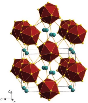
(a = 2.34 nm, 1584 atoms per unit cell) based on the B12 icosahedral building block.2
The B12 icosahedron is the common structural unit of boron-rich borides
(B/M > 12) and of all known boron allotropes. The elemental forms of boron remain challenging to both experimenters and theoreticians. Indeed, boron is the only stable element which ground state is still subject to debate, notably due to the difficulties encountered when calculating the relative energies of the modifications in
competition.3 Two new allotropes of boron have been discovered as recently as
2013.4 In 2014 and 2016, new elemental forms of boron were reported: full-boron
fullerene and two instances of 2-D boron base nanomaterials: borophene.5–7 In 2009,
the structure of an elemental modification of boron discovered in 1965 was solved.8,9
It is the only known elemental modification to exhibit actual charge separation, a
striking result.8,9 In addition, crystallisation of boron is made difficult by the extreme
sensibility of boron to the presence of foreign atoms. Indeed, numerous boron-rich borides (PuB100), carbides (B50C2) or nitrides (B50N2) have structures differing from
that of undoped-boron.3 Because of the strength of the boron-boron covalent bonds
and the complexity of the structures, the syntheses of most known boron phases are done under high pressure and temperature (HPHT) and the P,T phase diagram of boron is not set yet.4,8,10–12 Boron allotropes share common properties: they exhibit
12
strong chemical inertness, notably vs. oxidation, and very high hardness.8,10,13 The crystalline forms of boron are qualified of superhard materials, defined as solids
exhibiting a Vicker’s hardness superior to 40 GPa.14 As indication and to put boron
allotropes in perspective, the Vickers’ hardness of several materials is indicated in Figure 1.
Figure 1. Vickers’ hardness order of magnitude.
Hardness, as many inorganic materials’ properties, can be tuned according to the materials’ microstructure. Indeed, when the typical dimension matches the order of magnitude of physical phenomena, the resulting properties are modified. For instance, nanomaterials have specific properties in fields such as magnetism, optics or electronics. Moreover, nanostructuration of materials results in very high surface-to-volume ratio, hence enhanced reactivity, a particularly interesting feature for surface-based phenomena, such as catalysis or ion-insertion.
Compared to metal oxides, transition and noble metals, synthetic pathways towards nanostructured metal borides and boron phases remain poorly, if any, developed. Indeed, the covalent boron framework usually precludes crystallization below 400 °C, where instable and pyrophoric amorphous nanostructured borides are
obtained.2 Consequently, the synthesis of nanostructured metal borides must be
done at sufficient temperature to allow crystallisation but low enough to impede grain
growth, namely in the 400-1000 °C range.2 Recently, a general route toward
nanostructured metal borides has been developed: synthesis in molten salts (SMS).15
13 precursors of boron and metal and exploits the stability of molten inorganic salts in the temperature range considered. Recent works have evidenced the versatility of
this route, in terms of size and stoichiometry controls.2,15,16 Synthesis in molten salts
is the only known synthetic route that reaches sub-10 nm crystalline metal borides. A specific aspect of SMS-derived materials is their nanocomposite nature: the particles are embedded in a three-dimensional matrix, mainly composed of amorphous
elemental boron. Unlike previous works17,16,18, which focused on the particles’
properties and investigation of the underlying mechanism of SMS, the present PhD work aims at crystallising the amorphous matrix, while conserving (i) the borides particles and (ii) the nanocomposite nature of the material, using high pressure/high temperature (HPHT) processes.
Most recent developments of SMS have yielded a unique boron precursor:
nanostructured amorphous boron (patented).18 This material exhibits a unique
reactivity that has been investigated as additive in propellants used in spatial propulsion.19 In addition to its intrinsic properties, nanostructured amorphous boron represents a unique source of elemental boron for further synthesis and transformations. Along this PhD work, it has been used as starting material for boron crystallisation. As before-mentioned, high pressure and temperature are needed to achieve boron crystallisation.
Consequently, beyond the specific boron-based materials studied, this PhD work consists in the development of a synthetic methodology at the frontier between (i) liquid phase synthesis, (ii) nanosciences and (iii) synthesis in extreme pressure and temperature conditions.
High pressures are considered herein as exceeding 1 GPa. They are generated in the vast community of high pressure research using specific devices. Because the targeted field of this PhD work is materials synthesis, the devices chosen to explore high pressure conditions meet the requirement of high sample volume production with the compromise of high throughput experiments. Hence, two devices have been used: the Paris-Edinburgh press and the Kawai-type multi-anvil press. The pressures encountered with high pressure devices are described in Figure 2 and compared to those met in nature.
14
Figure 2. Pressure orders of magnitude.
A brief overview of the two set-ups used in this work is given below in order to provide the reader with key understanding of the experiments conducted in this work. A more detailed description is given in the appendices.
The Paris-Edinburgh and the multi-anvil press are hydraulic presses.20 An oil
pressure in the hundreds of bars range is applied to a first compression stage. The maximum pressure is reached between tungsten carbide anvils by successive surface reduction.
In the Paris-Edinburgh press, the sample is compressed between two tungsten carbide conical anvils (Figure 3), which design matches the shape of the gasket. The gasket contains the sample and the elements allowing heating. It also ensures that the pressure between the anvil is hydrostatic. The gasket is either made of pyrophyllite, for experiments dedicated to ex situ characterisation, or of amorphous boron and epoxy resin for in situ experiments monitored by X-ray diffraction. The sample is inserted inside a h-BN capsule (Figure 3). Heating is ensured by a resistive graphite heater. The temperature control is performed either using a thermocouple or based on power-supply output power vs. measured temperature calibration. In this press, it is possible to reach about 15 GPa and ca. 2000 °C. The reduced size and weight (ca. 50 kg for the instance in Figure 3) of this press allow easy installation on synchrotron or neutron beamlines.
15 Figure 3. (a) Paris-Edinburgh press, pencil for scale. (b) Tungsten carbide anvil. (c) High pressure assembly and gasket. (d) 3.5 mm assembly scheme. (e) Recovered sample after
experiment at 5 GPa, 10 cents coin for scale.
Multi-anvil apparatuses are much larger devices (Figure 4), in which the hydraulic pressure is transmitted to six steel outer anvils (Figure 4) then eight tungsten carbide cubic anvils. The tungsten carbide cubes are truncated on their vertexes, to form an octahedral cavity. The pressure chamber is usually a Cr2O3
-doped MgO octahedron, used as pressure-transmitting medium. By varying the vertexes truncation and the octahedron dimensions, various pressures can be attained (Table 1). Heating is also resistive and is either controlled directly with a thermocouple or based on previous power-supply calibration. A whole experimental set-up in a multi anvil press is schematised in Figure 5.
16
Figure 4. (a) 1500-ton hydraulic press at Laboratoire Magma et Volcans, Clermont-Ferrand. (b) Kawai-type multi-anvil system. (c) Various sizes octahedra.21
Table 1. Sample size according to the octahedron dimension. OEL is the octahedron edge length, TEL the anvil truncation edge length.21
OEL/TEL (mm) Capsule Volume (mm3) Maximum pressure (GPa)
25/15 2.4 8
18/11 1.8 11
14/8 0.67 15
Note that all the elements composing the high pressure assemblies (either for the Paris-Edinburgh or the multi-anvil press) are single-use and are either extruded along compression or cut to allow sample recovery.
17 Figure 5. Schematic preparation of a high-pressure experiment in a multi-anvil apparatus. (a) Cross-section of the pressure-cell octahedron (yellow rectangle: sample). (b) Ready-to-go octahedron. (c) Secondary anvils, consisting of eight truncated tungsten carbide
cubes. (d) Three inferior wedges, incorporating the eight cubes. (e) Superior wedges. (f) Containment ring. (g) Complete high pressure module with primary anvils (top and bottom
plates). (h) Uniaxial press.22
As described above, the experimental volume available in such devices is in the order of magnitude of the cubic millimetre. Consequently, they belong to the class of large-volume press, in opposition to the diamond-anvil cell (Figure 6), for which the sample size is a few hundred microns. Note that no experiment was conducted in diamond-anvil cells during this work, but it is the case for several studies presented in the bibliography.
Figure 6. Scheme of diamond-anvil cell (scale is not respected): the pressure chamber is 20 to 200 μm, total cell size is ca. 5 cm.21
The present manuscript aims at presenting the different steps performed within this PhD work to reach the goals mentioned above. To do so, the thesis is divided into five chapters, as follows.
23
appropriate diameter is drilled in the indentation centre. Material under investigation is placed in such a cylindrical void along with a ruby ball, which serves as a pressure gauge. The pressure chamber is then filled with neon which brings the conditions close to hydrostatic. Initial pressure could be as low as a few hundred bars (figure 1.3.1.3.1).
Figure 1.3.1.3.1 Diamond anvil cell scheme.
There are two major methods of heating in diamond anvil cells — laser and electrical one (Dubrovinsky et al. 2009; Dubrovinskaia & Dubrovinsky 2003) (figure 1.3.1.3.2).
Laser heating technique covers a wide temperature field: between 1300 and 5000 K. The sample preparation for laser-heating experiments is relatively easy and there is no practical risk to the diamonds due to heating (Dubrovinsky et al. 2009).
The other one is an external heating device that heats the whole diamond anvil cell. In this method thermal isolation of cell is required, e.g. aluminium foil. It covers temperature range 300-900 K with precision of 2 K. Temperature is directly measured by means of S-type Pt-Pt0.9Rh0.1 thermocouple.
18
Chapter I presents the bibliographic aspects of the project around three axes. First, the development of nano-materials using HPHT techniques is discussed, either for light element-based hard materials or oxides. Then, the different elemental forms of boron and their relative stability are discussed. Finally, the focus shifts to metal borides, their structure and the synthetic pathways reaching nanostructured metal borides.
Chapter II describes the synthesis of nanostructured materials using the synthesis in molten salts, by focusing on the advances reached in the course of this PhD work. Two types of materials have been synthesised: (i) nanostructured
crystalline metal borides (HfB2 and CaB6) obtained in a nanocomposite system as
they are embedded in a nanostructured amorphous matrix, and (ii) nanostructured amorphous boron.
Chapter III describes the results of HPHT treatments of the two nanocomposites, in the case of partial oxidation of the precursor’s matrix. This study shows the possibility to crystallise the matrix (into metal borates), while conserving the nanostructure of the system. The new nanocomposites boride/borates obtained also represent the first nanostructured instances of the two metal borates crystallised.
The focus of Chapter IV is HPHT treatments of the nanocomposite systems. In this case, the synthesis of the precursors has been optimised to limit matrix oxidation. The crystallisation of the matrix into non-oxidised phase is evidenced, notably in the light of in situ X-ray diffraction experiments on synchrotron beamlines. We demonstrate the successful synthesis of the first β-B/metal borides nanocomposites.
Eventually, Chapter V focuses on similar HPHT conditions but also higher pressures up to 10 GPa applied to nanostructured amorphous boron. The crystallisation of new nanostructured crystalline phases is established. Synthesis conditions are explored to establish the first speciation diagram originating from the transformation of nanostructured boron.
19
References
(1) Huppertz, H.; Keszler, D. A. In Encyclopedia of Inorganic and Bioinorganic
Chemistry; Wiley, 2014; pp 1–12.
(2) Carenco, S.; Portehault, D.; Boissière, C.; Mézailles, N.; Sanchez, C. Chem.
Rev. 2013, 113 (10), 7981–8065.
(3) Albert, B.; Hillebrecht, H. Angew. Chem. Int. Ed. 2009, 48 (46), 8640–8668. (4) Parakhonskiya, G.; Dubrovinskaia, N.; Bykova, E.; Wirth, R.; Dubrovinsky, L.
High Press. Res 2013, 33 (3), 673–683.
(5) Zhai, H.-J.; Zhao, Y.-F.; Li, W.-L.; Chen, Q.; Bai, H.; Hu, H.-S.; Piazza, Z. a; Tian, W.-J.; Lu, H.-G.; Wu, Y.-B.; Mu, Y.-W.; Wei, G.-F.; Liu, Z.-P.; Li, J.; Li, S.-D.; Wang, L.-S. Nat. Chem. 2014, 6 (8), 727–731.
(6) Mannix, A. J.; Zhou, X.-F.; Kiraly, B.; Wood, J. D.; Alducin, D.; Myers, B. D.; Liu, X.; Fisher, B. L.; Santiago, U.; Guest, J. R.; Yacaman, M. J.; Ponce, A.; Oganov, A. R.; Hersam, M. C.; Guisinger, N. P. Science 2015, 350 (6267), 1513–1516.
(7) Feng, B.; Zhang, J.; Zhong, Q.; Li, W.; Li, S.; Li, H.; Cheng, P.; Meng, S.; Chen, L.; Wu, K. Nat. Chem. 2016, 8, 563–568.
(8) Oganov, A. R.; Chen, J.; Gatti, C.; Ma, Y.; Ma, Y.; Glass, C. W.; Liu, Z.; Yu, T.; Kurakevych, O. O.; Solozhenko, V. L. Nature 2009, 457 (7231), 863–867. (9) Wentorf, R. H. Science 1965, 147 (3653), 49–50.
(10) Oganov, A. R. Boron Rich Solids; Orlovskaya, N., Lugovy, M., Eds.; NATO Science for Peace and Security Series B: Physics and Biophysics; Springer Netherlands: Dordrecht, 2011.
(11) Kurakevych, O. O.; Solozhenko, V. L. J. Superhard Mater. 2013, 35 (1), 60–63. (12) Ekimov, E. A.; Zibrov, I. P.; Zoteev, A. V. Inorg. Mater. 2011, 47 (11), 1194–
1198.
(13) Oganov, A. R.; Solozhenko, V. L. J. Superhard Mater. 2009, 31 (5), 285–291. (14) Wentorf, R. H.; DeVries, R. C.; Bundy, F. P. Science 1980, 208 (4446).
(15) Portehault, D.; Devi, S.; Beaunier, P.; Gervais, C.; Giordano, C.; Sanchez, C.; Antonietti, M. Angew. Chem. Int. Ed. 2011, 50 (14), 3262–3265.
(16) Gouget, G.; Beaunier, P.; Portehault, D.; Sanchez, C. Faraday Discuss. 2016. (17) Gouget, G. Approche moléculaire vers des nanomatériaux inorganiques
composés de bore : nouvelles nanostructures fonctionnelles, 2016.
(18) Portehault, D.; Gouget, G.; Gervais-Stary, C.; Sanchez, C. Matériau nanostructuré de bore amorphe, 2016, 15/55878
(19) Gouget, G.; Portehault, D.; Sanchez, C.; Beauchet, R.; Batonneau, Y.; Kappenstein, C. Mélange Energétique contenant du bore amorphe nanostructuré, 2016, Patent Pending
(20) Godec, Y. Le; Dove, M. T.; Redfern, S. A. T.; Tucker, M. G.; Marshall, W. G.; Syfosse, G.; Besson, J.-M. High Press. Res. 2001, 21 (5), 263–280.
(21) Parakhonskiy, G. Synthesis and investigation of boron phases at high pressures and temperatures, 2012.
21
23 The first chapter focuses on bibliographic aspects. More specifically, it is divided into three distinct parts, shedding light on the project’s different angles.
First, works dealing with the combination of nanostructured materials and high pressure treatment are discussed in an overview of the existing literature. Then, the interest shifts toward boron, its allotropes, their relative stability and their preparation conditions. Eventually alloys of metals and boron (metal borides) are briefly presented, considering their structure, properties and synthetic pathways toward nanostructured materials.
I-1- Nanomaterials & high pressure
First of all, both nanomaterials and what we consider as “high pressure” should be
defined. The commonly accepted definition, in agreement with IUPAC standards,1 of
a nanomaterial is a material for which one dimension at least is inferior to 100 nm. Consequently, 100 nm will be a cut-off size in the literature review. One should note that this size is not arbitrary. Indeed, nanomaterials properties arise from their high surface-to-volume ratio (S/V). The latter is a decreasing function of the particle size, as plotted in Figure I-1. It is clear here that under 100 nm the S/V ratio strongly increases, entering a S/V ratio domain where properties specific of nanomaterials emerge, such as catalysis or quantum confinement effects. Thus, it seems reasonable to restrain the study to sub-100 nm particles.
Figure I-1. Fraction of surface atoms plotted versus the diameter of a spherical particle.2
Concerning the pressure range, it is chosen to focus on studies conducted over 1 GPa. Two arguments justify this choice. Indeed, from atmospheric pressure
(10-4 GPa) to 0.8-0.9 GPa, the devices used differ thoroughly from those used above
1 GPa. Steel pressurised vessels generally do not operate over 1 GPa and over 500 °C. To go above 1 GPa until ca. 10 GPa, devices specifically designed for high pressure generation are used. Among them, one can cite the toroidal press, the Belt press, the piston-cylinder press, the multi-anvil press and the Paris-Edinburgh press.
24
Temperature can exceed 2200 °C in such devices. It is also interesting to note that above 1 GPa, pressure strongly reduces diffusion processes. Indeed, in first approximation, considering the following equation for self-diffusivity in a cubic crystal,
with 𝑫 the diffusion coefficient (Eq. I-1), where 𝑫𝟎 includes materials dependent
parameters (𝑫𝟎 = 𝒇𝒂𝟐𝛎𝟎, where 𝒇 is a correlation factor characterising self-diffusivity,
𝒂 the cell parameter and 𝛎𝟎 the attempt frequency) the diffusion coefficient 𝑫 is the
following (Eq. I-2).3,4 𝑫𝟎∗ also comprises the entropy term. Assuming P
1 is room
pressure and P2 is 1 GPa (Eq. I-3), the ratio between the corresponding diffusion
coefficient is at least 104 (Eq. I-4), making diffusion process extremely slow above 1 GPa in the absence of heating.
𝑫 = 𝑫𝟎𝒆(− △𝑮 𝒌𝑩𝑻) Eq. I-1 𝑫 = 𝑫𝟎∗𝒆 −(△𝑬+𝐏△𝑽) 𝒌𝑩𝑻 Eq. I-2 𝑷𝟐= 𝟏𝟎𝟒𝑷𝟏 Eq. I-3 𝑫𝟐 𝑫𝟏= 𝒆 (𝑷𝒌𝟏△𝑽 𝑩𝑻) −𝟏𝟎𝟒 Eq. I-4
Consequently, to reach similar diffusion coefficients, reactions and phase transformations occurring under high pressure call for higher temperature than their ambient pressure counterparts. The problem of diffusion limitation is of specific interest when dealing with nanomaterials. Indeed, being intrinsically metastable objects, sintering nano-objects (to increase the crystallinity, for instance) usually leads to grain growth and loss of nanostructure. Therefore, high pressure studies on nanomaterials can help maintaining the nanostructure and the benefits of thermal treatment. Moreover, nanostructuration of high pressure/high temperature (HPHT) phases also leads to properties improvement. Both aspects are discussed below.
I-1-1-
Nanostructured high-pressure phasesIn material sciences, the textbook case of HPHT phases is diamond. Both natural and commonly synthesised diamonds are made under pressure above 5 GPa and
over 900 °C. These diamonds are usually obtained as single crystals.5 Diamond is
commonly described has the hardest known material. However, these mechanical
properties are anisotropic and the Knoop hardness (Hk) varies from 60 to 120 GPa
depending on the crystallographic plane investigated and the direction of
measurement.6 Polycrystalline diamonds have been grown either by Chemical Vapor
Deposition (CVD) or with the help of a binder. CVD-grown polycrystalline diamonds have poor intergrain adhesion and their Knoop hardness does not exceed 100 GPa.
Using a binder such as cobalt7 allows the formation of sintered polycrystalline
diamond but at the price of hardness (Hk < 70 GPa) and thermal stability
25 The interest of getting binderless nanostructured polycrystalline samples of superhard materials lies a priori on several effects:
Decrease of the influence of anisotropy on mechanical properties5,8
Increase in thermal stability
Possibility to benefit from the Hall-Petch effect (HPE) (binders fill the inter-grains gap)
Increase of hardness by reduction of crystallite sizes, in agreement with
the HPE9,10
In relation with the latter point, it has been observed experimentally that grain boundaries limit dislocations in polycrystalline materials. This is mainly described using the concept of dislocation pile-up. Grain boundaries are barriers to dislocation motion, notably because of the crystallographic mismatch between adjacent grains. Therefore, upon stress application, dislocations concentrate in a grain until dislocation sources are activated in the neighbouring grain. Hence, reducing the grain size has a double effect. First, the number of grain boundaries per volume unit increases. Secondly, for each grain, the number of dislocations that can pile-up is reduced. Consequently, the amount of stress needed to propagate dislocations is increased compared to coarse-grained materials. At the macroscale, it means that the hardness is increased.
The relationship between the yield stress and the grain size d is described
by the Hall-Petch equation (Eq. I-5). Both k and 0 are both material-dependent
parameters, namely the strengthening coefficient and the friction stress in the absence of grain boundaries, respectively. They characterise the lattice’s resistance to dislocation.
𝞼 = 𝞼𝟎+ 𝒌
𝒅𝟐 Eq. I-5
However, this is not valid for all grain sizes.11 As plotted in Figure I-2, when grains are smaller than a critical value d* (corresponding to the golden arrow, typically around 10 to 20 nm), the hardness reduces, causing an inverse HPE. Above
d*, as the grain size is reduced, less and less dislocations can pile-up in a grain,
increasing the overall hardness. When the grain size is small enough, grains can accommodate only one dislocation, meaning the maximum of strengthening is reached. If the grain size is further decreased, below d*, other mechanisms are to be taken into account. If they are not entirely elucidated yet, recent studies suggest that
26
Figure I-2. Materials’ hardness as a function of grain size.11
The critical grain size d* would then correspond to a switch between creep and dislocation pile-up-based mechanisms as dominant fracture propagation
mechanisms. Based on Masumara and co-workers studies, Pande and Cooper11
proposed to generalise the yield stress applied to a polycrystalline material according to the following equation (Eq. I-6).
𝞼 = 𝞼𝟎+ 𝒌 𝒅𝟐+ 𝒌𝟏+ 𝑩𝟎 𝒅 + 𝑩𝒅 𝟑 Eq. I-6
The last three terms describe the diffusion-based dislocation transport. B0 and
k1 are constants and B a strain and temperature dependent parameter. For large
grain size, the first two terms are dominant, according to the HPE. For small sizes, the last three terms become dominant, leading to the inverse HPE. According to equation I-3, the critical value can be defined as the d value for which the first two terms are equal to the last three terms (Eq. I-7).
𝞼𝟎+ 𝒌
𝒅∗𝟐 = 𝒌𝟏+
𝑩𝟎 𝒅∗+ 𝑩𝒅∗𝟑
Eq. I-7
To conclude, it is possible to increase hardness by diminishing grain size, particularly when reaching the nanoscale, but not under 10-20 nm. This is particularly interesting in the case of bulk hard or superhard materials as it can yield improved properties and performances. The exploitation of the HPE has been successfully applied to superhard materials, first of which diamond, reaching nanopolycrystalline
diamond (NPD), as described by Irifune and co-workers and discussed below.5
I-1-1-a- Nanostructured diamond
The first report of NPD dates back to 1992, by Hodeau and co-workers.12 It was
obtained by compressing C60 at room temperature, over 20 GPa, under
non-hydrostatic pressures. However, due to small sample volumes (related to the use of diamond-anvil cells) and cell explosion upon decompression, the authors could hardly investigate the properties. Still, they were able to identify the crystalline phase obtained as cubic diamond, with a grain size comprised between 2 and 100 nm.
27 In 2003, Irifune et al. prepared binderless NPD by direct conversion from graphite, under high pressure and high temperature (at 12-25 GPa and in the 2300-2500 °C temperature range). Very high hardness values and high thermal
stability were claimed and more synthetic details were given in a further study.13
Materials were prepared in a multi-anvil apparatus, allowing larger sample volumes than diamond-anvil cells.
The results obtained according to the synthesis conditions are summarised in
(Figure I-3).13 X-Ray diffraction (XRD) measurements showed that only cubic
diamond is obtained over 2000 °C (Figure I-3).Transmission electron microscopy (TEM) observations show that the cubic diamond samples consist of 10-20 nm
crystals, randomly oriented, as evidenced by electron diffraction in the 2003 study.5
Along with these crystals, the samples also exhibit elongated crystals up to 200 nm long, consistent with rapid crystallisation of diamond or with the lamellar structure of initial graphite. Knoop hardness measurements were performed on the synthesised samples. At 18 GPa, 2500 °C for 1 min, transparent pure cubic diamond is obtained
with HK = 100-110 GPa. At 15 GPa, 2400 °C for 1 min, yielding also transparent pure
cubic diamond, HK = 130-140 GPa. At 12 GPa, 2000 °C for 5 min, opaque dark grey
pure cubic diamond is reached with HK = 65-95 GPa. Consequently, it is possible to
prepare NPD that possesses hardness at least equal to the one of single crystal
diamond (HK = 120 GPa maximum, in the appropriate crystallographic direction) and
even higher.
However, one must keep in mind that standardised hardness tests (such as Vickers or Knoop) are based on the penetration depth of a diamond tip with a specific geometry (as diamond is usually harder than the material to test). Therefore,
hardness values that exceed 120 GPa are to be taken with care.14
NPD prepared from graphite also has interesting stability properties compared to polycrystalline diamond with binders. The latter are stable only up to 600-700 °C under argon atmosphere, however NPD can be stable up to 1200 °C (under argon
28
Figure I-3. Left: Synthesis conditions of NPD and outcome. White dots correspond to cubic diamond, black dots to a mixture of cubic diamond, hexagonal diamond and compressed graphite. Asterisks indicate a grey and opaque product. Right: Powder XRD pattern of a sample
synthesised at 15 GPa and 2400 °C.13
The crystallisation of NPD from C60 has also been successfully obtained by
Dubrovinskaia et al., at 20 GPa and 2000 °C for 1h, using a multi-anvil apparatus and
hydrostatic pressures,15 independently of the cooling rate (Figure I-4). TEM and
HRTEM pictures show a particle size in the 5-12 nm range and confirm, along with electron diffraction, the cubic diamond structure. In some experiments, the authors report the presence of a small amount of 6H-diamond (based on XRD), which was
not observed with TEM. The HRTEM pictures of the NPD obtained from C60 suggest
that the structure is ideal and shows no stacking faults nor defects. The Raman spectra of diamond materials are shown in Figure I-4. The diamonds synthesised from natural diamond powder and graphite have spectra dominated by the sharp peak at ca. 1330 cm-1. The bands at 500, 1100 and 1420 cm-1 are attributed to a rupture of selection rules due to small crystallite size. It is clear from Raman spectroscopy that NPD’s properties are influenced by the precursor used. However, the authors insist that they have no complete explanation for the features of the NPD Raman spectra.
29 Figure I-4. Characterisations of NPD synthesised from C60 at 20 GPa and 2000 °C. (a)
and (b): (HR)TEM pictures of NPD synthesized from C60, evidencing 5-12 nm particles of cubic
diamond with ideal structure. (c) Electron diffraction pattern, evidencing the cubic diamond phase. (d) Raman spectra of different diamond materials, synthesised at 20 GPa and 2200 K.
Red line: synthesis from C60. Blue line: synthesis from graphite. Green line: synthesis from
natural diamond.15
The mechanical properties of the NPD obtained from C60 were tested with a
standard Vickers-type diamond indenter. Even for important loads (4.9 N) and using a scanning electron microscope (SEM), the indenter left no visible mark on the sample, suggesting a hardness at least comparable to that of bulk diamond.
The thermal stability under inert atmosphere was also tested. Natural diamond
and NPD (from C60) were heated at 1900 K under an atmosphere composed of
Ar+2% H2. For natural diamond, graphitisation started at 1100 K and became rapid at
1500 K. However, NPD synthesised from C60 did not graphitise at 1800 K and started
at 1900 K, exhibiting superior thermal stability compared to natural diamond.
The authors also obtained aggregated diamond nanorods (ADNR) by treating
C60 at 20 GPa and 2200 °C.16 After 1 h, the reaction medium was slowly cooled
(ca. 10 °C/min). The XRD pattern and the Raman spectra are similar to that obtained for NPD. HRTEM shows (Figure I-5) that diamond is obtained as rods, which length can be superior to 1 m and width is inferior to 20 nm. As evidenced by TEM, the rods are randomly oriented (Figure I-5). Both electron and X-Ray diffraction were
30
used to measure the lattice parameter, which is 3.5617(3) Å, making nanorods 0.2 to
0.4 % denser than bulk diamond (3.528(1) g.cm-3 vs. 3.515-3.519 g.cm-3 for bulk
diamonds). The equation of state was determined, particularly the isothermal bulk modulus, which exceeds that of known materials (491 GPa, about 10 % more than that of natural diamond). Consequently, ADNR represent the densest and least
compressible form of carbon. The mechanical properties were tested elsewhere.17
The Young’s modulus (1070 GPa) is comparable to that of natural diamond (ca. 1130 GPa). The Knoop hardness measurements give 57 to 104 GPa for natural diamond, depending on the indentation plane, but at least 105 GPa for ADNR, independently of the direction investigated. The wear coefficient, useful in order to consider applications as machining tool for instance, equals 2.14 to 5.49 for natural diamond and 10 for ADNR. The fracture toughness is also greatly increased
(3.4-5.0 MPa.m2 for natural diamond, 11.1 MPa.m2 for ADNR). The efficiency of ADNR as
grinding tool was tested, particularly with ferrous steel. Indeed, diamond tends to form iron carbide and cannot be used to grind ferrous alloys. When grinding stainless steel with either ADNR or natural diamond (Figure I-5), the authors showed that no etching could be seen on ANDR sample, suggesting higher stability toward reaction with ferrous alloys, making ADNR a very promising product for machining and cutting tools.
Figure I-5. Left: TEM image of ANDR, showing randomly oriented crystals. Middle: ADNR bulk sample after grinding test on stainless steel. Right: Natural diamond sample after
grinding test on stainless steel, the yellow arrow highlights the etching spot.
Both synthesis conditions of nanopolycrystalline diamond from different carbon forms and the resulting mechanical properties have been summed up by Irifune and co-workers (see Table I-1).18,19
Table I-1.NPD synthesis conditions, particle size and materials’ hardness.
Starting Material Synthesis Conditions Outcome (XRD) Particle size (TEM, nm) Knoop Hardness (Gpa) Graphite 15 GPa, 2400 °C, 78 s c-Dia 10-30 (lamellar) 128-138 Graphite 28 GPa, 2500 °C, 10 s c-Dia 98% + h-Dia 10-30 (lamellar) 120-140 Graphite 21 GPa, 2300 °C, 10 min c-Dia 10-30 (lamellar) 113-139 Amorphous-C 18 GPa, 2000 °C, 20 min c-Dia 10-200 97-119 Amorphous-C 21 GPa, 1800 °C, 10 min c-Dia 5-10 70-74
31 NPD was also prepared from graphite by Xu et al., who studied the influence
of graphite ball-milling before HPHT.20 They compared NPD obtained either from
crystalline graphite or ball-milled and/or heated under vacuum after milling. Ball-milling is used to reduce the crystallite size of the precursor. Reducing the initial grain size tends to reduce, at the same pressure, the thermal energy needed to crystallise diamond. As suggested by Guillou and co-workers, NPD nucleation and growth does not require graphitisation of disordered carbons. However, the particle size was only calculated by applying Scherrer’s formula to the XRD patterns and no TEM observations were provided to confirm the particle size of NPD synthesised from
ball-milled/vacuum heated graphite.21 As emphasised by Guillou et al., the rapid
formation of diamond results in twinning and high residual strains after recovery, which contribute significantly to broadening of the XRD peaks. Consequently, in the absence of TEM pictures, it is difficult to assess the influence of the pre-HPHT treatment of graphite on the NPD grain size. The mechanical properties were tested under a Vickers’ indenter which broke under a 20 N load without indenting the material.
As discussed above, the properties of NPD make them a potentially very useful material for applications involving cutting or machining. From a different angle, diamond’s hardness is also used for static pressure generation devices, namely diamond anvil cells. NPD were successfully used as anvils.22 For large culet sizes (i.e. the dimension of the flat bottom part of a gemstone, here corresponding to the pressure generating surface), NPD anvils can generate 1.5 to 2 times the pressure
generated by single crystal diamond anvils.23 Concerning laser-heating, it is possible
to generate up to 5000 K at 100 GPa.22 The increase in heating efficiency compared
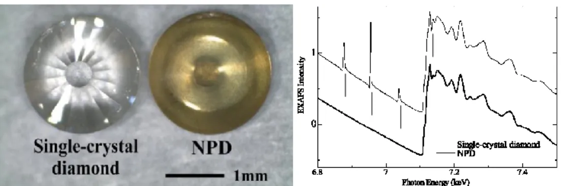
to single crystal diamond is linked to the lower thermal conductivity of NPD, paving the way toward performance increase in diamond anvil cells. In addition, NPD-based anvils are especially useful for EXAFS in situ studies: unlike single-crystals diamond anvils, NPD anvils do not exhibit Bragg reflections that otherwise superimpose the spectrum (Figure I-6).24
Glassy-C 21 GPa, 2250 °C, 6 min c-Dia 50-200 95-112 Glassy-C 18 GPa, 2000 °C, 20 min c-Dia 5-10 66-86
C60 18 GPa, 1800 °C, 30 min c-Dia 5-10 70-85 C60 18 GPa, 2000 °C, 35 min c-Dia 20-100 93-104
Ref: Natural diamond 110–135 (001)
c-Dia: cubic diamond h-Dia: hexagonal diamond
32
Figure I-6. Left: diamond anvils. Right: comparison of EXAFS spectra according to the anvil type.24
On a more general point of view, superhard materials are often based on light elements, such as boron, carbon or nitrogen. Indeed, they make usually strong, short
and directional covalent bonds responsible for high hardness, such as B13N2 or
B6O.25 For some of these materials, nanostructured occurrences were prepared
using HPHT techniques. They are detailed in the following part.
I-1-1-b- Other nanostructured superhard materials: B-C-N system • Cubic boron nitride
Among intrinsically superhard materials, besides diamond, cubic boron nitride is usually cited. Indeed, it is isoelectronic to carbon and the most common phase, hexagonal boron nitride (h-BN), has a graphitic structure. As for carbon, a denser phase is stabilised at high pressure: cubic boron nitride (c-BN), discovered in 1957, which exhibits high hardness (HV = 45 GPa).26 Even if it is much less hard than
diamond, c-BN exhibits higher thermal and chemical stability. This makes c-BN a more suitable material for cutting ferrous alloys, for which single crystal diamond is not suited.
Recently, Dubrovinskaia and co-workers reported the synthesis of aggregated
boron nitride nanocomposites (ABNNC).27 The temperature/pressure diagram in
Figure I-7 sums up the results they obtained according to the synthesis conditions.27
The XRD patterns obtained for P = 18 GPa evidence the different phases obtained and their mixture, as a function of the synthesis temperature. w-BN, wurtzititic boron nitride, is also obtained. It is another high pressure superhard phase of boron nitride, but with a lower thermal stability. Its structure is similar to that of hexagonal diamond.
Figure 1. Photograph of diamond anvils. Figure 2. EXAFS spectra obtained with
single-crystal diamond anvil and NPD anvil.
In this paper, magnetic EXAFS at high pressures is presented for fcc Fe65Ni35 Invar alloy, in which the
DAC with NPD anvils was employed for the first time. Fe and Ni metals were also measured at ambient pressure as reference materials in bcc and fcc structures. Fe-Ni Invar alloy has been regarded as a prototypical material that exhibits anomalously low thermal expansion [4]. Because the magnetic EXAFS is element-specific and electronic-shell selective, it is appropriate for comparing Fe and Ni atoms in the local environment.
2. Experiment
X-ray absorption and dichroic spectra were recorded at the Fe and Ni K-edges using the helicity-modulation method on beamline 39XU at SPring-8 [5], which was equipped with a diamond 111 double-crystal monochromator, Kirkpatrick-Baez focusing mirrors [6], and a diamond λ/4-plate to produce a circularly polarized beam. A magnetic field of 0.6 T was sufficient to magnetically saturate the sample. The generated pressure was estimated by the ruby fluorescence method. Two kinds of diamond anvil, single-crystal and nano-polycrystalline diamonds are compared in the photograph in figure 1. Although the NPD exhibits a dark yellow due to nitrogen impurities and lattice defects [7], it has a high transparency for X-rays. Figure 2 shows the raw EXAFS spectra of Fe metal recorded using the DAC with single-crystal diamond and NPD. The latter gives a much better spectrum without any spikelike noise. We succeeded in recording a glitch-free spectrum with a high accuracy over a wide range of photon energy (6 - 10 keV). The experiment was carried out at room temperature.
Figure 3. EXAFS spectra at the Fe K-edge (left
panel) and Ni K-edge (right panel) in Fe-Ni invar alloy, Fe and Ni foils.
Figure 4. Pressure variation of RDF for Fe and
Ni absorbing atoms.
23rd International Conference on High Pressure Science and Technology (AIRAPT-23) IOP Publishing Journal of Physics: Conference Series 377 (2012) 012039 doi:10.1088/1742-6596/377/1/012039
33 Figure I-7. Left: P,T diagram of commercial pyrolytic BN HPHT transformations. The region under the solid line is where the starting material is present in the final product. Above
the dashed line, only c-BN is obtained, as a polycrystalline bulk. The shaded region corresponds to the samples with the smallest grain size, around 14 nm, and highest hardness.
Right: Powder XRD patterns for samples prepared at 18 GPa.27
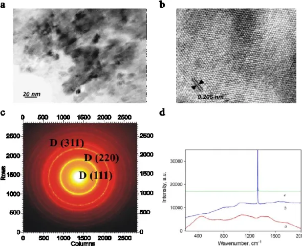
At 18 GPa and 1870 K, TEM and electron diffraction (Figure I-8) show a good agreement with the XRD data: both c-BN and w-BN are obtained, as 14-20 nm nanoparticles.
Figure I-8 TEM picture of the sample synthesised at 18 GPa and 1870 K. The mixture of
c- and w-BN is obtained as 14 nm nanoparticles. The particles consist in blocks with 2-layered w-BN and 3-layered c-BN structures, as evidenced by the TEM picture (upper right corner). The
corresponding SAED pattern is shown in the lower left corner.
For aggregated w-BN/c-BN nanocomposites, the hardness value reaches a maximum of Hv = 85 GPa for a 14 nm crystallite size. Below this critical size, the
inverse Hall-Petch effect applies. However, the samples with grain size below 12 nm were synthesised at 1800 K, the authors suppose than the final material may contain
34
residual amounts of pyrolytic (p-BN) that they hold responsible for the hardness decrease.
For applications in machining tools, thermal stability is important, as high-speed machining of hard materials tends to release heat. Yet, w-BN is a metastable
phase that undergoes reverse transformation to h-BN at moderate temperatures,28
thus yielding significant hardness decrease at high temperature for the w-BN/c-BN nanocomposites. Further enhancement of boron nitride properties as superhard material through nanostructuration should then avoid the presence of w-BN in the final material. The precursor, p-BN, consists in graphitic BN planes, ordered in the two dimensions of these planes. The planes are randomly oriented in respect to each other: p-BN exhibits no three-dimensional ordering. However, commercial p-BN samples do have a certain degree of ordering in the third dimension: the structure is not entirely turbostratic; some domains have h-BN structure. This is precisely in such domains that the crystallisation of w-BN is favoured, while that of c-BN occurs in
more disordered domains.28,29
To avoid the presence of w-BN, Le Godec and co-workers used high purity
p-BN without any three dimensional ordering, synthesised by CVD.28 Syntheses at 12 GPa show that w-BN still appears at 1000 K, c-BN becoming the sole crystalline phase only above 2000 K. The hypothesis here is that at low pressures, temperature-induced ordering of the initial p-BN cannot be avoided, which calls for higher synthesis pressures. At 20 GPa, in the 1770-2570 K range, pure nanostructured c-BN is recovered. In situ X-Ray Diffraction experiments show that in this case, w-c-BN is not formed, all along the synthetic path. The pattern obtained at 1770 K (Figure I-9) shows weak “w-BN-type” reflections, attributed to stacking faults in the cubic lattice, that disappear upon further heating and diffusion increase. As for NPD, the Raman spectrum of sub-100 nm boron nitride particles differs from that of bigger particles and is dominated by broad vibration bands, probably due to scattering at grain boundaries. The TEM picture and corresponding selected area electron diffraction pattern (SAED) of the sample obtained at 1770 K (Figure I-9) confirm the formation of pure c-BN nanoparticles of diameter in the 10-40 nm range. The mechanical properties have been investigated: Vickers’ hardness increases when the grain size is reduced, in good agreement with the Hall-Petch equation (Figure I-9). The
maximum Hv is reached for the synthesis at 1770 K and equals 85 GPa, which is
around the double of that of conventional c-BN. The thermal stability tests (Figure I-9) show that the onset temperature of oxidation in air (around 1460 K) is superior to that of microcrystalline c-BN and NPD. All these results make nanostructured c-BN a very good candidate for use as a superabrasive, for carbide-forming metals or alloys –for which diamond fails–, and more generally for applications involving high-speed processing of hard materials.
35 Figure I-9 (a) XRD patterns of samples synthesised at 20 GPa and different maximal temperature reached. All peaks correspond to c-BN, except at 1770 K, where the weak peaks (indicated by stars) match w-BN but are claimed to correspond to stacking faults in the cubic lattice. (b) Hv test: black dots correspond to the size calculated from XRD, white dots to values
measured by TEM, the black line is the plot of the Hall-Petch equation. (c): Thermogravimetric analysis in air for nano c-BN, compared to NPD and bulk BN. Inset: optical microscope picture of nano c-BN bulk. (d): HRTEM of nano c-BN. Inset: SAED pattern, showing 3 circles matching
the (111), (220) and (311) reflections of c-BN.28
In agreement with the Hall-Petch effect, the increase in hardness of boron nitride by reducing the grain size is related to the increase in grain boundaries density. However, it has been showed experimentally that twin boundaries can have a hardening effect similar to that of grain boundaries. Following this observation, Tian and co-workers have used a specific c-BN precursor: onion like boron nitride (o-BN).30 It can be described as 30 to 150 nm concentric spherical h-BN shells, with
important puckering and stacking faults. The XRD pattern shows reflections corresponding to the (002) plane of h-BN, evidencing some degree of order in the third dimension, hence a non-purely turbostratic structure. The HPHT conditions used were 15 GPa and the temperature set between 1000 and 1870 °C. The corresponding XRD patterns (along with that of the precursor o-BN) are show in Figure I-10. The authors obtain a mixture of c- and i-BN between 1200 °C and 1600 °C, and pure c-BN above 1600 °C. The authors show that the size of the initial
o-BN particles is retained at 1600 °C. According to TEM, the c-BN particles consist in
twinned c-BN particles. The twin thickness is predominantly below 10 nm, with an
average at 3.8 nm (according to the size distribution histogram). The HV reaches
196 GPa at weak loads and 108 GPa for the asymptotic value (see Figure I-10).
However, as emphasised by Dubrovinsky and Dubrovinskaia,31 the scanning electron
microscopy (SEM) picture of the indentation in the asymptotic zone shows several
inconsistencies that shed doubts about the reported Hv values. As already discussed,
36
HRTEM and TEM pictures from Tian et al.30 are also consistent with the formation of
aggregated boron nitride nanocomposite (ABNNC).
The nature of the precursor, exhibiting a degree of three-dimensional ordering (see XRD pattern in Figure I-10) also claims for the presence of w-BN. However, the proportion of w-BN seems smaller than in ABNNC, according to the intensities of
w-BN reflections in the XRD patterns (Figure I-7 and Figure I-10 for comparison).
Though, above 1600 °C, the presented XRD patterns show high peak sharpness, inconsistent with the reported average twin size of 3.8 nm. The thermal stability toward oxidation in air of reported nanotwinned c-BN is extended to ca. 1294 °C, to compare with the 1187 °C of nano c-BN. However, if reported nanotwinned c-BN did contain w-BN the phase stability would be reduced, due to the reverse transformation into h-BN.
Considering the set of data available, nanotwinned c-BN is likely to be considered as a material close to ABNNC.
Figure I-10. Top: XRD patterns of initial o-BN and along the HPHT experiments, showing crystallisation of c-BN along with small amounts of w-BN. Bottom left: TEM picture of initial
o-BN. Inset: HRTEM of red square area. Bottom right: TEM picture of nano-twinned c-BN
grain.30
• Diamond-like BCx, BCxN
The solubility of boron in diamond under high pressure has been studied by Mezouar
and co-workers.32 Indeed, doping carbon with boron can yield interesting modified
properties, such as superconductivity (Tc = 5 K).32 However, the solubility of boron
into diamond is limited to amounts around 2 at%. Using turbostratic graphite
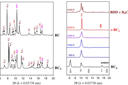
37 to 50 at%, the authors reached under HPHT phase segregation into boron carbide and boron-doped diamond (with about 1.8 at% of boron) or a mixture of diamond, boron carbide and boron, depending on the HPHT transformation parameters and the boron content of the starting material. For low carbon content (x between 1 and
4), above 20 GPa and between 2000 and 2500 K, a mixture of boron carbides (B4C
or B50C2) and cubic boron carbide phases (Figure I-11) is obtained. The amount of
cubic boron carbides formed increases with the temperature and with the carbon content of the precursor.
After compression at 24 GPa and heating at 2200 K in a diamond-anvil cell,
the XRD pattern of BC5 (Figure I-11) shows the formation of a c-BC5 phase, which is
the only crystalline phase contained in the sample. The presence of amorphous component has been ruled out by TEM and Raman spectroscopy. Therefore, the
totality of the precursor has been transformed into c-BC5, conserving the initial
composition BC5 (the composition has been confirmed by EELS). Such stoichiometry
means that boron-containing diamond has been obtained, with a boron content as high as 16 at%.
Concerning the nanostructure, the authors report from TEM that c-BC5 is
obtained as aggregates of 10-15 nm grains (though the TEM pictures are not presented in the original article). The material has been successfully obtained and quenched as a bulk using a large-volume press in the same pressure and
temperature conditions. Bulk samples showed a hardness of Hv = 71 GPa, which
places the material among the hardest known materials. The fracture toughness is
also very high at about 9.5 MPa.m0.5 (4.5 MPa.m0.5 for diamond). The material is
stable up to 1890 K, then transforms into graphite and amorphous boron or boron
carbide. All these results make nanostructured c-BC5 a very good candidate for
38
Figure I-11. Left: XRD patterns obtained after transformation of different BCx
precursors: a mixture of boron carbides B4C and B50C2, boron-doped diamond and c-BCx is
obtained. Right: In situ XRD patterns along compression and heating of t-BC5: compression
leads to loss of (00l) reflections. The pattern is not further modified until phase transition occurs at 1940 K. The cubic phase is synthesised at 2200 K. Further heating above 2440 K
leads to phase segregation into boron-doped diamond and boron carbide.32
Another nanostructured boron carbide has also been reported by Zinin et al.
who synthesised BC3 by laser-heating in a diamond anvil cell (DAC) from
turbostratic-like BC3 (t-BC3), containing a small amount of B4C (Figure I-12).33 At
44 GPa, a phase transition occurs at 1980 K reaching c-BC3. The chemical purity and
stoichiometry of c-BC3 are confirmed by EELS. However, c-BC3 synthesis was only
conducted in DAC, thus not reaching quantities allowing investigation of the mechanical properties.
Figure I-12. Left: XRD pattern of c-BC3. Right: HRTEM picture of c-BC3, evidencing its
nanostructure as 3-5 nm particles.33
Rubie et al. successfully synthesised a superhard material within the B-C-N
composition triangle.34 Indeed, at 28.5 GPa, turbostratic graphitic BC2N transformed
into a cubic phase above 2200 K. EELS studies conducted on that material
confirmed the composition, very close to BC2N.35,36 The synthesis was successfully