HAL Id: hal-01736090
https://hal.archives-ouvertes.fr/hal-01736090
Submitted on 8 Jun 2018HAL is a multi-disciplinary open access
archive for the deposit and dissemination of sci-entific research documents, whether they are pub-lished or not. The documents may come from teaching and research institutions in France or abroad, or from public or private research centers.
L’archive ouverte pluridisciplinaire HAL, est destinée au dépôt et à la diffusion de documents scientifiques de niveau recherche, publiés ou non, émanant des établissements d’enseignement et de recherche français ou étrangers, des laboratoires publics ou privés.
Fabrication of nanocrystal memories by ultra low energy
ion implantation
Nikolay Cherkashin, Caroline Bonafos, H. Coffin, Marzia Carrada, Sylvie
Schamm-Chardon, Gérard Benassayag, D. Chassaing, P. Dimitrakis, P.
Normand, M. Perego, et al.
To cite this version:
Nikolay Cherkashin, Caroline Bonafos, H. Coffin, Marzia Carrada, Sylvie Schamm-Chardon, et al.. Fabrication of nanocrystal memories by ultra low energy ion implantation. physica status solidi (c), Wiley, 2005, 2 (6), pp.1907–1911. �10.1002/pssc.200460523�. �hal-01736090�
Fabrication of nanocrystal memories by ultra low energy ion
implantation
N. Cherkashin*1,2 , C. Bonafos1 , H. Coffin1 , M. Carrada1 , S. Schamm1 , G. Ben Assayag1 , D. Chassaing1 , P. Dimitrakis3 , P. Normand3 , M. Perego4 , M. Fanciulli4 , T. Muller5 , K. H. Heinig5 , and A. Claverie1 1CEMES-CNRS, 29 rue J. Marvig, 31055, Toulouse, France
2
Ioffe Physico-Technical Institute, Polytekhnicheskaya 26, St Petersburg 194021, Russia
3
Institute of Microelectronics, NCSR 'Demokritos', 15310 Aghia Praskevi, Greece
4
Laboratorio MDM - INFM Agrate, Italy
5
Forschungszentrum Rossendorf, Institut für Ionenstrahlphysik und Materialforschung, PO Box 510119, 01314 Dresden, Germany
Received 11 September 2004, revised 8 October 2004, accepted 8 October 2004 Published online 7 April 2005
PACS 68.37.Lp, 81.07.Bc, 85.30.Pg, 85.35.Be, 85.40.Ry
In silicon nanocrystal based metal-oxide-semiconductor memory structures, tuning of the electron tunnel-ing distance between the Si substrate and Si nanocrystals located in the gate oxide is a crucial requirement for the pinpointing of optimal device architectures. In this work, we show how to manipulate and control the depth-position and the density of 2D arrays of Si ncs embedded in thin (<10 nm) SiO2 layers,
fabri-cated by ultra-low energy (typically 1 keV) ion implantation. It is demonstrated that the injection distance between the ncs band and the channel can be tuned from 10 to 2 nm by a judicious combination of ion beam energy and initial SiO2 thickness. Annealing under slightly oxidizing ambient has been found essen-tial for the optimization of the memory properties of the devices. During such oxidations, the oxide integ-rity is restored, the ncs are passivated and a separation of connected ncs takes place, making possible a further increase of the ncs density and a decrease of their mean size.
© 2005 WILEY-VCH Verlag GmbH & Co. KGaA, Weinheim
1 Introduction In silicon nanocrystal based metal-oxide-semiconductor (MOS) memory structures a
fine control of the Si nanocrystals (ncs) location in the gate oxide is required for the pinpointing of opti-mal device architectures [1]. The use of isolated Si clusters instead of continuous poly-Si layer decreases the overall coverage that weakens current leakage through underlying tunnel oxide by defect paths. It opens the promising way to continue scaling- down tunnel oxide and thus, to fabricate high-charge-density low-power-consuming devices. That is definitely required in such direct tunnelling regime is a fine control of the nanocrystal location since a change of less than 1 nm in tunnel oxide thickness dra-matically affects programming properties (write/erase times and voltages) and data retention [2, 3]. Among different deposition techniques [1, 4], like thermal oxidation of Si1–xGex [5] or ion implantation followed by annealing [6] used for the performance of nanocrystal memories, ultra-low energy Si im-plantation and subsequent thermal treatment has been recently demonstrated [7–9] to be the most attrac-tive one. But up to now no systematic studies of ncs formation processes have been performed. In this work, we show how to manipulate and control the depth-position and the density of 2D arrays of Si ncs embedded in thin (<10 nm) SiO2 layers, fabricated by ultra-low energy (typically 1 keV) ion implanta-tion. Specific experimental methods have been developed to characterize these populations of ncs. They
*
1908 N. Cherkashin et al.: Fabrication of nanocrystal memories by ultra low energy ion implantation
© 2005 WILEY-VCH Verlag GmbH & Co. KGaA, Weinheim
include Transmission Electron Microscopy (TEM) Fresnel imaging for the measurement of distances and widths of interest [9]; spatially resolved Electron Energy Loss Spectroscopy (EELS) using the spectrum-imaging mode of a Scanning Transmission Electron Microscope (STEM) to measure the size distribution and density of the ncs population and Time-of-Flight Secondary Ion Mass Spectroscopy (ToF-SIMS) to measure the depth-distribution of excess silicon in the oxide layer [11, 12]. The binary collision code TRIDYN [10] was used to predict the target stoechiometry after high-dose low-energy Si+ implantation into SiO2. It extends the commonly used TRIM program [13] to high-fluence implantation conditions and includes dynamic target changes, i. e. changes due to ion implantation, ion sputtering and ion beam mix-ing. We have used all these techniques to study the influence of implantation (energy, dose) and anneal-ing conditions (N2 or N2+1.5%O2 atmosphere) and oxide thickness on the characteristics of the ncs popu-lations and understand how they affect the charge storage properties of associated devices (capacitors and transistors). As a result of the carried out optimization both EEPROM-like and NVRAM-like transis-tors have been fabricated. Their characteristics will be discussed in relation with the characteristics of the 2D arrays of ncs on which they rely.
2 Experimental and simulation details Five sets of samples have been examined. All sample
de-tails are summarized in Table 1. Each set of samples is characterized by 4 parameters: nominal oxide thickness, energy, dose and annealing ambient. In Set 1 the energy was varying. In Set 2 SiO2 layers were implanted at the same energies than in Set 1, but the Si+
doses were chosen in such a manner that the peak concentration of the implanted Si reached always 35 at.% (in SiO2). These doses were predicted by TRIDYN [10]. Oxide thickness, dose and annealing atmosphere were varying parameters for respec-tively Set 3, 4 and 5. All the samples have been annealed at 950 °C. Specimens from all samples were prepared for both cross sectional TEM (XTEM) and plane-view observations using the standard proce-dure involving mechanical polishing and ion milling. A 60 nm thick poly-Si layer was deposited on top of the oxide to help in visualizing the SiO2 surface in XTEM images.
Table 1 Experimental conditions for five different sets of samples with the variation: of energy with fixed
dose(1) and peak excess (2) ; of nominal oxide thickness (3); of dose (4); of annealing ambient and time (5). Set of samples Nominal oxide
thickness (nm)
Energy (keV) Dose (cm–2) Annealing conditions Set 1 10 0.65, 1, 2, 3, 5 1016 950 °C 30 min , N2 Set 2 10 1 3 5 1016 2.1x10¹⁶ 3.2x10¹⁶ 950 °C 30 min, N2 Set 3 10 7 5 1 1016 950 °C 30 min, N2 Set 4 10 1 5x10¹⁵ 1016 2x10¹⁶ 950 °C 30 min, N2 Set 5 7 1 2x10¹⁶ 950 °C 30 min, N2 950 °C 30 min, N2+1.5%O2 950 °C 120 min, N2+1.5%O2
3 Results and discussion
3.1 Effect of the implantation energy and oxide thickness on the ncs position
For tuning the nanocrystal position within the SiO2 layer, our first attempt was to vary the implantation energy according to samples Set 1 of Table 1. As ion energy increases from 1 to 3 keV, the nanocrystal layer shifts deeper in the SiO2 layer, i.e., closer to the Si/SiO2 interface. Surprisingly, no ncs are detected
for 5 keV implantation, while HREM imaging (not shown) of the SiO2/Si interface reveals there unusual roughness.
Fig. 1 Series of XTEM images of samples Set 3, Table 1, taken under defocused bright field (Fresnel) conditions.
In order to compensate the decrease of the Si peak concentration with increasing ion energy, the experi-ment was repeated with ion doses adjusted to obtain a constant peak concentration of 35 at. % Si excess (samples Set 2 of Table 1). Again a nanocrystal layer is formed and shifts closer to the SiO2/Si interface at ion energies increasing from 1 to 3 keV. Moreover a rough interface is found at 3 keV and multiple twins and grains at 5keV.
Another way to decrease the injection distance is to keep fixed implantation conditions but to decrease the nominal oxide thickness. We have studied by TEM (see Fig. 1) the evolution of the characteristic distances for samples Set 3 of Table 1. While decreasing the oxide thickness 3 parameters remains con-stant: depth position of the ncs band with respect to the surface, its width and overall swelling of SiO2 layer. Thus for 5 nm oxide it is made possible to have an injection distance of 2 nm. ToF-SIMS meas-urements of these samples (see [14]) detect two regions of Si excess, i.e., the Gaussian like implantation profile and error-function-like profile at the interface due to ion mixing. These regions are well separated in the case of implantation at low energy (1 keV) even in 5 nm SiO2 layers. On the contrary, they overlap when increasing the implantation energy up to 5 keV. TRIDYN simulations combined with experimental data gives a safe explanation regarding the unique technological route of obtaining Si nanocrystals at distances smaller than 5 nm from the channel: the formation of nanocrystals requires that the interface mixing due to collisional damage does not overlap with the range profile to the extend that there is no more a local maximum of Si excess buried in the SiO2 layer.
3.2 Effect of the implanted dose The morphology of ncs layer strongly depends on the implanted
dose. The formation of Si ncs in 10 nm oxide by keeping the same implantation energy of 1keV but by varying the dose (5x10¹⁵
cm–2 , 1016
cm–2 , 2x10¹⁶
cm–2
) (samples Set 4 of Table 1) has been monitored through PEELS/STEM study (Fig. 2). Three main characteristics,- size, density, surface coverage- have been extracted from these images after their special software treatment. As it is well seen: 1) no ncs are detected at the lowest dose; 2) high dense array (3x10¹²
cm–2
) of sphere like ncs are formed at medium dose; 3) connected array of ncs with larger size and less density (1011
cm–2
) is created at highest dose.
Fig. 2 PEELS/STEM images of samples Set 4, Table 1 showing the effect of dose on Si ncs layer morphology: a)
5x1015 cm–2 ; b) 1016 cm–2 ; c) 2x1016 cm–2 . 10 nm 10 nm 7 nm 5 nm Poly-Si Si (a) (b) (c) 10 nm 10 nm 7 nm 5 nm Poly-Si Si (a) (b) (c)
1910 N. Cherkashin et al.: Fabrication of nanocrystal memories by ultra low energy ion implantation
© 2005 WILEY-VCH Verlag GmbH & Co. KGaA, Weinheim
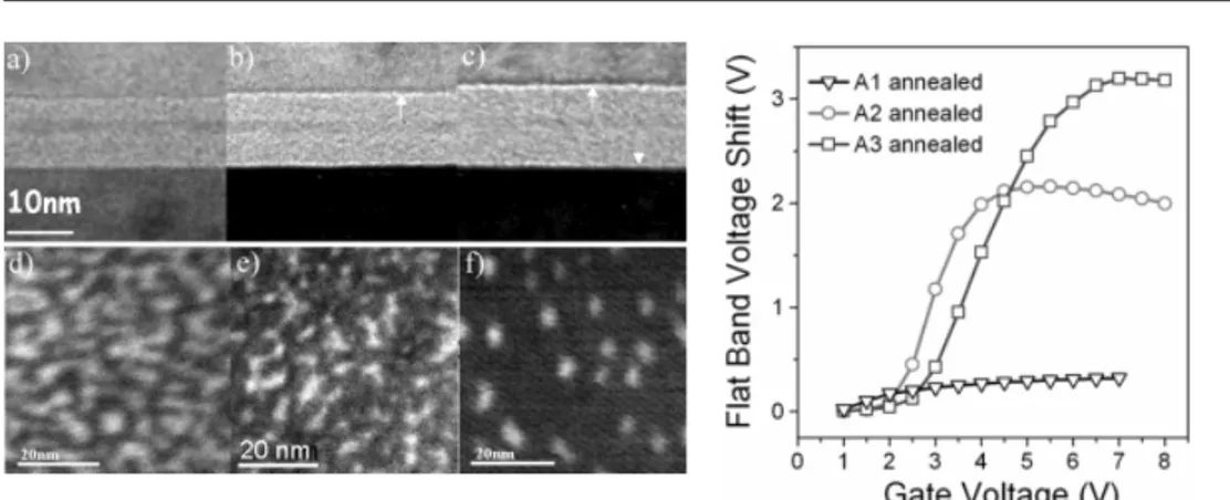
Fig. 3 XTEM (a,b, c) and PEELS/STEM (d, e, f) images
of samples Set 5, Table 1 showing the effect of anneal-ing ambient on Si ncs layer morphology: (a) and (d) 950 °C N2 30 min; (b) and (e) 950 °C 30 min, N2+1.5%O2; (c) and (f) 950 °C 120 min, N2+1.5%O2.
Fig. 4 Flat-band voltage shift (∆VFB) as a function of the
gate voltage round sweep for 7-nm-thick oxide layer implanted with 2x10¹⁶
Si/cm2
at 1 keV and subsequently annealed following the A1, A2, or A3 treatment.
The observed structural features as a function of dose are in rather good qualitative agreement with the ones predicted by kinetic 3D lattice Monte Carlo simulations [15]. Theses features are the nucleation and growth of sphere like and separated ncs at low Si+
fluencies but spinodal decomposition with creation of elongated and connected Si structures at higher fluencies. At the same time the values of doses needed to have ncs formed in experiment are twice higher then that in simulations. The reason for that is the partial loss of Si implanted dose during annealing as a result of O2 penetration through the damage induced by implantation [9].
3.3 Effect of the annealing ambient Apart from the damaged induced by implantation the integrity
of oxide is influenced by the presence of point defects inside. To restore the quality of the SiO2 layer it was proposed to use annealing in diluted oxygen environment [3] that should also have an impact on properties of ncs band. For this purpose we have studied the series of samples (Set 5 of Table 1) where after high dose low energy implantation annealing is applied at N2 atmosphere during 30 min and at (N2+1.5%O2) during 30 and 120 min. XTEM imaging (Fig. 3 a,b,c) reveals additional swelling of the control oxide after annealing in oxygen environment (Fig. 3 b,c). Moreover during longer annealing time (Fig. 3 c) such swelling is increased involving also injection oxide. As it is seen in PEELS/STEM images (Fig. 3 d) after annealing under N2 strongly connected coalesced elongated Si ncs are formed. By adding oxygen into annealing atmosphere the separation of coalesced ncs occurs (Fig. 3 e) [16]. After such long time annealing the system of well separated close to sphere like particles of highest density and less size is found (Fig. 3 f).
3.4 Electrical characterization The structural characterization that was described earlier allows to
make direct relation between morphology and ncs position with the electrical properties of capacitors and transistors based on Si ncs within gate oxide [17]. In particular, for studying the effect of oxidising ambient, samples with implantation conditions of Set 4 have been annealed under the following condi-tions: (A1) 950 °C, 30 min, N2; (A2) 950 °C, 15 min, N2+950 °C, 15 min, (N2+1.5%O2); (A3) 950 °C, 30 min, (N2+1.5%O2). The effect of A1, A2, and A3 post-implantation thermal treatments on the memory window is shown on Fig. 4. In comparison with A1 treatment, the magnitude of ∆VFB as a function of the gate voltage sweep strongly increases after A2 and A3 thermal treatments. It is believed that such an increase is due to the improved quality of the overall oxide, enhanced thickness of the control oxide and separation and passivation of Si initially connected ncs (see Fig. 3). This view is further supported as A2 and A3 treatments lead to oxides with a strongly reduced conductivity [3]. Both EEPROM-like and NVRAM-like transistors have been fabricated following this route depending on the distance of the ncs
layer to the electrodes. The memory window is detected at NVRAM like transistor with the application of symmetric +7 V/-7 V write/erase pulses of 1µs while at EEPROM-like transistor the gate voltage sweep is higher (+9 V/-9 V) and the programming time is longer (10 ms). The charge retention charac-teristics of the devices at room temperature shows that the flat band voltage window narrows down to 0.34 V after 11h of read delay time for NVRAM like transistor and down to 0.6 V (extrapolated value) after 10 years for EEPROM-like transistor respectively. These values are well comparable with already existing SONOS device characteristics that makes ncs based NVM even more attractive for future appli-cations due to their easier manufacturability integration.
4 Conclusions In this work, we show how to manipulate and control the characteristics of 2D arrays
of Si ncs embedded in thin SiO2 layers. The injection distance between the ncs band and the channel can be tuned from 8 to 2 nm by a judicious combination of ion beam energy and initial SiO2 thickness. An-nealing under slightly oxidizing ambient has been found essential for the optimization of the memory properties of the devices. During such oxidations, the oxide integrity is restored, the ncs are passivated and a separation of connected ncs takes place, making possible a further increase of the ncs density and a decrease of their mean size. We have demonstrated that EEPROM-like and NVRAM-like transistors fabricated following this route compete well with now existing SONOS structures.
Acknowledgements This work was partially supported by the European Commission through the Growth project
G5RD/2000/00320 – NEON (Nanoparticles for Electronics). The authors want to thank V. Soncini from ST Microe-lectronics Agrate for the oxidised wafers, A. Agarwal from Axcelis Technologies, Inc. for the implantation, M. Tencé and C. Colliex from LPS/Orsay for the PEELS/STEM images.
References
[1] S. Tiwari, F. Rana, H. I. Hanafi, A. Hartstein, E. F. Crabbé, and K. Chan, Appl. Phys. Lett. 68, 1377 (1996). [2] S. Tiwari, F. Rana, K. Chan, L. Shi, and H. Hanafi, Appl. Phys. Lett. 69, 1232 (1996).
[3] P. Normand, E. Kapetanakis, P. Dimitrakis, D. Tsoukalas, K. Beltsios, N. Cherkashin, C. Bonafos, H. Coffin, G. Benassayag, A. Claverie, V. Soncini, A. Argawal, and M. Ameen, Appl. Phys. Lett. 83, 168 (2003). [4] G. Ammendola, M. Vulpio, M. Bileci, N. Nastasi, C. Gerardi, G. Renna, I. Crupi, G. Nicotra, and S.
Lombar-do J. Vac. Sci. Technol. B 20, 2075 (2002).
[5] Y. C. King, T. J. King, and C. Hu, IEEE Trans. Electron Devices Meet. ED-48, 696 (2001).
[6] P. Normand, D.Tsoukalas, E. Kapetanakis, J. van den Berg, D. G. Armour, J. Stoemenos, and C. Vieu, Elec-trochem. and Solid State Lett. 88, 1 (1998).
[7] P. Normand, K. Beltsios, E. Kapetanakis, D. Tsoukalas, T. Travlos, J. Stoemenos, J. Van Den Berg, S. Zhang, C.Vieu, H. Launois, J. Gautier, F. Jourdan, and L. Palun, Nucl. Instrum. Methods Phys. Res. B 178, 74 (2001). [8] P. Dimitrakis, E. Kapetanakis, P. Normand, D. Skarlatos, D. Tsoukalas, K. Beltsios, V. Soncini, A. Claverie,
G. Benassayag, C. Bonafos, D. Chassaing, M. Carrada, and V. Soncini, Mater. Sci. Eng. B 101, 14 (2003). [9] M. Carrada, N. Cherkashin, C. Bonafos, G. Ben Assayag, D. Chassaing, P. Normand, D. Tsoukalas, V.
Son-cini, and A. Claverie, Mater. Sci. Eng. B 101, 204 (2003).
[10] W. Möller and W. Eckstein, Nucl. Instrum. Methods Phys. Res. B 2, 814 (1984).
[11] M. Perego, S. Ferrari, S. Spiga, E. Bonera, M. Fanciulli, and V. Soncini, Appl. Phys. Lett. 82, 121 (2003). [12] M. Perego, S. Ferrari, M. Fanciulli, G. Ben Assayag , C. Bonafos, M. Carrada, and A. Claverie, J. Appl.
Phys. 95, 257 (2004).
[13] J. P. Biersack and L. G. Haggmark, Nucl. Instrum. Meth. 174, 257 (1980). http://www.srim.org
[14] C. Bonafos, M. Carrada, N. Cherkashin, H. Coffin, D. Chassaing, G. Ben Assayag, and A. Claverie, J. Appl. Phys. 95 (10), 5696 (2004).
[15] T. Müller, C. Bonafos, K.-H. Heinig, M. Tencé, H. Coffin, N. Cherkashin, G. Ben Assayag, S. Schamm, G. Zanchi, C. Colliex, W. Möller, and A. Claverie, Appl. Phys. Lett. (in press).
[16] A. Wellner, V. Paillard, H. Coffin, N. Cherkashin, and C. Bonafos, Appl. Phys. Lett. 96, 2403 (2004). [17] P. Normand, E. Kapetanakis, P. Dimitrakis, D. Skarlatos, K. Beltsios, D. Tsoukalas, C. Bonafos, G. Ben