UNIVERSITÉ DE SHERBROOKE
Faculté de génie
PHOTOCORROSION DIGITALE DE MICROSTRUCTURES À
SEMI-CONDUCTEURS QUANTIQUES : UNE MÉTHODE DE
DIAGNOSTIQUE STRUCTURALE ET DE DÉTECTION DE
MOLÉCULES CHARGÉES ÉLECTRIQUEMENT
DIGITAL PHOTOCORROSION OF QUANTUM SEMICONDUCTOR
MICROSTRUCTURES: A METHOD FOR STRUCTURAL
DIAGNOSTICS AND SENSING OF ELECTRICALLY CHARGED
MOLECULES
Thèse de doctorat
Srivatsa AITHAL
Composition du jury :
Prof. Jan J. Dubowski, Université de Sherbrooke, directeur
Prof. Mohamed Chaker, Institute National de la Recherche
Scientifique, expert externe
Prof. Eric H. Frost, Université de Sherbrooke, expert interne
Prof. Serge Charlebois, Université de Sherbrooke, rapporteur
La fabrication de dispositifs à base de structures multicouches de semi-conducteurs exige une mesure de routine des épaisseurs et de la localisation des interfaces des couches formées. Ceci est souvent réalisé en utilisant des techniques coûteuses et compliquées telles que la microscopie à force atomique (AFM) ou la spectroscopie de photoélectrons à rayons X (XPS). Dans ce travail, la métrologie à température ambiante dans un environnement aqueux a été développée pour des tests de post-croissance des nano-hétérostructures (NHs) semi-conductrices. La méthode utilise le procédé de photocorrosion numérique (DIP) et la sensibilité de l'émission de photoluminescence (PL) aux états de surface révélés pendant la photocorrosion.
Le processus de photocorrosion des NHs semi-conducteurs GaAs/AlGaAs a été étudié en présence d'une excitation la bande interdite d'échantillons immergés dans différentes solutions aqueuses. Une photo-excitation de faible intensité au-dessus de la bande interdite (<105 mW/cm2) a été
appliquée en mode pulsé caractérisée par un duty cycle (DC) donné par TON/(TON + TOFF). Ceci a
produit des vitesses moyennes de gravure du matériau enleves à la précision de la sous-monocouche pendant chaque cycle DIP. En utilisant les techniques d’AFM et de XPS, il a été démontré que l'émission de la PL d'une NH GaAs/AlGaAs au cours de la DIP oscille en raison des couches de GaAs et d’AlGaAs révélées. Ces oscillations sont causées par la sensibilité de l'émission PL à la vitesse de recombinaison de surface des porteurs, qui diffère considérablement pour GaAs et AlGaAs. Le processus DIP a révélé une épaisseur de 1 nm de GaAs dans une structure de GaAs/AlGaAs, mais cela ne semble pas être une limite de résolution de cette approche.
Le potentiel de circuit ouvert (OCP) mesuré au cours du DIP diffère entre les jonctions d'électrolyte-GaAs et électrolyte-AlGaAs formées au cours du processus de la photocorrosion. Les différences de OCP sont interprétées comme pouvant provenir des photo-oxydes superficiels qui portent la charge électrique. Le dipôle formé par ces oxydes superficiels définit l'OCP mesuré. L'oscillation de l’OCP pourrait également être utilisée pour la métrologie des NHs. Cela ouvre la perspective d'étendre la métrologie DIP aux NHs semi-conducteurs avec un signal PL non existant ou négligeable.
Enfin, les entités chargées proches du voisinage d'une surface semi-conductrice affectent le taux de DIP. Cette propriété a été utilisée pour détecter la Legionella pneumophila qui est normalement chargée négativement au pH> 4. Les mesures de FTIR ont indiqué que les monocouches auto-assemblées (SAM) d’alkanethiol restent sur la surface semi-conductrice pendant le DIP. Cela a permis la détection de la Legionella pneumophila vivante à une concentration de 105 CFU/mL avec une architecture simple à base d'anticorps. Une discussion a
été proposée suggérant des protocoles de biocapteurs possibles pour atteindre des limites de détection améliorées avec le biocapteur DIP.
Mots clés : Photoluminescence; Potentiel de circuit ouvert; Photocorrosion numérique; Les
microstructures GaAs/AlGaAs; La métrologie des nano-hétérostructures; Biocapteur; Legionella pneumophila;
Fabrication of devices based on semiconductor multilayer structures demands routine measurement of thicknesses and location of the interfaces of the constituent layers. This is often achieved using expensive and complicated techniques such as scanning electron microscopy, secondary ion mass spectroscopy, atomic force microscopy (AFM) or x-ray photoelectron spectroscopy (XPS). In this work, room temperature metrology in water environment has been developed for post-growth testing of semiconductor nanoheterostructures (NHs). The method utilizes the process of digital photocorrosion (DIP) and the sensitivity of photoluminescence (PL) emission to surface states revealed during photocorrosion.
The photocorrosion process of GaAs/AlGaAs semiconductor NHs has been investigated in the presence of above bandgap excitation of samples immersed in different aqueous solutions. In order to achieve precise control over photocorrosion rates, the NH samples were placed in a flow cell with controlled aqueous environment. A low intensity above-bandgap photoexcitation (< 105 mW/cm2) was incident in a pulse mode and characterized by a duty cycle (DC) given by
TON/(TON + TOFF). This has produced average etch rates of material removed at sub-monolayer
precision during each DIP cycle. Using AFM and XPS, it has been demonstrated that the PL emission from a GaAs/AlGaAs NH during DIP oscillates owing to revealed GaAs and AlGaAs layers. These oscillations are caused by the sensitivity of the PL emission to the carrier surface recombination velocity, which drastically differs for GaAs and AlGaAs. The DIP process has revealed a 1 nm thick GaAs in a GaAs/AlGaAs NH structure, but this does not seem to be the resolution limit of this approach.
Open circuit potential (OCP) measured during DIP differs amongst GaAs-electrolyte and AlGaAs-electrolyte junctions formed during the photocorrosion process. The OCP oscillations were found in-phase with the PL oscillations measured during DIP. The differences of OCP are theorized to originate from the surficial photo-oxides that carry electric charge. The dipole formed by these surficial oxides define the measured OCP. The OCP oscillation could also be used for metrology of NHs. This opens the prospect of extending the DIP metrology to semiconductor NHs with non-existing or negligible PL signal.
Lastly, charged entities near the vicinity of a semiconductor surface affects the rate of DIP. This property has been utilized to detect Legionella pneumophila that normally are negatively charged at pH > 4. Fourier transform infrared spectroscopy measurements have indicated that alkanethiol self-assembled monolayers (SAMs) remain on the semiconductor surface during DIP. This has allowed for the detection of live Legionella pneumophila at 105 CFU/mL with a simple
antibody-based architecture. A discussion has been provided suggesting possible biosensing protocols for achieving enhanced detection limits with the DIP biosensor.
Key words: Photoluminescence; Open circuit potential; Digital photocorrosion; GaAs/AlGaAs
I would like to sincerely thank my advisor Prof. Jan J. Dubowski for the invaluable guidance, financial and technical support during my PhD. Dr. Eric H. Frost has been important to my growth as a researcher, I thank and appreciate his support.
I greatly value and appreciate the time and effort taken by my committee members, Prof. Eric H. Frost, Prof. Serge Charlebois, and Prof. Mohamed Chaker to help improve my work.
I wish to thank Dr. Khalid Moumanis and Dr. Walid Hassen for all the support both inside and outside the lab.
This work would not be possible without the camaraderie, support and help from current and former members of QS group, Neng Liu, Mohammed Reza Aziziyan, Lilian Sirbu, Hemant Sharma, Xiaohuan Huang, Dominic Carrier and Elnaz Nazemi.
Finally, none of this work would be possible without the support of my late father, mother, bother and my long-suffering partner Dr. Nosrati. I cannot thank them enough.
1 INTRODUCTION ... 16
2 STRUCTURAL DIAGNOSTICS OF SEMICONDUCTOR SURFACES AND HETEROSTRUCTURES ... 19
2.1 Conventional methods ... 19
2.2 Photocorrosion of GaAs ... 21
2.3 Photoetching of semiconductor heterostructures ... 21
3 SENSING OF ELECTRICALLY CHARGED MOLECULES IN WATER ... 23
3.1 Biosensing ... 23
3.2 Biosensing receptors ... 24
3.3 Biosensing Transducer ... 25
4 GOALS OF THIS WORK ... 29
5 EXPERIMENTAL METHODS AND TOOLS ... 30
5.1 Semiconductor samples ... 30
5.2 Photoluminescence ... 32
5.2.1 Basic principle ... 32
5.2.2 Photocorrosion setup... 34
5.2.3 Detection of electrically charged molecules using DIP ... 37
5.3 Biofunctionalization ... 38
5.3.1 Sample surface preparation ... 38
5.3.2 SAMs formation on GaAs ... 38
5.3.3 Antibody conjugation ... 39
5.4 X-ray photoelectron spectroscopy ... 40
5.5 Fourier transform infrared spectroscopy ... 41
6 RESULTS AND DISCUSSION... 43
6.1 Foreword: Article 1, Photocorrosion metrology of photoluminescence emitting GaAs/AlGaAs heterostructures ... 43
6.2 Foreword: Article 2, Open circuit potential monitored digital photocorrosion of GaAs/AlGaAs quantum well microstructures ... 64
6.3 Digital photocorrosion based biosensing ... 76
6.3.1 Stability of SAM during photocorrosion ... 76
6.3.2 Reproducibility of the thiolation process ... 78
6.3.3 Surface coverage of bacterial binding: Fluorescent microscopy study ... 79
6.3.4 Photocorrosion based sensing of live Legionella pneumophila ... 80
Fig. 1. (a) Cyclic voltammetry of GaAs and AlGaAs in dark and irradiated with halogen lamp of 95 mW/cm2 continuous photoexcitation intensity. (b) Temporal current density during photoelectrical etching of
AlGaAs/GaAs heterostructure (Fink & Osgood, 1993). ... 22
Fig. 2. Prototypical biosensing processes ... 24
Fig. 3 Schematic of structures of various classes of antibodies (https://bxcell.com/antibody-structure/) 25 Fig. 4 Schematic of the investigated heterostructures used in this work and their corresponding PL emission spectra. Wafer 10-150 (a), v0803 (e), and AXT14-287 (i) have their PL emission maxima at 869 nm. Wafer 10-413 (c) is a QW microstructure that emits at 829 nm (d). Wafer JD2C (g) a QW microstructure with emission at 850 nm (h). ... 32
Fig. 5 Energy (E) – momentum (k) diagram showing absorption of photon in a direct bandgap and indirect bandgap semiconductor (Van De Krol, 2012). In this figure, ω is the frequency of a phonon, k is the momentum and ν the frequency of the photon. ... 33
Fig. 6. PL spectra for GaAs coated with various oxides using molecular beam epitaxy (Passlack et al., 1996). ... 34
Fig. 7. Fluidic system block diagram ... 35
Fig. 8 A schematic view of the QSPB and flow cell setup. ... 36
Fig. 9 Time dependent PL emission (at 869 nm) of a GaAs/AlGaAs NH (sample AXT14-287) immersed in NH4OH and irradiated in QSPB with a 660 nm LED at DC = 1 s/100 s (a), and a plot of the position of PL maxima vs. cumulative thickness of the NH (b). ... 37
Fig. 10 PL peak position vs. different concentrations of E. coli K 12 bacteria (Nazemi et al., 2015). ... 38
Fig. 11 Functionalization of GaAs with PEG-Biotin, antibody and bacterial binding. ... 39
Fig. 12 Schematic of XPS measurement setup (a) and energetics of the XPS process (b). ... 40
Fig. 13 FTIR setup in the transmission mode. ... 41
Fig. 14 FTIR spectra of SAM on GaAs corresponding to symmetric and asymmetric vibrations of CH2 (Huang, Liu, Moumanis, & Dubowski, 2013). ... 42
Fig. 15 Temporal PL reponse of MHDA SAM coated 10-413 sample digitally photocorroding in DI water. The arrows indicate approximate positions of the GaAs/AlGaAs interfaces. ... 76
Fig. 16 Transmission FTIR spectra of 10-413 MHDA SAMs formed in ethanol before DPC(a), post DPC in DI water (b) and after deoxidation with NH4OH (c). ... 77
Fig. 17 Transmission FTIR spectra of 10-413 MHDA SAMs formed in ethanol for four samples; sample 1 (S1), sample 2 (S2), sample 3 (S3) and sample 4 (S4). ... 78
Fig. 18 Illustration of the scheme to fluorescently tag immobilized bacteria. ... 79
Fig. 19 Representative temporal PL curves for biochip functionalized with Legionella antibody exposed to freshly prepared live Legionella pneumophila at 106 and 105 CFU/mL, and to PBS solution. ... 81
Table 1 Parameters measured, techniques used and references for characterization of semiconductors. ... 19 Table 2 Sensors and transduction mechanisms ... 26 Table 3 Detection limits and time for analysis for different methods of detecting Legionella pneumophila. ... 28 Table 4 Solution concentration of L. pneumophila and surficial density of immobilization studied by fluorescent antibody staining. ... 80 Table 5 PL maxima positions for live Legionella pneumophila detection runs (n represents replicates). .. 81
BCE Bacteria capture efficiency CRP C reactive protein
CFU Colony forming units DE Digital etching
DI Deionized
DIP Digital photocorrosion DNA Deoxyribonucleic acid ECL Electro-chemiluminescence
EDC 1-Ethyl-3-(3-dimethylaminopropyl)-carbodiimide FRET Förster resonant energy transfer
FITC Fluorescein 5(6)-isothiocyanate HRP Horse radish peroxidase
HI-PLM Hyper-spectral imaging mapper HUS Hemolytic uremic syndrome IgG Immunoglobulin G
IPA Isopropanol
LED Light emitting diode LOD Limit of detection
MHDA Mercapto hexadecenoic acid NHs Nano-heterostructure NHS N-hydroxy sulfo succinimide pI Isoelectric point
PEG-B Poly ethylene glycol thiol - Biotin PSA Prostate specific antigen
QSPB Quantum semiconductor photonic biosensor
QSPBN Quantum semiconductor and photon-based bionanotechnology RNA Ribonucleic acid
SAM Self-assembled monolayer
SELEX Systematic evolution of ligands by exponential enrichment SERS Surface-enhanced Raman spectroscopy
SPW Surface plasma wave
SQUID Superconducting quantum interference device TTP Thrombotic thrombocytopenic purpura
1 INTRODUCTION
This thesis is focused on investigation of a so-called digital photocorrosion (DIP) effect in GaAs/AlGaAs nano-heterostructures (NHs), and exploring its application for a) post epitaxial growth diagnostics, and b) detection of electrically charged molecules immobilized in the vicinity of such NH. The work describes the fundamental parameters of the DIP process and it demonstrates the potential of DIP in providing attractive information about structural parameters of semiconductor NH. The results of this work also clarify on some of the fundamental aspects concerning the quantum semiconductor photonic biosensing (QSPB) technology investigated by the Université de Sherbrooke Quantum Semiconductors (QS) Group.
Semiconductor devices based on multiple layers of thin semiconductors are ubiquitously used in consumer, defense and medical applications. Applications that require operation in radio frequencies such as cellphones, WiFi routers and solar cells for space applications use this multilayer semiconductor technology (Bhattacharya, Fornari, & Kamimura, 2011a; Dimroth et al., 2014; E Pettenpaul, 1998). Consistent and reproducible fabrication of multi-layer devices are affected by variation in thickness of layers, roughness at the interfaces, variation in carrier recombination rates and Schottky barrier height. Post-growth metrological tools are normally used to measure these parameters (Schroder, 2006). Etching is one of the critically important processes during fabrication of multilayer devices. This process usually involves removal of a material from photoresist patterned substrates. Since conventional plasma etching and wet etching techniques leave microscopically damaged surfaces, there has been an urgent need of developing alternative methods of nanostructuring of materials. One of the most advanced methods responding to this need is digital etching (DE) that allows processing of semiconducting materials with repeated, self-terminating cycles involving a gas phase reactants (Meguro & Aoyagi, 1997) or wet etching of the products of surface localized reactions (DeSalvo et al., 1996). In DE, etchant gas pulses and Ar ions are sequentially impinged onto the substrate surface to be etched. For GaAs, a typical etchant gas pulse is Cl2 and the 0.5 monolayers or 0.142 nm of GaAs is
removed in each cycle (Takashi et al., 1990). Due to lack of in situ monitoring techniques, these numbers are based on post-processing measurements. The application of the DIP process for etching of semiconductor NHs allows monitoring in situ position of the photocorrosion front with a sub-monolayer precision(Nazemi, Aithal, Hassen, Frost, & Dubowski, 2015). The investigation of fundamental parameters affecting DIP and application of this process for post-growth metrology of quantum well (QW) microstructures and selected NH represent the 1st axis of the research
undertaken in the frame of this project.
The 2nd axis of the undertaken research concerns the investigation of the DIP process for
detection of electrically charged molecules. Biomolecules are characterized by a pH and salt dependent electrical charge due to their constituent ionizable groups (Salgin, Salgin, & Bahadir, 2012; Salis et al., 2011). For example, Bovine serum albumin (BSA) has an overall negative charge of 18 electrons at pH 7 (Fologea, Ledden, McNabb, & Li, 2007). Isoelectric point (pI), the pH at which there is zero net charge, of many viruses lie between 3.5 < pI < 7 (Michen & Graule, 2010). A vast majority of bacteria are negatively charged at pH 7 (A. T. Poortinga, Bos, Norde, & Busscher,
2002). Rapid detection of viruses, bacteria and other pathogenic biomolecules, including the assessment of the interaction between such biomolecules and living organisms are of a great interest to the modern life science sector that, despite of a tremendous progress demonstrated since the invention of the electrochemical biosensor in 1962 (Clark & Lyons, 1962) still suffers from the lack of an inexpensive, rapid and precise quantification method of biological entities. Biosensing is the science of recognition and quantification of an analyte, which includes unicellular organisms like bacteria and amoeba, virus, protein, DNA, RNA, or biologically relevant organic and inorganic molecules, hereafter referred to as analyte. Prototypical analytes for human diagnosis and prognosis include biomarkers such as, c-reactive protein (CRP), prostate-specific antigen (PSA) for prostate cancer and, troponin T and troponin I for cardiac events (Hamm et al., 1997).
Bacteria are unicellular microorganisms without a nucleus. Bacteria in the human body outnumber human cells by a factor of 10. Bacterial flora in human gut have increasing found to influence human health (Lynch & Pedersen, 2016). Many species of naturally occurring bacteria and other microorganisms are pathogenic, i.e. they induce disease in humans.
Among the conventional methods, the gold standard for routine detection of bacteria is culture, which in microbiology refers to the transfer of an organism from its ecological niche (e.g., water stream), transient vehicle (e.g., food), or storage medium (as in case of stock culture), into a growth-permitting laboratory medium. The inoculated medium is then incubated, under optimum growth conditions and for a suitable length of time, to allow cell multiplication, resulting in a culture of the organism (Zourob, Elwary, & Turner, 2008). In practice, a majority of the bacteria are not-culturable using standard methods (Vartoukian, Palmer, & Wade, 2010).
Environmental monitoring of microorganisms for drinking water require monitoring Cryptosporidium, Giardia lamblia, Legionella and E. coli among others. In many cases, 80% of the costs involved with hazardous place cleanup are for lab tests, for sampling and monitoring, microorganisms (Ho, Robinson, Miller, & Davis, 2005). Legionella pneumophila occurs at low levels in natural sources of water and soil. They multiplie in warm water conditions such as in cooling towers, evaporation condensers, humidifiers, warm water tanks and other water reservoirs. L. pneumophila typically forms biofilms, which provide a habitat and gradient for nutrients (Murga et al., 2001). Additionally, increased occurrence of L. pneumophila infected amoebae compared to natural sources have also been observed in the case of water from cooling towers (Berk et al., 2006). L. pneumophila is responsible for Legionnaire’s disease, severe pneumonia and non-pneumonic Pontiac fever syndrome. The common methods for detection of
Legionella in the environment include PCR and culture that is considered the “gold” standard for
detection of bacteria, but due to the slow growing nature of Legionella (Stølhaug & Bergh, 2006), other methods are necessary. Bacterial biosensors often target the whole cell, DNA and RNA. Nucleic acid sensing requires a sample isolation and purification step. Whole cell sensors often face the challenge of bringing the bacteria to interact with the sensor surface. Techniques such as dielectrophoresis and chemotaxis are often used to overcome the whole cell transport limitation. (Burlage & Tillmann, 2017; W. Hassen et al., 2016). This activity represents a large effort of the QS Group towards rapid and automated detection of bacteria, such as Escherichia
coli and Legionella pneumophila bacteria that, under normal conditions (pH > 5), are
characterized by a relatively strong negatively charged outer shell (Soni, Balasubramanian, Beskok, & Pillai, 2008).
2 STRUCTURAL DIAGNOSTICS OF SEMICONDUCTOR
SURFACES AND HETEROSTRUCTURES
2.1 Conventional methods
Heterojunction semiconductor devices based on multilayer sandwiched of semiconductors find wide application in consumer electronics and photonics. Heterojunction bipolar transistors and high electron mobility transistors (Bhattacharya, Fornari, & Kamimura, 2011b) form the core technology enablers for RF components in ubiquitous devices such as mass-produced cellphones, satellite communication devices and car radars (E. Pettenpaul, 1998). High efficiency heterojunction solar cells used in concentrated photovoltaics (Dimroth et al., 2014) are examples of devices taking advantage of the semiconductor multilayer technology.
These devices are manufactured using photolithography, which involves deposition, patterning and etching of semiconducting materials. The successful fabrication of such devices depends on the quality of semiconductor wafers that relies on advanced diagnostic and metrology tools frequently employed as post-growth interrogation about such parameters as layer thickness, interfacial roughness, material composition, density of carriers and interface traps, or Schottky barrier height (Schroder, 2006). One or more of these parameters are critical for appropriate functioning of such devices. The most common methods employed for characterization of physical and chemical properties of semiconductor are summarized in table 1.
Table 1 Parameters measured, techniques used and references for characterization of semiconductors.
Property Measured Techniques References
Crystal quality X-ray diffraction, transmission electron microscopy, scanning electron microscopy
(Gerardi, Giannini, Passaseo, & Tapfer, 1997; Nakashima & Tateno, 2004) Interfacial roughness Atomic Force Microscopy (Oliver,
2008)
Composition
Secondary ion mass spectroscopy, x-ray photoelectron spectroscopy, Auger
electron spectroscopy (Gerardi et al., 1997; Herrmann, Lehnhardt, Strauß, Kamp, &
Forchel, 2011; Liu &
Dubowski, 2013)
Layer thicknesses
Scanning electron microscopy, transmission electron microscopy,
reflectance spectroscopy, (Linkov, Artemyev, Efimov, & Nabiev, 2013; Wośko et al., 2011)
Band structure, carrier concentration
Current-voltage (I-V), capacitance-voltage (C-V) measurements, photo-electrochemical profiling (Blood, 1986; Fleetwood et al., 1993; Kaniewska & Slomka, 2001)
Band offsets Photo-voltage spectroscopy
(Kronik & Shapira, 2001; Masut, Roth, Dubowski, & Lenchyshyn, 1986) Surface defects Electrochemical imaging
(Simpson & Rodríguez-López, 2015)
The thickness of semiconductor layers constituting heterostructure devices is one of the fundamental parameters determining functional characteristics of (QW) and other quantum confined microstructure based devices. Typical methods for determining this parameter are based on cross-section SEM or TEM imaging (Perovic et al., 1995), ellipsometric analysis (Erman, Theeten, Vodjdani, & Demay, 1983), depth profiling with Auger electron spectroscopy (J. J. Dubowski, D. F. Williams, P. B. Sewell, & Norman, 1985), SIMS (Liu, Poulin, & Dubowski, 2013) and x-ray diffraction techniques (Tapfer & Ploog, 1986). In situ monitoring the growth process of NH could be carried out with reflection high-energy electron diffraction technique (e.g., (Franke, Kreutzer, Zacher, Naumann, & Anton, 1998)), but no such diagnostics is available for in situ monitoring of material etched with a comparable (sub-monolayer) resolution.
Location of interfaces of QWs and quantum dots could be profiled using photo-electrochemical techniques. Owing to the small dimension of these devices, method with high etch rates cannot be readily applied in such applications (Fink & Osgood, 1993). For example, laser-induced
photoetch rates for GaAs and InP are in the range of 0.1 – 100 µm/min (Ruberto et al., 1991). Moreover, high surface roughness of the photoetched surface, over 15 nm (Kirchner et al., 2002), also limit ready application of photo-electrochemical techniques to these methods.
2.2 Photocorrosion of GaAs
Photocorrosion of bulk GaAs has been reported in literature as a “photowashing effect” (Ruberto et al., 1991). Upon photoexcitation, GaAs in contact with an electrolyte undergoes oxidation and photo-decomposition of n-type GaAs could be described by the following reactions:
𝑮𝒂𝑨𝒔 + 𝟓𝑯𝟐𝑶 + 𝟔𝒉+ → 𝑮𝒂𝟑++ 𝑯𝑨𝒔𝑶
𝟐+ 𝟑𝑯+ Reaction 1
𝑮𝒂𝑨𝒔 + 𝟑𝒆 → 𝑮𝒂𝟎+ 𝑨𝒔 Reaction 2
where h+ represents the holes in the semiconductor and H+ is the proton in the solution, e
represents the electron and Ga0 denotes a reduced gallium atom. The water environment and
excited holes arriving at the semiconductor surface lead to oxidation, and the reactions represented by equations (1) and (2) describe oxidation and dissolution of GaAs upon photo-excitation. The built-in potential at the liquid-solid junction drives the current that is responsible for the photocorrosion process. Application of bias to the semiconductor, presence of redox species in the liquid phase, pH of the solution, wavelength of incident light, dynamics of dissolution of corrosion products and presence of charged or ionizable species at the semiconductor-electrolyte junction affect the photocorrosion process.
2.3 Photoetching of semiconductor heterostructures
Application of photocorrosion as a wet etching process for AlGaAs/GaAs multilayer structures has been investigated by Fink and Osgood (Fink & Osgood, 1993). Photocorrosion was performed on MBE grown n-Al0.3Ga0.7As/n-GaAs in dilute nitric acid (HNO3:H2O = 1:20). The cyclic voltammetry
curves (CV) for GaAs and AlGaAs, and temporal current density in constant current mode are given in figure 1.
Fig. 1. (a) Cyclic voltammetry of GaAs and AlGaAs in dark and irradiated with halogen lamp of 95 mW/cm2 continuous photoexcitation intensity. (b) Temporal current density during
photoelectrical etching of AlGaAs/GaAs heterostructure (Fink & Osgood, 1993).
CV curves without photoexcitation for both GaAs and AlGaAs behave the same way and are indicated as “Dark Etching” in figure 1(a). The onset of anodic reaction starts after an overvoltage of +0.5 V and essentially follows Eq. 1 and, while hydrogen evolution starts at about -0.5 V. With photoexcitation, the photogenerated carriers induce a current in the CV response of GaAs and AlGaAs within the -0.5 V to 0.5V window. Thus, only the illuminated portions of the sample were photocorroded. Energy band diagram, near the semiconductor-electrolyte interface, is shown in figure 3(b). The conduction and the valence bands are bent upwards and holes to accumulate at the surface of the heterostructure. At points ‘A’, ’B’ and ‘C’ indicated in the temporal current density plot, the variation in the current density could be attributed to the peculiarities of the band structure variations during etching. At points ‘A’ and ‘C’, photogenerated carriers are present in AlGaAs or GaAs, respectively, and there are no additional potential barriers for the holes to reach the semiconductor surface. Whereas at point ‘B’, photogenerated carriers appear both in GaAs and AlGaAs. The holes in GaAs experience a potential barrier formed by AlGaAs. The etch rate in this case, R (nm/min), has been relatively slow and followed the relation 𝑅 = 15 × 𝑐𝑢𝑟𝑟𝑒𝑛𝑡 𝑑𝑒𝑛𝑠𝑖𝑡𝑦(𝑚𝐴/cm2) dependence for both GaAs and AlGaAs layers.
Photocorrosion effect of PL emitting GaAs/AlGaAs heterostructures employed for monitoring biomolecular binding involving electrically charged molecules that allowed for a rapid detection of bacteria in aqueous solutions has been demonstrated recently (Aziziyan, Hassen, Morris, Frost, & Dubowski, 2016; Nazemi et al., 2015). This was possible thanks to creating conditions for uniform photocorrosion proceeding at typically under ~60 nm/min, which represent etch rates on the order of one monolayers for each cycle of photoexcitation. In the current work, we investigate the mechanisms of GaAs and AlGaAs photocorrosion in water and aqueous environment of NH4OH, and we examine the conditions leading to the high-sensitive resolution
3 SENSING
OF
ELECTRICALLY
CHARGED
MOLECULES IN WATER
Biomolecules and biological entities such as lipids, proteins, carbohydrates, nucleic acids, virus, bacteria, cells, etc., are normally electrically charged (Salgin et al., 2012; Zhang et al., 2008). Charge and electrostatic interactions determine the structure, stability, binding affinity, chemical properties, and biological reactivity of proteins (Akke & Forsén, 2004; Chu et al., 2012; Sharp, 2002). Bacterial cell surfaces possess net negative electrostatic charge by virtue of ionized phosphoryl and carboxylate substituents on outer cell envelope of such macromolecules exposed to the extracellular environment (Wilson, Wade, Holman, & Champlin, 2001). This charge property of biomolecules has been used in conjunction with electric field-effect transistor based sensors for detection of DNA hybridization (Fritz, Cooper, Gaudet, Sorger, & Manalis, 2002) and antibody-antigen reaction in an immuno-field effect transistor (Immuno-FET) for Carcinoembryonic antigen, a cancer marker, has been developed using the AlGaN/GaN-based high-electron mobility transistor (HEMT) technology (Sarangadharan, Chu, Hsu, & Wang, 2015).
As discussed in section 1, biomolecules are charged at pH away from their isoelectric point (pI). Hence, biomolecular adsorption in the vicinity of a semiconductor can perturb the electrostatics of the semiconductor surface. This will typically result in the change of the built-in electric field in the proximity of the semiconductor surface, leading to the modulation of the surficial hole concentration and, consequently, perturbing the speed of the photocorrosion (Ruberto et al., 1991). The second channel of modulation of semiconductor surface properties is through charge transfer. It has been suggested that a charged entity such as bacteria could transfer some charge during adhesion to a semiconductor surface (A. Poortinga, Bos, & Busscher, 1999). These authors have claimed that E. coli adhering onto the indium tin oxide surface could be characterized with a charge totaling 10-14 C per bacterium, i.e., ~ 105 electrons per bacterium.
Transfer of the charge could also result in perturbation of the electric field near the semiconductor surface, thus affecting the photocorrosion process.
3.1 Biosensing
The International Union of Pure and Applied Chemistry (IUPAC) defines biosensor as a device that uses specific biochemical reactions mediated by isolated enzymes, immunosystems, tissues, organelles or whole cells to detect chemical compounds usually by electrical, thermal or optical signals (Nagel, Dellweg, & Gierasch, 1992). Biosensing process typically consists of two separate but related processes, recognition and transduction as illustrated in figure 2. Recognition is the selective affinity of the receptor to the analyte of interest, and transduction refers to conversion of this binding into an electrical or optical signal. Recognition is typically performed by naturally occurring receptor to the target of interest.
Fig. 2. Prototypical biosensing processes
3.2 Biosensing receptors
Receptors are chosen by their selective affinity to the analyte of interest. Common receptor analyte interactions include, nucleic acid interaction between complementary strands of DNA (hybridization) (Wang, 2002), antibody antigen interaction (Rowe, Scruggs, Feldstein, Golden, & Ligler, 1999) and, nucleic acid ligand interactions in aptamers (Subramanian et al., 2013).
Nucleic acids are central molecules in transmission, expression, and conservation of genetic information (Bloomfield & Crothers, 2000). They are present in all known forms of life. Two forms of nucleic acids are deoxyribonucleic acid (DNA) and ribonucleic acid (RNA), these two are known to carry information and allow for transcription of proteins. Nucleic acids have differential affinity to ligands such as small molecules, proteins, nucleic acids and cells. Repeated in vitro selection (SELEX - systematic evolution of ligands by exponential enrichment) allows for isolation of sequences with high affinity to the ligand of interest.
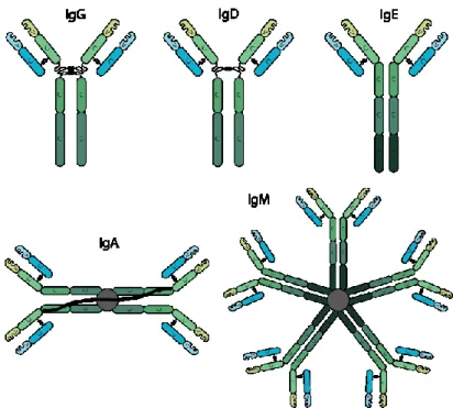
Antibodies are proteins produced by the immune system with the primary function of recognizing foreign targets. There are five classes of antibodies IgG, IgM, IgA, IgD and IgE, each of these have different structure, molecular weight and number of “binding sites”. Their foreign targets include proteins, small molecules and bacteria. An antibody can be divided into two distinct regions, variable and constant regions as shown in figure 3.
T
ra
n
sduc
er
Recognition element AnalyteFig. 3 Schematic of structures of various classes of antibodies (Bxcell, 2018)
The variations in the amino acids present in the variable region, which are antigen specific differ from one antibody to another. Lock and key hypothesis is generally accepted (Notkins, 2004) to explain the binding between antibody and antigen. In practice antibodies are manufactured as monoclonal, polyclonal or recombinant antibodies. Monoclonal antibodies are grown by B cells that have been fused with myeloma cells, whereas polyclonal antibodies are produced by immune reaction of an organism containing multiple immune cells which can recognize a plurality of epitopes, which are subsequently purified (Byrne, Stack, Gilmartin, & O’Kennedy, 2009). Recombinant antibodies are produced by genetic engineering, this allows antibodies to be re-engineered with metal-binding or positively charged amino acids without interfering with the antigen-binding specificity, which in-turn allows control over properties such as orientation on a surface to retain the antigen-binding activity (Zeng, Shen, & Mernaugh, 2012).
3.3 Biosensing Transducer
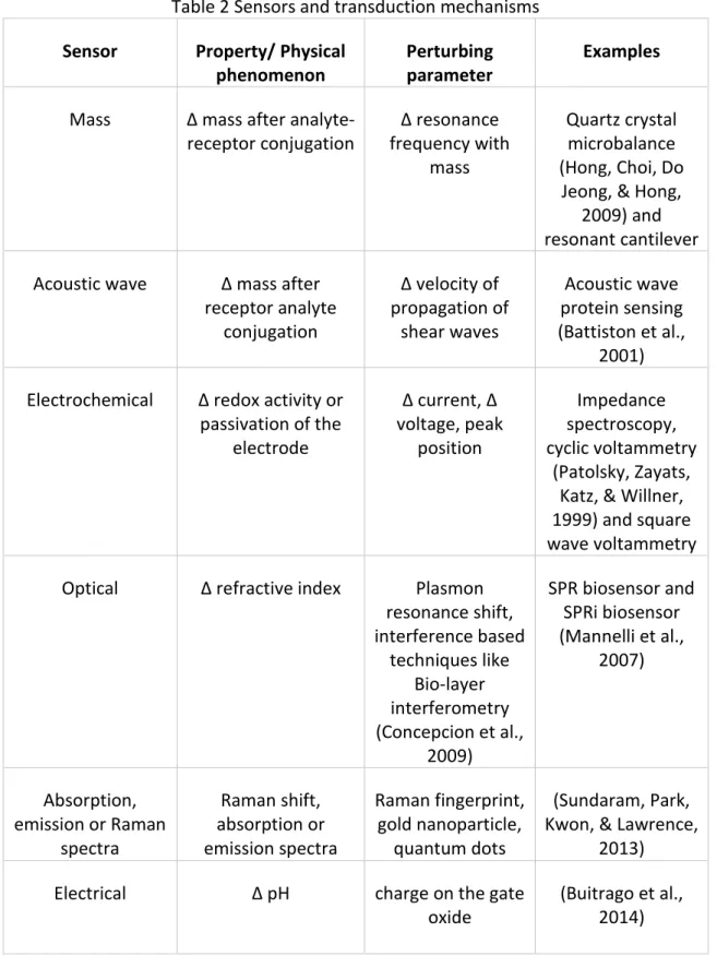
Many of nature’s vast repertoires of physical phenomenon have been used for transduction of sensing events, each of these mechanisms measure specific properties of biomolecules or exploit different physical phenomenon for biosensing. Table 2 shows examples of sensors, the physical property or phenomenon being measured, the transduction mechanism and some examples from literature.
Table 2 Sensors and transduction mechanisms
Sensor Property/ Physical
phenomenon
Perturbing parameter
Examples
Mass ∆ mass after analyte-receptor conjugation ∆ resonance frequency with mass Quartz crystal microbalance (Hong, Choi, Do
Jeong, & Hong, 2009) and resonant cantilever Acoustic wave ∆ mass after
receptor analyte conjugation ∆ velocity of propagation of shear waves Acoustic wave protein sensing (Battiston et al., 2001) Electrochemical ∆ redox activity or
passivation of the electrode ∆ current, ∆ voltage, peak position Impedance spectroscopy, cyclic voltammetry (Patolsky, Zayats, Katz, & Willner, 1999) and square wave voltammetry Optical ∆ refractive index Plasmon
resonance shift, interference based techniques like Bio-layer interferometry (Concepcion et al., 2009) SPR biosensor and SPRi biosensor (Mannelli et al., 2007) Absorption, emission or Raman spectra Raman shift, absorption or emission spectra Raman fingerprint, gold nanoparticle, quantum dots (Sundaram, Park, Kwon, & Lawrence,
2013) Electrical ∆ pH charge on the gate
oxide
(Buitrago et al., 2014)
Surface plasmon resonance (SPR) is a charge-density oscillation that may exist at the interface of two media with dielectric constants of opposite signs, for instance, a metal and a dielectric. The charge density wave is associated with an electromagnetic wave, the field vectors of which reach their maxima at the interface and decay evanescently into both media (Sundaram et al., 2013). This surface plasmon wave (SPW) is a TM-polarized wave. These waves are sensitive to the dielectric environment close to the interface. Detection of Vibrio cholera O1 (Sundaram et al., 2013) was demonstrated with SPR using gold on BK 7 glass plates functionalised with 11-mercaptoundecanoic acid and hexanethiol, activated with NHS/EDC, protein G and Mab against V. cholerae. The detection range was found to be 105/mL to 109/mL.
Impedance spectroscopy is a small-signal measurement of the linear electrical response of a material of interest and the subsequent analysis of the response to yield useful information about the physicochemical properties of the system. Analysis is generally carried out in the frequency domain (Macdonald, 1992). E. coli are bacteria that naturally occur in the intestinal tracts of humans and warm-blooded animal. One pathogenic strain, E. coli O157:H7, produces toxins that damage the lining of the intestine, cause anemia, stomach cramps and bloody diarrhea, and serious complications called hemolytic uremic syndrome (HUS) and thrombotic thrombocytopenic purpura (TTP). Radke et. al. (Radke & Alocilja, 2005) have demonstrated detection of E. coli O157:H7 in culture and inoculated food samples, down to 104 CFU/mL, using
impedance spectroscopy on an inter-digitated electrode array and polyclonal antibody immobilized as the recognition element.
Detection of paramagnetic particles labeled L. monocytogenes has been demonstrated by Grossman et. al. using high-critical temperature superconducting quantum interference device (SQUID), which are extremely sensitive to detect magnetic flux. This was used to measure binding between antibody-linked magnetic particles and bacteria, a pulsed magnetic field is used to align the magnetic dipole moments and use a high-critical temperature SQUID, to measure the magnetic relaxation signal when the field is turned off. Unbound particles randomize direction by Brownian rotation too quickly to be detected. In contrast, particles bound to L. monocytogenes are effectively immobilized and relax in about 1 s by rotation of the internal dipole moment. This relaxation process is detected by the SQUID. The limit of detection of 5.6 ± 1.1 106 mL-1 of
L. monocytogenes has been demonstrated (Grossman et al., 2004).
Raman spectroscopy is based on inelastic scattering of photons following their interactions with the vibrating molecules of the sample. During this interaction, photons transfer (Stokes)/receive (Anti-Stokes) energy from molecules as vibrational energy. Thus the energy change of the scattered photons correspond to the vibrational energy of the sample molecules (Notingher, 2007). Raman scattering can also be enhanced (~1010) using metal nanostructures, this forms the
basis of surface enhanced Raman spectroscopy (SERS). Food safety is dependent upon the ability to detect and differentiate foodborne pathogens that cause severe outbreaks. Major outbreak in food is caused by foodborne pathogenic bacteria such as Salmonella spp., Staphylococcus spp.,
Shigella and Escherichia coli, Bacillus spp. and Clostridium spp. Sundaram et. al. (Sundaram et al.,
pathogen detection and classification. A summary of detection limits and analysis time for
Legionella pneumophila is given in table 3.
Table 3 Detection limits and time for analysis for different methods of detecting Legionella
pneumophila.
Duplan et. al. (Duplan, Frost, & Dubowski, 2011) have demonstrated detection of E. coli bacteria using the effect of bacterial electrostatic interaction with GaAs/AlGaAs NH. The biochips were functionalized with self-assembled monolayers of alkanethiols and polyclonal biotinylated antibodies immobilized with neutravidin. A shift in the position of PL maxima was correlated with different concentrations of E. coli in the investigated aqueous solutions.
Sensor Detection
Limit
Time for
analysis Disadvantages
Fiber based immunosensor (Lin et al.,
2007) 10 CFU/mL 1 – 2 hr
Requires specially polished fiber
Surface acoustic wave (Howe & Harding, 2000)
106
cells/mL 3 hr
Whole cell.
Specially built SAW sensors SPR (Manera et al., 2013) 103 CFU/mL 60 min Bulky equipment
RTPCR (Ballard et al., 2000) 2.5 CFU/mL 90 min Bulky equipment Auto fluorescence of Legionella at 450
nm (Ishii et al., 2013) 106 /mL -
Insufficient detection limit and non-specificity Lateral flow assays (Manera et al.,
2013)
9.2 x 10³
CFU/mL 20 min Large variability Immunofluorescence and solid phase
cytometry (Parthuisot et al., 2011) 0.034 /mL >60 min
Complicated and possibly bulky
Surface enhanced raman spectroscopy (Knauer, Ivleva, Niessner, & Haisch,
2010)
5 x 10³
CFU/mL 1 min
Electrokinetic
concentration required, the SERS reader is bulky Culture (Ditommaso, Giacomuzzi,
Gentile, & Zotti, 2010)
0.08
4 GOALS OF THIS WORK
The preliminary work performed in the QS Group was focused on detecting bacteria using GaAs functionalized with various alkanethiol self-assembled monolayers (SAM) used as an anchor for immobilization of antibodies and passivation of the GaAs surface against corrosion. During the experiments that I had undertaken with Elnaz Nazemi, it became obvious that the stability of GaAs/AlGaAs biochips suffered from the photocorrosion effect. Consequently, the question was asked: could the photocorrosion process be controlled with a precision that would allow observing perturbations induced by electrically charged molecules immobilized at the semiconductor surface or in its proximity? This has led us to the discovery of a digital photocorrosion (DIP) based “Photo-electochemical biosensing method” that is a subject of a recently allowed US patent (Jan J Dubowski, Nazemi, Aithal, & Huang, 2018).
The primary goal of this work was to explore DIP dependent PL of GaAs/AlGaAs heterostructures for monitoring in situ the decomposition process of these materials with an atomic layer resolution. The goal was also to develop a semi-quantitative model of this process. I was targeting the identification of the relationship between the photocorrosion rate, photon flux and type of aqueous environments employed for supporting the photocorrosion process. I have applied the PL effect for room-temperature metrology of GaAs/AlGaAs NH.
Expecting a difference between the surface potential of GaAs and AlGaAs exposed to the same aqueous environment, I carried out open circuit potential (OCP) measurements of GaAs/AlGaAs photocorroding in water and weak solutions of chlorides. This resulted in the demonstration of an excellent correlation between in situ revealed interfaces with PL and those with OCP. The significance of this result is that is suggests the possibility of atomic-level metrology of materials that do not show room-temperature measurable PL.
The final goal of this work was to investigate application of the DIP effect for detection of live
Legionella pneumophila in water and phosphate buffered saline (PBS) solution. Due to the
pathogenic nature of these bacteria, the related experiments were carried out in a dedicated bio-security level 2 laboratory of the Interdisciplinary Institute for Technological Innovation (3IT).
5 EXPERIMENTAL METHODS AND TOOLS
The following sections describe samples investigated in this work, and they provide discussion of the protocols employed for sample preparation and carrying out diagnostics. A brief description of experimental setups is also provided in this chapter.
5.1 Semiconductor samples
Semiconductor wafers were grown either by molecular beam epitaxy (MBE) or metalorganic chemical vapor deposition (MOCVD). MBE allows for atomic layer controlled growth of single crystal semiconductors from vapour phase precursors in ultra-high vacuum. In contrast, MOCVD growth occurs by a chemical reaction of the metal organic precursors under near-atmospheric pressure. The MOCVD growth rates could be four or five times faster than those of MBE, but MBE has better control of background carrier concentration than MOCVD (Sturdivant & Harris, 2015). The investigated GaAs/AlGaAs NH were grown on double side polished semi-insulating GaAs (100) wafers by MBE (Wafers 10-150, v0803 and AXT14-287) and by MOCVD (Wafer 10-413). Each of these wafers have a 200 nm or 500 nm thick epitaxial layer of GaAs, as well as a superlattice with 2.4 nm thick AlAs and 2.4 nm thick GaAs that were grown in each case on GaAs substrates as defect reduction buffer layers (Dawson & Woodbridge, 1984).
Fig. 4 Schematic of the investigated heterostructures used in this work and their corresponding PL emission spectra. Wafer 10-150 (a), v0803 (e), and AXT14-287 (i) have their PL emission maxima at 869 nm. Wafer 10-413 (c) is a QW microstructure that emits at 829 nm (d). Wafer JD2C (g) a QW microstructure with emission at 850 nm (h).
Wafers 10-150, v0803 and AXT14-287, whose structure are given in figure 5 (a), (b) and (g) have room-temperature PL emission maxima at 869 nm and no quantized emission was observed from these wafers at room temperature. Whereas 10-413, figure 5(c), has its PL maximum at 829 nm that originates from 6-nm thick QWs. A weaker PL emission observed at 869 nm, as shown figure 5 (d), originates from a 200-nm thick GaAs layer. The wafers were spin coated with photoresist (S1813, Shipley), mounted on a carrier tape and diced into 2 mm x 2 mm or 4 mm x 4 mm chips. Such samples, before direct measurements, or before surface functionalization, were sonicated in semiconductor grade OptiClear (National Diagnostics), acetone (ACP Chemicals, Canada) and isopropyl alcohol, to remove photoresist used to reduce particle contamination on samples’ surfaces.
5.2 Photoluminescence
5.2.1 Basic principle
Optical excitation of the semiconductors with photons above the bandgap energy (Eg), results in
the generation of electron-hole pairs. In direct bandgap semiconductor, excitation can occur without the interaction of a phonon as shown in figure 5, whereas in indirect bandgap semiconductors, the phonon assisted (hω) excitation is necessary. A well-known example of an indirect bandgap material is Si. All microstructures investigated in this work represent direct bandgap materials.
Fig. 5 Energy (E) – momentum (k) diagram showing absorption of photon in a direct bandgap and indirect bandgap semiconductor (Van De Krol, 2012). In this figure, ω is the frequency of a phonon, k is the momentum and ν the frequency of the photon.
Lifetime of excited minority charge carriers determine the PL emission efficiency in a semiconductor. Carrier generation and recombination processed determine the carrier lifetime in a semiconductor. PL emission increased follows increased carrier lifetime and vice versa. For a semiconductor with two interfaces, for example, GaAs sandwiched between two AlGaAs layers, minority carrier lifetime, τ could be described by the following equation (Ahrenkiel et al., 1989):
1 𝜏
=
1 𝜏𝑅+
1 𝜏𝑛𝑅+
2𝑆 𝑑 Equation 3where τR is the radiative recombination lifetime, τnR the non-radiative recombination lifetime, S
denotes the surface recombination velocity, and d is the depletion width. Except for S and d, the other components in this equation are bulk parameters of the semiconductor. The S represents the non-radiative recombination component due to the break in the translational symmetry of the semiconductor at its surface. Decreased S increases the minority carrier lifetime, and hence the efficiency of PL emission.
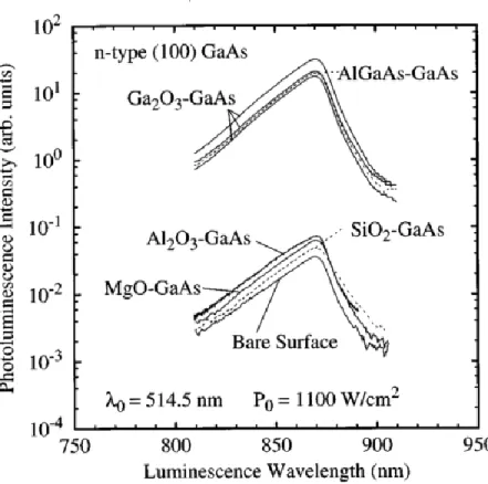
Oxidation at GaAs surface has been shown to result in increased efficiency of PL emission from GaAs. While coating GaAs surfaces with oxides of Al-, Si- and Mg resulted in S comparable to that of bare GaAs. i.e., ≈ 107 cm/s, the Ga
2O3-coated GaAs showed S as low as 4000-5000 cm/s.
The related PL spectra of GaAs are shown in figure 6 (Passlack, Hong, Mannaerts, Kwo, & Tu, 1996).
Fig. 6. PL spectra for GaAs and AlGaAs grown with molecular beam epitaxy, coated with various oxides (Passlack et al., 1996).
It can be seen that PL intensities are similar for uncoated GaAs and GaAs coated with Al2O3, MgO,
SiO2 oxides. However, Ga2O3 coated GaAs and AlGaAs coated GaAs have PL emission about 100
times that of bare GaAs.
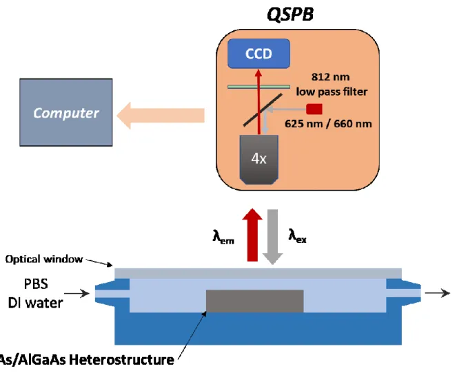
In general, PL provides the information about electronic states of a semiconductor with the intensity and spectral characteristics of the emitted photons depending on the radiative and non-radiative processes in the semiconductor. In this work,PL measurements were performed using either a Hyperspectral Imaging Photoluminescence Mapper (HIPLM) or a custom designed Quantum Semiconductor Photonic Biosensor (QSPB) Reader described in (Kim et al., 2009) and (Aziziyan et al., 2016; Nazemi et al., 2015), respectively.
5.2.2 Photocorrosion setup
The experimental setup designed for photocorrosion of samples and simultaneous collection of PL data consists of:
a) A reservoir with investigated fluids (DI H2O, NH4OH, PBS and biological targets)
b) A flow cell module for mounting investigated GaAs/AlGaAs microstructures (chips) c) An optical setup designed to irradiate samples and collect PL signal emitted by the samples d) A peristaltic pump for injecting fluids to the flow cell
A fluidic flow cell, custom machined from a solid PEEK (Polyetheretherkeone), was designed to hold samples of dimensions up to 4 mm x 4 mm. The flow cell was connected with the reservoir and the peristaltic pump (Masterflex L/S) using Viton tubing, the system block diagram is illustrated in figure 7. The pump allowed for precise flow rate control. Typical flow rates used in these experiments were at 0.1 mL/min.
In the HI-PLM measurement setup, the sample is excited with a continuous wave diode pumped Nd:YAG laser emitting at 532 nm wavelength. Two volume Bragg gratings allow measurement of spatio-spectral emission characteristics of samples. Spectral resolution of 2 nm and spatial resolution under 2 μm can be achieved. The typical excitation power at the sample was 25 mWcm- 2, temporal variation in laser power is monitored using a photodiode. The samples
were excited with intermittent pulses using a shutter. This intermittency was defined by a “duty cycle” (DC) parameter: TON / (TON + TOFF).
The excitation in QSPB was provided either by a LED source (625 nm / 660 nm) or by a halogen lamp. An 812-nm cut-off long pass filter (Thorlabs FELH800) was applied in the QSPB Reader to prevent the excitation photons from reaching the CMOS detector employed for detecting PL emission. A schematic of QSPB and flow cell setup for PL measurements is illustrated in figure 8. A dedicated glass window facilitates excitation of samples and collection of PL data. The excitation power density measured at the sample surface in the QSPB systems ranged between 20 - 150 mW/cm2.
Fig. 7. Fluidic system block diagram
Reservoir
Peristaltic
Flow Cell
Fig. 8 A schematic view of the QSPB and flow cell setup.
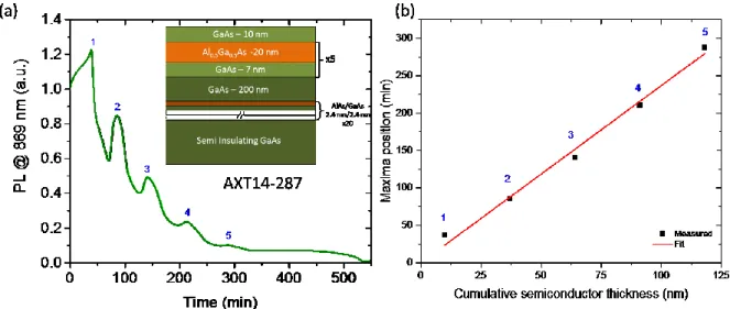
Example of a temporal PL plot collected from a 2 mm x 2 mm chip of the AXT14-287 wafer exposed to an ammonia environment and irradiated with 25 mW/cm2 at 660 nm for 1 s in each 10 s period
(duty cycle 1 s/10 s) is shown in Fig. 8. The chip was cleaned as described in the previous section and placed inside a flow cell with 28% NH4OH solution. The temporal PL plot of this microstructure
reveals 5 maxima clearly observed in figure 9(a) and the PL maxima vs cumulative thickness of the NH is shown in figure 9(b).
Fig. 9 Time dependent PL emission (at 869 nm) of a GaAs/AlGaAs NH (sample AXT14-287) immersed in NH4OH and irradiated in QSPB with a 660 nm LED at DC = 1 s/100 s (a), and a plot
of the position of PL maxima vs. cumulative thickness of the NH (b).
The maxima positions are linearly correlated with the microstructure thickness up to ~ 120 nm (known from the epitaxial growth parameters). The average etch rate of this chips is estimated at 0.4 nm/min or 0.66 nm per 1 cycle of photo excitation, which corresponds approximately to 2.3 monolayer of the microstructure removed each cycle. Details of this process and interpretation of the observed PL maxima are provided in Chapter 6.
5.2.3 Detection of electrically charged molecules using DIP
The DIP process is driven by the surface concentration of hole (h+) as discussed in section 2.2.2.
The near electric field in the depletion layer of the semiconductor modulates the rate of hole (h+)
transport to the semiconductor surface during DIP (Mannheim, Alkire, & Sani, 1994) (Miller & Richmond, 1997) . Thus, the presence of electrically charged molecules immobilized in the proximity of the semiconductor surface is expected to influence the rate of photocorrosion. A vast majority of bacteria are negatively charged in aqueous environment (A. T. Poortinga et al., 2002) and DIP could be used as a transduction mechanism for detection of this charge. Nazemi et. al. have demonstrated detection at 103 CFU/mL of E. coli K12 in PBS (Nazemi et al., 2015). The
GaAs/AlGaAs samples were coated with E. coli antibody using alkanethiols. Such samples were exposed to varying solution concentrations of E. coli K12. Fig. 10 illustrates the PL peak position for solutions with different concentrations of E. coli K12. A logarithmic response is demonstrated between 103 and 105 CFU/mL of E. coli K12. Additionally, a negative control with Bacillus subtilis
at 105 CFU/mL is also shown. In the current work, this approach is extended to Legionella
Fig. 10 PL peak position vs. different concentrations of E. coli K 12 bacteria (Nazemi et al., 2015).
5.3 Biofunctionalization
5.3.1 Sample surface preparation
The GaAs functionalization procedure is based on previously published work by Duplan et. al. (Duplan et al., 2011) and Nazemi et al. (Nazemi et al., 2015) . 2 mm x 2 mm diced samples of the nano-heterostructure are sonicated sequentially in Opticlear, acetone and isopropyl alcohol (IPA), for two minutes each. Subsequently, the native oxide of GaAs is etched with 28% ammonium hydroxide solution for two minutes, transferred to degassed ethanol containing the thiol mixture and incubated overnight in darkness. Preparation of thiol in degassed ethanol is necessary to avoid oxidation of GaAs. The thiolated samples are rinsed with ethanol.
5.3.2 SAMs formation on GaAs
Biorecognition layer is a critical element of a biosensor. In the case of antibody based sensors, one of the most controllable methods of formation of this layer is based on using self-assembled monolayers (SAM) of alkanethiols. Self-assembly of alkanethiols (R-SH) on gold and semiconductors such as GaAs leads to formation of an ordered, compact monolayer on the underlying substrate. This process has been studied for decades (Ding, Moumanis, Dubowski, Tay, & Rowell, 2006; J. J. Dubowski, Voznyy, & Marshall, 2010), and has been applied for biosensing (Wink, J. van Zuilen, Bult, & P. van Bennekom, 1997), photolithography (Tiberio et al., 1993) and
passivation of GaAs (Cuypers et al., 2016). The theoretical maximum surface coverage with alkanethiol SAM on GaAs (100), estimated by density function theory (DFT) calculation was found to be 50 % (Voznyy & Dubowski, 2008). This has an implication for the ability to protect the GaAs surface against corrosion or photocorrosion.
Typically, Al0.35Ga0.65As/GaAs QSPB biochips are functionalized with a mixed SAM architecture
that consists of a short chain hexadecanethiol (HDT, 15 CH2 backbone with a terminal CH3
(methyl)) mixed with a biotinylated polyethylene glycol thiol (PEG-b, 11 CH2 backbone with 3
ethylene glycol groups and, biotin or Sulphur at each extremities) at 1:14 (v/v). The short chain HDT acts as a spacer to reduce the steric hindrance of the formed self-assembled monolayer. A schematic view of a HDT/PEG-b- architecture employed for attaching neutravidin and biotinylated antibodies is shown in figure 11.
5.3.3 Antibody conjugation
The samples coated with HDT/PEG-b- architectures were rinsed with 1xPBS to remove any residual ethanol and exposed to 0.2 mg/mL of neutravidin for two hours in an environment without light. Next, they were rinsed with 1xPBS, exposed to a 0.1 mg/mL solution of Biotinylated antibody for one hour and, finally, exposed to a PBS solution containing the bacteria. Figure 11 shows a schematic of the architecture after bacterial binding.
5.4 X-ray photoelectron spectroscopy
X-ray photoelectron spectroscopy (XPS) is a surface analysis technique for determination of composition as well as the chemical states of surface constituents (Turner & Schreifels, 2000). Figure 12 (a) shows a schematic of the method. Monoenergetic soft x-ray photons are absorbed
by core electrons and are ejected from the atoms constituting the sample surface. The x-ray photons have an absorption depth of 1-10 µm and electrons are excited within this range (Moulder, Stickle, Sobol, & Bomben, 2002). A vast majority of these electrons do not leave the material and only the kinetic energy of the electrons emitted from the surface atoms, typically within about 8-10 nm from the surface are measured. The energetics of the emitted electrons are illustrated on figure 12 (b) and relation between energies given by the following equation:
KE stands for kinetic energy of the emitted electron,
ℎ𝜈
the energy of the x-ray photoelectron, BE the binding energy,ℎ
Plank constant andф
𝑠the spectrometer work function. These measurements are performed under vacuum, usually a low-resolution “survey scan” in performed for the presence of constituent elements, and afterwards a high-resolution scan is performed along the peaks of interest. In semiconductors, XPS is routinely used to measure the constituent elements, contaminations, oxidation states (Liu, Huang, & Dubowski, 2014), thickness of nanometer layers (Huang & Dubowski, 2014) and location of band edges (Nesher et al., 2006). Grazing angle incidence is a technique used to increase depth resolution of XPS (Chester & Jach, 1993). XPS measurements in this work used grazing angle incidence, 60o from the normal, whichallowed to increase depth resolution to under 1 nm (Kerr et al., 2014).
𝐾𝐸 = ℎ𝜈 − 𝐵𝐸 − ф
𝑠 (4)Fig. 12 Schematic of XPS measurement setup (a) and energetics of the XPS process (b).
X-ray Source
hν
Detector
e-e-
e-1-10nm(a)
(b)
Valence Band hν Ef Ev Photoelectron Core hole Core levels Kinetic Energy (KE) Binding Energy (BE)5.5 Fourier transform infrared spectroscopy
Fourier transform infrared spectroscopy (FTIR) is a popular technique for chemical analysis of thin films and studying chemical composition of the surface coating chemical compounds. Infrared (IR) absorption spectra correspond to the vibrational energy of the molecule and the number of absorption peaks correspond to the degrees of freedom of the molecule. IR radiation excite molecules to a higher energy state. The excited states result in the vibrations of molecular bonds occurring at varying wavenumbers in the IR region of the light spectrum. The wavenumber of each IR absorbance peak is determined by the intrinsic physicochemical properties of the corresponding molecule, and is thus diagnostic, like a fingerprint of that particular functional group (Chen et al., 2015). IR spectroscopy has routinely been used to probe the structure of SAMs formed on noble metals and semiconductors (Hostetler, Stokes, & Murray, 1996). The FTIR measurement setup consists of an IR source, beam splitter, stationary and moving mirrors as shown in figure 13. The beam from the interferometer interacts with the sample and is measured by the detector. This signal is processed to obtain the IR absorption spectra.
The fundamental modes of operation are reflectance, transmission and attenuated total reflection (ATR). Reflectance mode of operation is suitable if the sample has a measurable reflection in the IR range of the spectrum (works well for metals), transmission mode could be used if the sample is mostly transparent in the IR and finally ATR is a special mode used to probe surface properties of material. In the ATR mode, the IR radiation undergoes total internal reflection in a crystal that remains in contact with the sample, which allows to probe a sample with an IR evanescent wave that interacts with the sample. In this work, a Bruker Hyperion 2000 FTIR-microscope system has been used in a transmission mode. This system consists of a Bruker RockSolid interferometer, a Globar mid-infrared source with emission between 6000 to 10 cm- 1,
liquid nitrogen cooled mercury, cadmium, and telluride detector, and a motorized x-y stage. A Fig. 13 FTIR setup in the transmission mode.
IR Source Detector Stationary Mirror Moving Mirror Beam splitter Sample
15x objective was used to interrogate a 0.5 mm diameter area of the 2 mm x 2 mm sample, each measurement was performed with 4 cm-1 resolution and averaged over 256 scans.
The stability of SAMs on a photocorroding surface was studies using FTIR. The thiol SAMs were prepared with mercapto hexadecanoic acid thiols (MHDA), as a model thiol. 2 mm x 2 mm samples of the 10-413 wafer were cleaned with Opticlear, acetone and isopropanol. These samples were dried with nitrogen and etched with ammonium hydroxide for two minutes. After rinsing with degassed ethanol, samples were incubated in 2 mM MHDA overnight and rinsed with degassed ethanol. Photocorrosion was performed on such samples in DI water under QSPB2 with 20 mW/cm2 excitation intensities and 3 s /25 s DC and photooxides were removed
by incubating with NH4OH for 10 min. IR absorption spectra were measured as described earlier.
An example of FTIR study of the SAM layer of 16-mercaptohexadecanethiol on GaAs, is shown in figure 14 (Huang et al., 2013). This work by Huang et. al. investigated the effect of mixture of solvents on formation of SAM. The high resolution FTIR spectra corresponds to the asymmetric (~2918 cm-1) and symmetric (~2850 cm-1) vibration of CH
2 group for varying mixtures of
ethanol/water. Comparison of peak position and absorbance corresponding to CH2 asymmetric
vibrations, provides evidence of increased quality of SAM with addition of water to an ethanol solution.
Fig. 14 FTIR spectra of SAM on GaAs corresponding to symmetric and asymmetric vibrations of CH2 (Huang, Liu, Moumanis, & Dubowski, 2013).
6 RESULTS AND DISCUSSION
In the following section, we describe the results and discussions pertaining to photocorrosion metrology, application of the open circuit potential for monitoring of the digital photocorrosion process and the use of digital photocorrosion for detecting bacteria.
6.1 Foreword: Article 1, Photocorrosion metrology of
photoluminescence emitting GaAs/AlGaAs heterostructures
The paper published in Journal of Physics: Applied Physics D demonstrates for the first time, the digital photocorrosion (DIP) dependent photoluminescence (PL) of GaAs/AlGaAs heterostructures for monitoring in situ the decomposition process of these materials with an atomic layer resolution. This paper established the relationship between the photocorrosion rate, photon flux and type of aqueous environments employed for supporting the photocorrosion process. Application of DIP for metrology of nanoheterostructures (NHs) has been demonstrated and provides insights into the processes that are applied for detection of bacteria.
Authors:
Srivatsa Aithal: PhD candidate Neng Liu: PhD candidate Jan J. Dubowski: Professor
Affiliation:
Laboratory for Quantum Semiconductors and Photon-based BioNanotechnology, Interdisciplinary Institute for Technological Innovation (3IT), Department of Electrical and Computer Engineering, Université de Sherbrooke
Date of publishing: 19 December 2016
Reference:
Aithal, S., Liu, N., Dubowski, J.J., “Photocorrosion metrology of photoluminescence emitting GaAs/AlGaAs heterostructures”, J. Phys. D: Appl. Phys. 50 (2017) 035106 (9pp)
Titre: Métrologie de photocorrosion de photoluminescence des hétérostructures GaAs/AlGaAs Résumé: La sensibilité élevée de l'effet de photoluminescence (PL) aux états de surface et aux
réactions chimiques sur les surfaces de semi-conducteurs émetteurs de PL s'est révélée intéressante pour le monitoring de la micro-structuration photo-induite de tels matériaux. Pour résoudre les problèmes de gravure à des taux d’enlèvement à l’échelle nanométrique, nous avons