HAL Id: hal-01240244
https://hal.archives-ouvertes.fr/hal-01240244
Submitted on 8 Dec 2015
HAL is a multi-disciplinary open access
archive for the deposit and dissemination of
sci-entific research documents, whether they are
pub-lished or not. The documents may come from
teaching and research institutions in France or
abroad, or from public or private research centers.
L’archive ouverte pluridisciplinaire HAL, est
destinée au dépôt et à la diffusion de documents
scientifiques de niveau recherche, publiés ou non,
émanant des établissements d’enseignement et de
recherche français ou étrangers, des laboratoires
publics ou privés.
Private Circuits II versus Fault Injection Attacks
Henitsoa Rakotomalala, Xuan Thuy Ngo, Zakaria Najm, Jean-Luc Danger,
Sylvain Guilley
To cite this version:
Henitsoa Rakotomalala, Xuan Thuy Ngo, Zakaria Najm, Jean-Luc Danger, Sylvain Guilley. Private
Circuits II versus Fault Injection Attacks. Reconfig 2015, Dec 2015, Mayan Riviera, Mexico.
�hal-01240244�
Private Circuits II versus Fault Injection Attacks
Henitsoa Rakotomalala
∗, Xuan Thuy Ngo
∗, Zakaria Najm
∗, Jean-Luc Danger
∗†, Sylvain Guilley
∗†,
∗ Institut MINES-TELECOM, TELECOM ParisTech, CNRS LTCI (UMR 5141).
† Secure-IC S.A.S., 15 Rue Claude Chappe, Bˆat. B, ZAC des Champs Blancs, 35 510 Cesson-S´evign´e, FRANCE.
Abstract—Cryptographic implementations are subject to phys-ical attacks. Private circuits II is a proven protection against a strong attacker, able to read and write on a finite number of chosen internal nodes. In practice, side-channel analyses and fault injections are less accurate: typically, classical injection techniques (clock and power glitches, electromagnetic pulses, etc.) can be reproducible, but they do not allow to choose the targeted nodes (the situation is different for software dual-rail with precharge logic, such as [1], [2], where (0, 1) ↔ (1, 0) bitflips are easier to achieve, since the computation is fully sequentialized [3]). So, a priori, private circuits II should be a secure protection against such classical fault injection attacks. In this paper, we provide the first implementation of private circuits II in FPGA, secure against read and/or reset of one internal wire chosen by the attacker. Our implementation is a manually coded netlist which instantiates LUT6 2 (with dual outputs, as required for private circuits II). Our design is a SIMON block cipher programmed in a Spartan 6 Xilinx FPGA. It features a throughput of 142 Mbit/s. We perform a security analysis, and notice that some exploitable ciphertexts can be outputted despite the countermeasure. Our analysis reveals that correlated faults exist because LUT6 2 outputs are produced almost simultaneously. In particular, the critical path actually consists in a dual-rail pair, which is consistently faulted together. If this pair is late with respect to the clock rising edge, then the previous value can be latched instead of the new one. Such fault behaves like a toggle ((01)2 becomes(10)2 or vice-versa) of licit
values. They propagate to the ciphertext which becomes by the same token susceptible to a differential fault attack. Nonetheless, we emphasize that such faults require a steady fault injection setup: otherwise, multiple critical paths are violated, resulting in non-exploitable (fully zeroized) ciphertexts.
Index Terms—Private circuits II; Fault injection attack; Cor-related faults on dual LUT6 2 outputs; Fault effect analysis with ChipScope.
I. INTRODUCTION
Cryptographic keys are safeguarded in secure hardware de-vices. Now, implementation-level attacks threaten the security of such sensitive devices. Those attacks can be classified in two categories: passive and active. Passive attacks are also known as side-channel attacks, and consist in collecting physical measurements leaked through the boundary of a device. Such leakage contains information about the internal variables handled by the device, which can be sufficient to extract secret keys. Active attacks rely on perturbations to force the device malfunction. Depending on the way the errors propagate within the device, the faulted output might reveal information about the keys.
Henitsoa Rakotomalala is the corresponding author. This project has been funded by Google compagny
Obviously, it is important to protect devices against such attacks. It is admittedly hard to completely prevent them, let alone because of the overhead incurred by countermeasures. Thus tradeoffs between security and cost must be devised. The ideal situation is when a security parameter allows to quantify the achieved security level.
Private circuits is the most acknowledged way to provably instantiate a countermeasure with clear and meaningful se-curity parameter(s). Actually, private circuits appeared in the literature in two steps, namely private circuits I (PC-I, [4]) and private circuits II (PC-II, [5]). The aim of PC-I is to protect only against passive attacks. The attacker is assumed to be able to read k wires within a digital circuit, thereby collecting k bits of information per clock cycle. PC-I is a constructive method which shows how to design a circuit which resists the eavesdropping by such attacker. The rationale is to entangle random bits with the design so as to have any tuple of k wires be independent from the (unmasked) sensitive values. Now, attackers can also be active, and attempt to modify wires in the circuits. This is the motivation for PC-II: this time, a design method to resist against an attacker who is able to read k chosen wires and overwrite t chosen wires is proposed. The write operation might be of two types: only reset, or set
to an arbitrary chosen value. The pair (k, t) is the security
parameter of PC-II; whatever this pair, PC-II is able to generate an implementation which is provably secure. The PC-II style adds redundancy to the netlist in such a way that any change to 1, . . . , t wires will cause an erasure of data after passing
through a logic gate. For instance, when t= 1, the redundancy
is the same as dual-rail with precharge logics [6, Chap. 7], where bit0 (resp. 1) is encoded as (01)2 (resp.(10)2), whilst
(00)2 and (11)2 are illicit values used by PC-II as possible
erased values.
Today, circuits are difficult to probe due to several reasons: first of all, the number of metal layers is huge (> 10) for the latest CMOS technologies. Accordingly, chip designers take proactive protection of sensitive signals by burying them, which makes them less accessible by a probing station. Be-sides, backside probing is also chancy because it is hard to know (at a resolution of a few tens of nanometers) what can be probed blindly through the silicon wafer. Additionally, backside probing requires costly equipments (called Focused Ion Beam stations), which are expensive and feature a non-negligible risk of permanently damaging the circuit [7]. Sec-ond, some technological protections (sensors of circuit lid opening, shields, etc.) attempt to detect probing attacks.
side-channel and perturbation attacks. Typically, state-of-the-art lab equipments allow to collect side-channel information without contacting the device. Power analyses only need an external monitoring of the amount of current flowing through the cir-cuit, while electromagnetic analyses can be conducted even far away from the circuit. Fault injection attacks like overclocking or underfeeding do not allow to predict exactly their effect: the faults can be injected at multiple unpredictable locations inside the chip. Although slightly more local, electromagnetic pulse injection has also a coarse area of influence.
In this context, it is interesting to evaluate the suitability of PC-I and PC-II countermeasures against such macroscopic (by opposition to the microscopic scale of probing attacks) attacks. In theory, protecting against an attacker who can probe one wire is sufficient to protect against a first-order attacker, who exploits only the aggregated and noisy leakage from parts or totality of the chip. The same argument applies to active attacks: a protection which resists arbitrary access to carefully
selected (6 t) wires can, all the more, protect against an
attacker who is less accurate in the injected faults of same multiplicity (6 t).
But the study is still worthwhile. For instance, due to im-plementation constraints, some requirements of private circuits design style are hard to meet. This has already been demon-strated on PC-I implementations, where gates are assumed to evaluate in a precise order. However, it is known that unless every gate is made synchronous, glitches can occur which break the correct evaluation order requirement [8].
Contributions: In this paper, we specifically focus on the practical evaluation of PC-II. Our contributions are three-fold. First of all, we implement for the first time a block
cipher using PC-II, using security parameters k= t = 1. This
choice for the security parameters implies the use of random
bits in each gate (since k > 0 for PC-I), and an encoding
of each bit of the PC-I netlist as a dual-rail (since t = 1,
value 0 / 1 in PC-I becomes (01)2 /(10)2 in PC-II). Second,
we identify a weakness in our security assumption, which creates an exploitable vulnerability. Shortly, as PC-II is built on top of PC-I, PC-II inherits implementation constraints from PC-I; in particular, to avoid glitches, PC-II must be mapped such that dual-rail signals are balanced. We leverage on the dual outputs of LUT6 2 in FPGA to meet this constraint. However, such implementation opens the door to correlated faults, whereby both outputs of a LUT6 2 are faulted together.
This negates the attacker model (t= 1 < 2). However, our a
priori security analysis convinced us that it was apparently difficult to obtain correlated faults of multiplicity two in the practical setting of overclocking, underfeeding, or strong electromagnetic (EM) fields injection. Third, we demonstrate an analysis and an attack platform where we can assess experimentally the likelihood of correlated faults to happen and to propagate successfully to the output of the cipher, using overclocking, underfeeding, and EM injection, and with the assistance of an internal FPGA debugger (ChipScope Pro
feature of Xilinx). In practice, for 50% of the plaintexts,
we manage to generate an exploitable faulted ciphertext with
carefully tuned fault injection parameters.
Outline of the paper: The rest of the paper is structured as follows. Section II tackles the private circuits II principle and implementation results in FPGA. Security analysis of PC-II is conducted in Sec. III. Fault injection results are given
and discussed in SectionIV. Finally, SectionVconcludes the
paper and opens some perspectives.
II. PRIVATECIRCUITSI & IIINFPGA
A. PC-I in FPGA, fork= 1
A private circuit I with security parameter k guarantees that any tuple of k wires does not convey any information about a sensitive value. There are several possible protections in the literature, for instance private circuits [4] or stateful private circuits [9]. In the sequel, we focus on the later. Private circuit I implements a notion of Boolean sharing: every bit is represented as a tuple of(2k + 1) wires, such that the bit
value can be recovered by XORing together the(2k +1) wires
values. In the seminal paper [4], a proof of concept is shown based on a netlist which instantiates only few primitives:
• memory elements (typically a DFF), and combinational
functions, namely:
• an “inverter” (INV) gate,
• an “exclusive-or” (XOR) gate and
• an “and” (AND) gate.
The protection consists in replacing those instances by masked gates. Therefore, PC-I can be seen as a transformation from netlist to netlist. The mapping between the unprotected gates
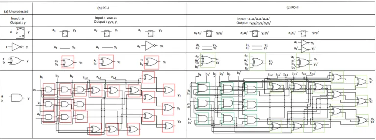
(DFF, INV, XOR and AND) and the PC-I version for k= 1 is
given in Fig.1(a) and (b). Every bit a is thus transformed into a triple(a1, a2, a3), and we notice that the secure evaluation
of the PC-I AND gate requires 3 random bits, denoted as
z1,2, z1,3and z2,3. The netlist transformation is straightforward
because the PC-I transformation is compositional.
It can be seen in Fig.1 (b) that we devote one full LUT6
(represented asred box – see Fig.2(a)) to each gate, despite they have only one or two inputs. The reason is that we want to avoid synthesis optimizations which would (statically) reorder the gates. Obviously, this method is costly in terms of area, but it is guaranteed to be secure. Moreover, this netlist allows us to
quickly implement PC-II (as discussed in next section II-B).
The configuration of the LUT6 for XOR and AND can be found in Tab.I.
We notice that optimization of PC-I (which is out of the scope of our work) has been carried out in the literature in two directions. First of all, Park and Tyagi have improved the mapping of PC-I in FPGA by a better clusterization, without compromising the security [10], [11]. Glitch-free im-plementations have also been demonstrated recently [12], [8]. A convergence between PC-I and threshold implementation (a glitch-tolerant netlist style [13]) has been noticed recently [14].
Second, Rivain and Prouff [15] have adapted PC-I from the
hardware case, which involves Boolean gates (they call PC-I the “PC-ISW” scheme), to the software case, which involves machine words (like bytes). Their work has given rise to
Figure 1. Gates protection in PC-I (with security parameter k= 1) and PC-II (with security parameters k = t = 1) a b y I0 I1 I2 I3 I4 I5 a y b b’ a’ 1 0 O6 O5 y’ LUT6_2 I0 I1 I2 I3 I4 I6 a b LUT6 O y a’ b a’ b a b’ y a b’ y y’ y’ a b y
(a): Mapping in PC−I (b): Mapping in PC−II
Figure 2. Mapping of Boolean functions, (a) in LUT6 as for PC-I, and (b) in LUT6 2 as for PC-II
Table I
CONFIGURATION FORPC-IANDPC-II XORANDANDGATES
Schematic INIT value
PC-I XOR a b y INIT =(6)16 AND INIT =(8)16 PC-II XOR INIT =(24000000420)16 AND INIT =(40000000260)16
many applications, such as masked evaluation of substitution boxes [15], [16], and conversion algorithms between Boolean and arithmetic masking [17].
B. PC-II in FPGA, for k= t = 1
As already mentioned in the introduction, PC-II is a further refinement which enhances PC-I with fault resistance capabil-ity. The constructive method presented in the original paper [5]
assumes several fault models: a predetermined number t of wires can be selected and either reset or set to chosen value, and so at each clock period.
We restrict to the case where the attacker is able to change
the value of t = 1 wire. In this case, the PC-II protection
consists in turning the PC-I circuit into a dual-rail equivalent. This means that:
• each wire x becomes a pair (x, x0), where x0 is the
opposite of x (that is, x0 = ¬x), and that
• each gate is turned into a dual-rail instance (called a
gadget in [5]), as illustrated in Fig. 1(c), where green
boxes are LUT6 2 (cf. Fig.2(b)).
The resistance against one fault arises from this argument: if one bit of a value (x, x0) is corrupted, then the new pair
becomes either (0, 0) or (1, 1). Now, in both cases, the final
faulted value can be obtained irrespective x is equal to0 or 1. The PC-II gates are designed to be infective: should one input be invalid (that is, either (0, 0) or (1, 1)), the gates propagate an invalid(0, 0) value. This behavior of PC-II gates ensures an avalanche of zeroization, thereby preventing the attacker from collecting relevant faulted values at the end of the computation1
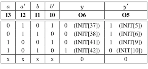
In Xilinx terminology, a LUT6 2 computes simultaneously two outputs named O6 and O5. The configuration of the
LUT6 2 is encoded as a 64-bit integer called INIT [19].
Outputs O6 (resp. O5) execute the function whose truth table
is given by the 32 upper (resp. lower) bits of INIT. We
assign O6 to the true bit x of the dual-rail pair(x, x0) while
O5 is its complementary x0. Despite LUT6 2 has 6 inputs,
four are needed for the PC-II gates. Specifically, the inputs are I0, I1, I2 and I3, whereas inputs I4 and I5 are fixed
1In the original paper on PC-II [5], authors describe in Tab. 2 a cascade
gadgetthat artificially spreads the(0, 0) value over the whole datapath. For the purpose of fault resistance, this is useless, as(0, 0) propagate naturally through computing gates. But in order to have a very datapath-wide check, a simple computation of Hamming weight would be enough [18], [3,§3.1].
Table II
EXAMPLE OF DERIVATION OF THEINITVALUE FOR THEPC-II AND
GATE PROGRAMMED IN ALUT6 2
a a0 b b0 y y0 I3 I2 I1 I0 O6 O5 0 1 0 1 0 (INIT[37]) 1 (INIT[5]) 0 1 1 0 0 (INIT[38]) 1 (INIT[6]) 1 0 0 1 0 (INIT[41]) 1 (INIT[9]) 1 0 1 0 1 (INIT[42]) 0 (INIT[10]) x x x x 0 0 Table III
SYNTHESIS RESULTS FORSIMON 96/96
Unprotected PC-I PC-II
Max. frequency (MHz) 141 77 77 overhead: ./. −45% −45% Registers 96 (<1%) 288 (<1%) 576 (<1%) overhead: ./. +200% +500% LUTs 1063 (1%) 3786 (4%) 5227 (5%) overhead: ./. +256% +392% (LUT6, LUT6 2) (391, 0) (2690, 0) (98, 2592)
to 0 and 1. The exact configuration of PC-II gates is given
in Tab. I. Their construction is detailed in Tab. II for
PC-II AND gate. Apart from licit values, which correspond to (a, a0) ∈ {(0, 1), (1, 0)} and (b, b0) ∈ {(0, 1), (1, 0)}, other
values are mapped to(y, y0) = (0, 0). Such mapping is similar
to that of WDDL noEE [20].
Remarkably, our implementation of PC-I and PC-II consist in the same netlists, let apart the configuration of the LUT masks (INIT values reported in Tab.I).
C. SIMON 96/96 in Private Circuits II
Private circuits are many times larger than their unprotected equivalent. Thus, we considered a lightweight block cipher,
namely SIMON [21]. Interestingly, few studies concern secure
implementation of SIMON (we found only a regular masking
in [22]). We initially intended to implement SIMON [21] in
its 128-bit version. But the overhead of private circuit is huge Thus a version of size of 96-bit for both plaintext and key was implemented on Xilinx Spartan 6 on the SASEBO-W board for the experiment. We notice that SIMON is particularly appropriate for an implementation in private circuits, because it is made only of XOR and AND.
D. Synthesis results for PC-I and PC-II in Xilinx Spartan 6 The synthesis targets a Xilinx Spartan 6 LX150 FPGA constrained to run at clock frequency of 24 MHz (very conservative value). The synthesis results are given in Tab.III. In this table, the red numbers represent the occupied ratio on the FPGA. It clearly appears that the required resources increase when the circuit is implemented in PC-I, and further increase when upgraded to PC-II. Actually, the core resources to implement SIMON are the same for PC-I and PC-II.
Nonetheless, extra logic is required for the interface of PC-I and PC-II to the environment. Now, PC-I requires a wrapper to turn every variable a into a triple (a1, a2, a3). On top
of this wrapper, PC-II needs a conversion between single to dual-rail. So, every bit a is now encoded as a tuple of 6 elements ((a1, a01), (a2, a02), (a3, a03)). The values of the
mask are generated thanks to a linear feedback shift register (LFSR) which yields a vector of size sufficient to feed the necessarily random bits. The LFSR is chosen for a quick implementation and evaluation but we are aware that a good PRNG/TRNG must be used for a real application. These numbers are computed thanks to a polynomial defined by a parameter according to the version of the SIMON. The
throughput of SIMON in PC-{I,II} is96 bit/52 clk ×77 · 106
clk/s ≈142 Mbit/s.
III. SECURITY ANALYSIS OFPC-IIWITHk= t = 1
Obviously, our implementation is secure within the PC-II
model with security parameters k= t = 1, i.e.:
• probing any wire does not disclose any information, and
• modifying any wire can neither be exploited.
Now, we aim to evaluate the resistance of PC-II against fault injection attacks.
A. Setup time violations
Any synchronous circuit must meet timing constraints: the
combinational gatesmust have finished their evaluation before
sequential gates can sample the result they computed. One
can thus define a maximal operating speed for synchronous circuits. Of course, their operation is nominal only within certain environmental conditions, typically in terms of voltage and temperature.
Fault injection attacks consist in displacing the environmen-tal conditions outside of the comfort zone for the circuit. This can be done permanently or transiently. For instance, a strong EM field varying quickly in the vicinity of the FPGA under test can locally create a voltage drop, thereby slowing down combinational gates. As the clock frequency is fixed, the setup time of combinational gates is violated. Symmetrically, the attacker can tamper with the clock, so as to accelerate it. The effect is similar: incomplete computations are sampled in the sequential gates (the DFFs).
If the field of the EM pulse is decreased, then the delays in the combinational paths are reduced. The borderline case is when only one bit in the datapath is faulted. Such situation can be modeled as a single bit-flip error.
B. Timing faults on PC-II witht= 1
In PC-II circuits, a single bit-flip is harmless: indeed, PC-II resists against t= 1 fault.
Now, we argued that EM injection or
overclock-ing/underfeeding are inaccurate faulting methods. Thus, it can be expected that if the stress is slightly increased, the second fault (e.g., bit-flip) will occur on a wire unrelated to the critical path. Hopefully, PC-II is able to withstand such double independent attacks: indeed, two unrelated LUT6 2
gates will output(0, 0) (recall Tab.II), thus zeroizing the rest of the computation (cryptographic computations have a fast diffusion).
Now, in practice, we notice that in dual-rail circuits, the second critical path is actual (very often) the very matching pair of the critical path. Indeed, in a pair(x, x0) of PC-II wires,
the timings are almost balanced.
As argued in Sec. II, the two nets from a same pair pass
through the same LUT6 2, hence have (approximate) balanced timing. More precisely, it is known that balanced routing is hard to achieve in FPGA, because lack of control over the tools and lack of information about the internal structure and delays.
A previous work showed that having the pair of wires pass through the same LUT (by exploiting their dual outputs) can
significantly reduce the unbalance [23]. Indeed, the “graph”
for both wires is the same. Now, unbalances remain as the intra-LUT and LUT-to-LUT delays can vary. Accurate balancing can be achieved with third party tools, such as RapidSmith [24].
Still, for our argumentation, it is sufficient to know that dual-rail pairs have similar delays. Hence they are very likely to be faulted simultaneously upon setup time violations.
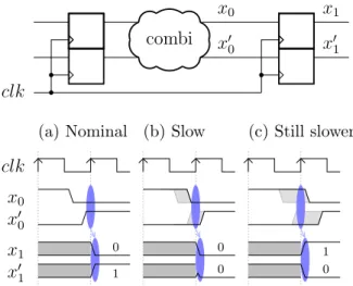
Such intrinsic problem of dual-rail circuits is illustrated
in Fig. 3. It shows on its top an excerpt from a circuit,
where nets (x0, x00) are produced by a LUT6 2. The “combi”
cloud is typically a series of gates such at those given in Fig.1(c). The routing between these nets is assumed different:
the value x0 arrives faster than x00 to the DFFs. This is
represented in the simulation (a) of Fig. 3. We stress here
that, because in PC-II logic, gates are self-synchronizing, the only timing discrepancy of signals (x0, x00) when reaching
their sampling DFF(x1, x01) is caused by a timing unbalanced
of the routing between the last LUT6 2 in the logic cone (i.e., the “combi” cloud in Fig.3) and the corresponding DFF. If, due to stress (underpowering, overclocking, or EM glitch), the combinational gates are made slower, then it can happen that the slowest net x00 does not reach its corresponding DFF timely. Hence the value of the DFF is (x1, x01) = (0, 0) (see
Fig. 3(b)), as intended in the PC-II countermeasure for one
bit faults. Now, if the stress is further increased, both x0
and x00 will be violated, which results in(x1, x01) sampling a
valid value, namely the previous value of(x0, x00). Indeed, we
recall that in a properly implemented PC-II netlist, there are no glitches, hence gates evaluate only when they have their final value (no intermediate values are computed). So, the situation
represented in Fig. 3(c) causes a fault which overcomes
PC-II countermeasure (with t = k = 1), at least if the previous
value of (x0, x00) is the complement of the new one, which
happens in average with probability 1/2. We also mention
that, contrary to some secure logic styles such as [25], there is no precharge between evaluations in PC-II. This is why the previous value of a combinational gate is always a licit value.
Moreover, if the routing between x0 and x1 has the same
duration as the routing between x00 and x01, then the situation depicted in Fig. 3(b) never happens, and only licit faults are
combi
x
1x
′ 1x
′ 0x
0clk
clk
x
0x
′ 0x
1x
′ 1 0 1 0 0 0 1 (a) Nominal (b) Slow (c) Still slowerFigure 3. Illustration of setup time violation on a dual-rail circuit. (a): nominal case, the combinational logic evaluate before the rising edge of the clock; (b): slow case, the path x00 is violated; (c): still slower case, the two
paths(x0, x00) are violated, leading to a valid fault (0, 1)→ (1, 0).
trigger ( ) JTAG LAN Signal Generator Osciloscope Timing Generator Class A Amplifier Control Chain
CUT Injection Chain
EM Probe
Sys_Freq
DDUT
Figure 4. Picture of experimental setup for fault injection of SASEBO-W.
produced, as in Fig.3(c).
IV. EVALUATION USING FAULTS
A. Experiment setup
We chose to evaluate PC-II against those faults: underfeed-ing, overclockunderfeed-ing, and electromagnetic glitching. Regarding the underfeeding, only a simple power supply is necessary:
it has a resolution of 500 µV. The fault is generated by
gradually decreasing the supply voltage of the device under test (DUT) until faults occur. The same procedure is used for overclocking. We gradually increase the clock of the DUT until faults occur. Our setup (signal generator) allows
to tune finely the frequency (resolution of 1 ps). Eventually,
an amplifier allows us to injection EM faults. The full setup is presented in Fig.4.
We notice that when faults are injected carelessly, the ciphertext is indeed fully zeroized. This validates practically our implementation and the principle of infection by pairs of zerosof PC-II. Now, in the rest of this section, our aim is to check the vulnerabilities identified in the previous sectionIII. This requires to fault only one path (namely, the critical path), hence we geared our fault injection experiments towards the
most gentle stress as possible, so as to avoid faults with too high a multiplicity.
B. Internal and online debug of fault effects
For experiments, we found it useful to target the design to Spartan 6: indeed, Spartan 6 FPGA is packaged in frontside (FG). Therefore it is easier to perform EM injection on Spartan 6 FPGA than others FPGA which are packaged in backside (FF).
The traditional method to characterize faults is indirect: an exhaustive study of faults within a model is done (as in the dif-ferential fault analysis, or DFA, of Piret and Quisquater [26], [27]). Here, in order to extract directly the fault models, we implement the Integrated Logic Analyzer (ILA). We checked that the insertion of the analyzer does not impact the maximal working frequency of the DUT.
The implemented ILA has the following properties:
• ILA probes96 × 4 nodes, i.e., the internal SIMON state,
the dual-rail state2, the key and the corresponding dual-rail key;
• ILA dump is triggered by the start signal of the SIMON
encryption;
• ILA dumps 64 states after being triggered;
• ILA frequency is the same as the DUT frequency;
• ILA uses 17 of the 268 available BRAM blocks of the
Spartan 6 FPGA and JTAG boundary scan chain to store dumped values;
• ILA can operate at a higher frequency than the DUT
(checked).
It is non-intrusive, in that it is plugged on the design without interfering with it. We requested ILA to record and then dump the consecutive values of the state of SIMON. ILA is controlled by ChipScope Pro debugger interface. In the sequel, ChipScope allows to dump the execution traces, and to save it
under a WLF3 file. Then we use Mentor Graphics ModelSim
to open and analyze the WLF traces (those will be shown in Fig.5 and6).
C. Results
1) Power supply fault: The first injection is to modify
the power supply of the DUT (SIMON 96/96). The nominal
value of power supply of FPGA is 1.00 V. By decreasing
this value, we observe that under 0.68 V, the circuit produces
incorrect results. However, around 0.68 − 0.67 V, the value of
the ciphertext is different from zero. Then under 0.67 V, the
ciphertext computed by SIMON is zero. 2) Overclocking:
2To help the debug, we integrated the demasking(a
1, a2, a3) 7→ a =
a1⊕ a2⊕ a3in the design, for each bit a of the datapath. This is not secure
from a side-channel point of view, but does not impact our experiments which are rather concerned by fault injection attacks.
3WLF is short for Waveform Log Format; it is the ModelSim default format
for simulation results.
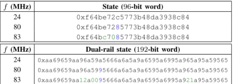
Table IV
STATE AND DUAL-STATE DIFFERENCES AT THE THIRD ROUND.
BLUEMEANS“VALID”ERROR,SUCH AS(0, 1)→(1, 0),WHEREAS
GREENMEANS“SINGLE BIT RESET”ERROR,SUCH AS(0, 1)→(0, 0).
(DATA EXTRACTED FROMFIG.6).
f (MHz) State (96-bit word)
24 0xf64be72c5773b48da3938c84
80 0xf64be7285773b48da3938c84
83 0xf64bc7085773b48da3938c84 f (MHz) Dual-rail state (192-bit word)
24 0xaa69659aa96a59a5666a6a5a9a6595a6995a965a95a59565
80 0xaa69659aa96a5995666a6a5a9a6595a6995a965a95a59565
83 0xaa69659aa12a0095666a6a5a9a6595a6995a921a95a59565
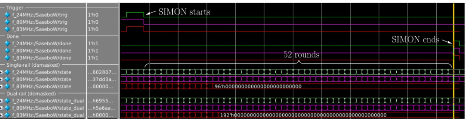
a) Overclocking with fixed plaintext: We increase the
clock frequency of the SIMON block cipher from 24 MHz
until the ciphertext gets erroneous. We choose a
plain-text pt = 0x2072616c6c69702065687420 and a key
k = 0x0d0c0b0a0908050403020100. The resulting
WLF waveforms as dumped by ChipScope are joined, and are represented in Fig.5. Three acquisitions are taken:
1) the first one for f = 24 MHz (in green),
2) the second one for f = 80 MHz (in pink), and
3) the last one for f= 83 MHz (in red).
The correct ciphertext is 0x602807a462b469063d8ff082.
The three computations trigger at the same time. In Fig. 5,
the scale is given round by round (it is not a time scale).
At 80 MHz, we observe in Fig. 5, that a fault is created
in the circuit. We recall that the synthesis report (Tab. III)
announced a maximal frequency of 77 MHz, but the FPGA
still functions normally until < 80 MHz. Nonetheless, at
80 MHz, the computed ciphertext is different from 0: it is 0x37dd3ac20989b9360ebef34a. By carrying on
in-creasing the frequency value of frequency until 83 MHz,
the ciphertext stays at 0x37dd3ac20989b9360ebef34a. Then, over 83 MHz, the ciphertext becomes 0 (as should happen in theory with PC-II netlists).
An explanation why at f = 80 MHz the ciphertext is not
full-zero can be seen by doing a zoom on Fig.5: we find that at the third round, the state starts to be incorrect.
For the reader’s convenience, the state value is also given in Tab. IV. At the round three, the value of the valid state is
0xf64be72c5773b48da3938c84. For f = 80 MHz, the
corrupted state is 0xf64be7285773b48da3938c84. The
nibble c is changed in 8 at the eighth position of the state.
In dual-rail, this corresponds to value a being changed to 9.
Now, a represents (1010)2, namely the two bits (1, 0) and
(1, 0), whereas 9 means (1001)2 in binary, which is a valid
case in LUT6 2 truth table (recall Tab.II). Thus, this exemple illustrates the replacement of a licit value by another one, as in Fig.3(c). So, on the critical path, there exists one LUT6 2 where a pair of dual-rail wires(1, 0) was changed in(0, 1), a valid value in dual-rail. Consequently the SIMON computes with a valid false state and it is possible to attack the circuit thanks to a DFA.
SIMON starts
SIMON ends 52 rounds
Figure 5. One experimental results of SIMON running at 24 MHz, and overclocked at 80 MHz and 83 MHz
Figure 6. Zoom on Fig.5, where we identify the first round (namely round #3) where a fault occurs
For f = 83 MHz, the first error in the state also
oc-curs at third round. There, the faulted state takes the value
0xf64bc7085773b48da3938c84. The nibbles e, 2 and c
at positions respectively 5, 7 and 8 becomec,0and8. In
dual-rail, the numbers 1, 2,0 are encoded in binary as(0001)2,
(0010)2,(0000)2. Those faults are single bit-flips. Thus, faulty states appear, and so a zeroization wave propagates. As can
be seen in Fig. 5, the state reaches the value of zero at the
round 11.
It is noteworthy that fault injections, if successful, can still be exploited despite the implementation is masked. Indeed, irrespective of the masking and the implementation details, a fault propagates until the output. The interested reader is referred to this paper [28] for more details.
b) Overclocking with varying plaintexts: By changing
the plaintext, the clock frequency when the circuit starts to be faulty changes, but remains around 80 MHz. Indeed, it is a well known fact that the critical path is data-dependent.
In Fig. 7, we present the effect of overclocking PC-II with
30 plaintexts. The experiment is performed using 1000 steps
of 0.01 MHz. In total, the DUT frequency is changed from
75 MHz to 85 MHz. The red color in the Fig.7means that no
fault occurred. The blue color means that the PC-II circuit is faulted with a non-zero ciphertext. Eventually, the green color means that the PC-II circuit is faulted with an output fully
Frequency P lai n te x t # 76 77 78 79 80 5 10 15 20 25 30 0 0.5 1 1.5 2 F au lt ed , b u t N o fa u lt Z er oi za ti on n on -z er o Ciphertext: 75 77 79 81 83 85
Figure 7. Effect of overclocking on 30 plaintexts for different frequencies
zeroized. We notice that, there is around 50% (16/30 plaintexts faulted with non-zeroization output) of probability to created an exploitable (not fully zero) fault, in a range of about4 MHz
(that is, between79 and 83 MHz). In the other 50%, the (0, 0)
values generated by the PC-II countermeasure absorb potential harmful(0, 1) ↔ (1, 0) faults. Still, with roughly a probability of1/2, bypassing PC-II is possible provided the fault injection
is controlled precisely enough.
We raised the clock frequency much beyond 85 MHz.
Interestingly, the result remains zeroized for all the bits. One could have imagined that for a high enough frequency, only valid bits from the previous state are sampled. But apparently, there is consistently at least one gate which transitions, hence
with output equal to (0, 0). In the extreme case, the clock
would be so fast that the previous state would be sampled verbatim. But this would have no effect, since the round counter would also stall during this fast clock period. At least, this situation is harmless if the computation path and the control logic are both implemented in PC-II. If only the computation is implemented in PC-II and the logic in regular (faster) logic, then it would be possible to skip [29] or add [30] rounds.
3) Electromagnetic injections: The SIMON 96/96 in
PC-II under EM injections behaves similarly as in the case of overclocking.
D. Discussion
The faults obtained by overclocking and EM injection are similar on our platform. We can deduce that we caused delay faults. When the injected field is very strong, EM injection can also cause sampling faults [31], where the DFFs are perturbed while they sample, precisely by having the EM pulse happen timely with the clock rising edge. Such fault model would not allow correlated faults, hence would not harm private circuits II. But the global timing faults are harmful: it is thus important, for the faults to be exploitable, to exercise only gentle stress: overclocking must have an effect, but not too strong, otherwise too many timing violations occur, amongst them zeroization can occur and wash the licit faulted values. EM injection must not cause DFF malfunctions, only increase the delay in gates, hopefully touching first the critical path.
V. CONCLUSION AND PERSPECTIVES
This paper has shown the possibility to collect erroneous outputs from cryptographic circuits protected by the private circuits II countermeasure, allowing different sorts of attacks, such as the differential fault analysis.
We notice that ChipScope (or equivalently SignalTap in Altera) is a nice tool to investigate the effects of faults on circuits. We leverage on this tool, apparently for the first time, to determine exactly the fault models for overclocking.
As a perspective, we intend to take advantage of the zeroization process to test other attack paths, such as fault sensibility analysis [32] (the stress level at which a fault occurs is data dependent). Let us remark that safe errors are a priori not possible, since in hardware, even values which do not impact the computation value at the logic level are protected. For instance, a multiplexer with the non-selected input at the invalid zero value will propagate an invalid zero value all the same. Obviously, the fault attacks we present applies to other protected circuits, namely dual-rail circuits (WDDL, MDPL, etc.).
Besides, a recent paper [14] has shown similarities between PC-II and threshold implementation, a logic sytle which is the-oretically designed to withstand glicthes. Practical validation would definitely make sense.
ACKNOWLEDGMENTS
The authors a grateful to Laurent Sauvage for setting up the fault injection platform and valuable pieces of advice. We also thank Thibault Porteboeuf for exchanges about ChipScope setup under ISE.
REFERENCES
[1] C. Chen, T. Eisenbarth, A. Shahverdi, and X. Ye, “Balanced Encoding to Mitigate Power Analysis: A Case Study,” in CARDIS, ser. Lecture Notes in Computer Science. Springer, November 2014, paris, France. [2] P. Rauzy, S. Guilley, and Z. Najm, “Formally proved security of assembly code against power analysis,” Journal of Cryptographic Engineering, pp. 1–16, 2015. [Online]. Available: http://dx.doi.org/10. 1007/s13389-015-0105-2
[3] “The Other Side of The Coin: Analyzing Software Encoding Schemes Against Fault Injection Attacks,” in CARDIS, 2015.
[4] Y. Ishai, A. Sahai, and D. Wagner, “Private Circuits: Securing Hardware against Probing Attacks,” in CRYPTO, ser. Lecture Notes in Computer Science, vol. 2729. Springer, August 17–21 2003, pp. 463–481, santa Barbara, California, USA.
[5] Y. Ishai, M. Prabhakaran, A. Sahai, and D. Wagner, “Private Circuits II: Keeping Secrets in Tamperable Circuits,” in EUROCRYPT, ser. Lecture Notes in Computer Science, vol. 4004. Springer, May 28 – June 1 2006, pp. 308–327, St. Petersburg, Russia.
[6] S. Mangard, E. Oswald, and T. Popp, Power Analysis Attacks: Revealing the Secrets of Smart Cards. Springer, December 2006, ISBN 0-387-30857-1,http://www.dpabook.org/.
[7] C. Helfmeier, D. Nedospasov, C. Tarnovsky, J. S. Krissler, C. Boit, and J.-P. Seifert, “Breaking and entering through the silicon,” in ACM Conference on Computer and Communications Security, A. Sadeghi, V. D. Gligor, and M. Yung, Eds. ACM, 2013, pp. 733–744. [Online]. Available:http://dl.acm.org/citation.cfm?id=2508859
[8] M. Gomathisankaran and A. Tyagi, “Glitch resistant private circuits design using HORNS,” in IEEE Computer Society Annual Symposium on VLSI, ISVLSI 2014, Tampa, FL, USA, July 9-11, 2014, 2014, pp. 522–527. [Online]. Available:http://dx.doi.org/10.1109/ISVLSI.2014.93
[9] Y. Yu, J. Leiwo, and B. Premkumar, “Private stateful circuits secure against probing attacks,” in ASIACCS. ACM, March 20-22 2007, pp. 63–69, Singapore.
[10] J. Park and A. Tyagi, “t-Private logic synthesis on FPGAs,” in Hardware-Oriented Security and Trust (HOST), 2012 IEEE Interna-tional Symposium on, June 2012, pp. 63–68.
[11] ——, “t-Private Systems: Unified Private Memories and Computation,” in Security, Privacy, and Applied Cryptography Engineering, ser. Lecture Notes in Computer Science, R. Chakraborty, V. Matyas, and P. Schaumont, Eds., vol. 8804. Springer International Publishing, 2014, pp. 285–302. [Online]. Available: http://dx.doi.org/10.1007/ 978-3-319-12060-7 19
[12] ——, “Towards making private circuits practical: DPA resistant private circuits,” in IEEE Computer Society Annual Symposium on VLSI, ISVLSI 2014, Tampa, FL, USA, July 9-11, 2014, 2014, pp. 528–533. [Online]. Available:http://dx.doi.org/10.1109/ISVLSI.2014.24
[13] S. Nikova, C. Rechberger, and V. Rijmen, “Threshold Implementations Against Side-Channel Attacks and Glitches,” in ICICS, ser. LNCS, vol. 4307. Springer, December 4-7 2006, pp. 529–545, Raleigh, NC, USA. [14] O. Reparaz, B. Bilgin, S. Nikova, B. Gierlichs, and I. Verbauwhede, “Consolidating Masking Schemes,” in Advances in Cryptology -CRYPTO 2015 - 35th Annual Cryptology Conference, Santa Barbara, CA, USA, August 16-20, 2015, Proceedings, Part I, ser. Lecture Notes in Computer Science, R. Gennaro and M. Robshaw, Eds., vol. 9215. Springer, 2015, pp. 764–783. [Online]. Available:
http://dx.doi.org/10.1007/978-3-662-47989-6 37
[15] M. Rivain and E. Prouff, “Provably Secure Higher-Order Masking of AES,” in CHES, ser. LNCS, S. Mangard and F.-X. Standaert, Eds., vol. 6225. Springer, 2010, pp. 413–427.
[16] H. Kim, S. Hong, and J. Lim, “A Fast and Provably Secure Higher-Order Masking of AES S-Box,” in CHES, ser. LNCS, B. Preneel and T. Takagi, Eds., vol. 6917. Springer, 2011, pp. 95–107.
[17] J. Coron, J. Großsch¨adl, and P. K. Vadnala, “Secure Conversion between Boolean and Arithmetic Masking of Any Order,” in Cryptographic Hardware and Embedded Systems - CHES 2014 - 16th International Workshop, Busan, South Korea, September 23-26, 2014. Proceedings, ser. Lecture Notes in Computer Science, L. Batina and M. Robshaw, Eds., vol. 8731. Springer, 2014, pp. 188–205. [Online]. Available:
http://dx.doi.org/10.1007/978-3-662-44709-3 11
[18] J.-L. Danger, S. Guilley, and F. Flament, “Procede de detection d’anomalies dans un circuit de cryptographie protege par logique differentielle et circuit mettant en oeuvre un tel procede,” Feb. 8 2012, eP Patent 2,324,442. [Online]. Available:http://www.google.com/ patents/EP2324442B1?cl=zh
[19] Xilinx, “Virtex-6 Libraries Guide for HDL Designs (UG623, v 13.1),” p. 239, March 1 2011, Primitive: Six-input, 2-output, Look-Up Table, http://www.xilinx.com/support/documentation/sw manuals/
xilinx13 1/virtex6 hdl.pdf.
[20] S. Bhasin, S. Guilley, F. Flament, N. Selmane, and J.-L. Danger, “Countering Early Evaluation: An Approach Towards Robust Dual-Rail Precharge Logic,” in WESS. ACM, October 24-28 2010, pp. 6:1–6:8, Scottsdale, Arizona, USA. DOI: 10.1145/1873548.1873554.
[21] R. Beaulieu, D. Shors, J. Smith, S. Treatman-Clark, B. Weeks, and L. Wingers, “The SIMON and SPECK Families of Lightweight Block Ciphers,” Cryptology ePrint Archive, Report 2013/404, 2013, http:
//eprint.iacr.org/2013/404.
[22] S. Bhasin, T. Graba, J. Danger, and Z. Najm, “A look into SIMON from a side-channel perspective,” in 2014 IEEE International Symposium on Hardware-Oriented Security and Trust, HOST 2014, Arlington, VA, USA, May 6-7, 2014. IEEE Computer Society, 2014, pp. 56–59. [Online]. Available:http://dx.doi.org/10.1109/HST.2014.6855568
[23] L. Sauvage, M. Nassar, S. Guilley, F. Flament, J.-L. Danger, and Y. Mathieu, “Exploiting Dual-Output Programmable Blocks to Balance Secure Dual-Rail Logics,” International Journal of Reconfigurable Com-puting (IJRC), p. 12, 2010, DOI: 10.1155/2010/375245.
[24] W. He, A. Otero, E. de la Torre, and T. Riesgo, “Customized and Automated Routing Repair Toolset Towards Side-Channel Analysis Resistant Dual Rail Logic,” Microprocessors and Microsystems, 2014, DOI: 10.1016/j.micpro.2014.02.005.
[25] A. Moradi and V. Immler, “Early Propagation and Imbalanced Routing, How to Diminish in FPGAs,” in Cryptographic Hardware and Embedded Systems - CHES 2014 - 16th International Workshop, Busan, South Korea, September 23-26, 2014. Proceedings, ser. Lecture Notes in Computer Science, L. Batina and M. Robshaw, Eds., vol. 8731. Springer, 2014, pp. 598–615. [Online]. Available:
http://dx.doi.org/10.1007/978-3-662-44709-3 33
[26] G. Piret and J.-J. Quisquater, “A Differential Fault Attack Technique against SPN Structures, with Application to the AES and KHAZAD,” in CHES, ser. LNCS, vol. 2779. Springer, September 2003, pp. 77–88, Cologne, Germany.
[27] N. Selmane, S. Guilley, and J.-L. Danger, “Setup Time Violation Attacks on AES,” in EDCC, The seventh European Dependable Computing Conference, Kaunas, Lithuania, May 7-9 2008, pp. 91–96, ISBN: 978-0-7695-3138-0, DOI: 10.1109/EDCC-7.2008.11.
[28] A. Boscher and H. Handschuh, “Masking Does Not Protect Against Differential Fault Attacks,” in FDTC, 5th Workshop on Fault Detection and Tolerance in Cryptography, IEEE-CS, aug 2008, pp. 35–40, DOI: 10.1109/FDTC.2008.12, Washington, DC, USA.
[29] Y. Monnet, M. Renaudin, R. Leveugle, C. Clavier, and P. Moitrel, “Case Study of a Fault Attack on Asynchronous DES Crypto-Processors,” in FDTC, ser. Lecture Notes in Computer Science, vol. 4236. Springer, October 10 2006, pp. 88–97, Yokohama, Japan.
[30] A. Dehbaoui, A.-P. Mirbaha, N. Moro, J.-M. Dutertre, and A. Tria, “Electromagnetic glitch on the aes round counter,” in Constructive Side-Channel Analysis and Secure Design, ser. Lecture Notes in Computer Science, E. Prouff, Ed. Springer Berlin Heidelberg, 2013, vol. 7864, pp. 17–31. [Online]. Available: http://dx.doi.org/10.1007/ 978-3-642-40026-1 2
[31] S. Ordas, L. Guillaume-Sage, K. Tobich, J. Dutertre, and P. Maurine, “Evidence of a Larger EM-Induced Fault Model,” in CARDIS 2014, Paris, France, November 5-7, 2014. Revised Selected Papers, ser. Lecture Notes in Computer Science, M. Joye and A. Moradi,
Eds., vol. 8968. Springer, 2014, pp. 245–259. [Online]. Available:
http://dx.doi.org/10.1007/978-3-319-16763-3 15
[32] Y. Li, K. Sakiyama, S. Gomisawa, T. Fukunaga, J. Takahashi, and K. Ohta, “Fault Sensitivity Analysis,” in CHES, ser. Lecture Notes in Computer Science, vol. 6225. Springer, August 17-20 2010, pp. 320– 334, Santa Barbara, CA, USA.
[33] L. Batina and M. Robshaw, Eds., Cryptographic Hardware and Embedded Systems - CHES 2014 - 16th International Workshop, Busan, South Korea, September 23-26, 2014. Proceedings, ser. Lecture Notes in Computer Science, vol. 8731. Springer, 2014. [Online]. Available: