HAL Id: hal-01879162
https://hal.archives-ouvertes.fr/hal-01879162
Submitted on 22 Sep 2018
HAL is a multi-disciplinary open access
archive for the deposit and dissemination of sci-entific research documents, whether they are pub-lished or not. The documents may come from teaching and research institutions in France or abroad, or from public or private research centers.
L’archive ouverte pluridisciplinaire HAL, est destinée au dépôt et à la diffusion de documents scientifiques de niveau recherche, publiés ou non, émanant des établissements d’enseignement et de recherche français ou étrangers, des laboratoires publics ou privés.
Liquid crystal-based tunable photodetector operating in
the telecom C-band
Christophe Levallois, Benattou Sadani, Benjamin Boisnard, Thierry Camps,
Cyril Paranthoen, Salvatore Pes, Sophie Bouchoule, Laurent Dupont,
Jean-Baptiste Doucet, Mehdi Alouini, et al.
To cite this version:
Christophe Levallois, Benattou Sadani, Benjamin Boisnard, Thierry Camps, Cyril Paranthoen, et al.. Liquid crystal-based tunable photodetector operating in the telecom C-band. Optics Express, Optical Society of America - OSA Publishing, 2018, 26 (20), pp.25952-25961. �10.1364/OE.26.025952�. �hal-01879162�
Liquid crystal-based tunable photodetector
operating in the telecom C-band
C
HRISTOPHEL
EVALLOIS,
1,*B
ENATTOUS
ADANI,
2B
ENJAMINB
OISNARD,
2T
HIERRYC
AMPS,
2C
YRILP
ARANTHOËN,
1S
ALVATOREP
ES,
1S
OPHIEB
OUCHOULE,
3L
AURENTD
UPONT,
4J
EAN-B
APTISTED
OUCET,
2M
EHDIA
LOUINI,
1ANDV
ÉRONIQUEB
ARDINAL21Univ Rennes, INSA Rennes, CNRS, Institut FOTON – UMR 6082, F-35000 Rennes, France 2Univ Toulouse, CNRS, LAAS, 7 Avenue Colonel Roche, F-31400 Toulouse, France
3Centre de Nanosciences et de Nanotechnologies, CNRS, Université Paris-Sud, 91360 Marcoussis,
France
4IMT Atlantique, Optics Department, 655 Avenue du Technopôle, 29200 Plouzané, France *[email protected]
Abstract: Liquid crystal (LC) microcells monolithically integrated on the surface of InGaAs
based photodiodes (PDs) are demonstrated. These LC microcells acting as tunable Fabry-Perot filters exhibit a wavelength tunability of more than 100 nm around 1550 nm with less than 10V applied voltage. Using a tunable laser operating in the S and C bands, photocurrent measurements are performed. On a 70 nm tuning range covered with a driving voltage lower than 7V, the average sensitivity for the PD is 0.4 A/W and the spectral linewidth of the LC filter remains constant, showing a FWHM of 1.5 nm. Finally, the emission spectrum from an Er-doped fiber is acquired by using this tunable PD as a micro-spectrometer.
© 2018 Optical Society of America under the terms of the OSA Open Access Publishing Agreement
1. Introduction
Compact photonic devices with wavelength tuning capability are of great interest for optical communication or metrology applications. Beyond the advantages related to integrated aspect, low power consumption, robustness and low production costs are important factors to make such tunable components attractive. Reconfigurable wavelength selective photodetectors (PDs) are highly interesting for optical communication systems. Such devices can also find interest as a compact and reconfigurable optical sensor, as a micro-spectrometer [1,2], or as a wavelength-meter completely integrated on a chip [3].
Tunable photonic devices have been a subject of intense studies for the last two decades, mainly focusing on tunable optical sources such as VCSELs [4]. However, studies have also been conducted on tunable PDs [5–13]. As for VCSELs, tunable PDs have been mainly developed by using MEMS technologies. In this case, the physical length of a resonant microcavity is varied with an electrostatically or thermally actuated movable mirror. Different approaches are commonly exploited for the realization of MEMS-PD, with the use of a Resonant-Cavity-Enhanced design where absorbing layers are inserted inside the microcavity [3,5], or with the simple assembly of a PD with a wavelength resonant MEMS filter [6,7]. Recently, a promising MEMS-PD has been reported, with the demonstration of a 180 nm tuning range around 1.55 µm [8]. However, thermally actuated MEMS solutions may have some drawbacks related to slow tuning speed and power consumption. In the case of electrostatic actuation, a high driving voltage can be also required. Thus, alternative approaches to MEMS have been investigated as well. The use of quantum confined Stark effect (QCSE) can be cited for a PD integrating multi-quantum wells as absorbing material [9,10]. Also, monolithic approaches with resonant microcavities tuned by thermal-optic effect and directly bonded or grown on PD arrays were reported [11,12]. However, the major drawback remains the achievable tuning range, limited around ten nanometers for QCSE or monolithic approaches, and a poor spectral selectivity in the case of QCSE. Obviously, the
tuning range can be increased by combining several tunable PDs [13], but that leads to a more complex design and a more expensive device.
A promising alternative to all these approaches is the use of liquid crystal (LC) which can provide a large refractive index tuning with a moderate driving voltage and very low power consumption. Passive and macroscopic devices consisting in a LC-based tunable Fabry-Perot (FP) filter have been demonstrated for a long time [14,15]. More recently, compact photonic devices combining active components such as lasers [16] or VCSEL [17,18] with LC material have been demonstrated. In this case, the operating wavelength of the laser or its polarization state can be tuned. LC layers have also been used in passive components to obtain for example wavelength-tunable ring resonators integrated on silicon-on-insulator substrate [19]. In contrast, an attempt to use LC-based tunable FP filter with a photodetection system for spectral imaging application has been also demonstrated, however it was done within a macroscopic optical set-up [20]. Thus, the combination of LC monolithically integrated with micron-sized devices to obtain wavelength-selective PDs has never been demonstrated. In this work, we report for the first time InGaAs-based PDs integrating LC-microcells resonant cavities on their surfaces, which act as a wavelength-selective filter for the PDs. Characterization of the tunable filter and photocurrent measurements are presented and discussed. Finally, a LC tunable PD is turned into microspectrometer whose operation in the telecom C-band is illustrated on an Er-doped optical fiber.
2. Device design and fabrication
2.1 Principle of the tunable PD
Our tunable PD consists in micro-sized LC based FP filters monolithically integrated above standard InGaAs photodiodes arrays (see Fig. 1). For such a filter, the average orientation of the LC molecules (i.e. the director) can be electrically controlled to change the effective refractive index of the FP resonator, enabling a shift in the resonant wavelength which can be detected by the PD. However, to benefit from a large refractive index variation and then a large tuning range, it is mandatory to control the director by using a LC alignment film (see section 2.3 for details about this alignment film). Thus, an incident light with a linear polarization parallel to the director experiences the refractive index change if a voltage is applied on the LC. As illustrated in Fig. 1(e), when no voltage is applied on the cell, the director is parallel to the surface, and the refractive index is maximum (close to the extraordinary index, ne). As the applied voltage increases, the director is reoriented and the
refractive index decreases towards n0 (the ordinary index) leading in a blue shift for the
resonant wavelength with a polarization parallel to the director. The resonant mode with a linear polarization parallel (or perpendicular) to the director will be referred to as “extraordinary mode” (or “ordinary mode”) in the following. As already pointed out, such an approach has numerous advantages in comparison with MEMS solution: no moving parts, a moderate driving voltage and low power consumption. However, LC material may have limitations. Indeed, nematic LC is a birefringent material, and as a consequence the tunable FP filter will be sensitive to the polarization of the incident light. Therefore, our PD must be correctly oriented (polarization along the director) for an optimal detection of the light. For unpolarized light, the PD can still be used but its responsivity will be reduced, and possibly a higher dark current could exist if the ordinary modes are detected. Another point is the LC response times which are expected to be in the millisecond range. This is slower than MEMS electrostatically driven, but comparable to, if not lower than, MEMS electro-thermally actuated [4].
2.2 PD fabrication
The semiconductor part of the PD was grown by molecular beam epitaxy on a 2 inch (001)-oriented InP substrate. The epitaxial layers of the PIN structure consist of a 200 nm InP
n-type buffer layer, a 1 µm undoped In0.53Ga0.47As absorption layer and a 200 nm p-type
In0.53Ga0.47As contact layer. This PIN structure is then processed to define arrays of circular or
square PDs with photosensitive areas ranging from 0.01 mm2 to 0.3 mm2. Figure 1(a)
illustrates a quarter of the InP substrate at the end of the PD process, when Fig. 1(d) gives a 3D view of a single tunable PD. To fabricate these PDs, first, a dry etching of In0.53Ga0.47As
layers down to the n-type InP contact layer is done to form mesas providing electrical insulation between the different PD. Second, a 200 nm PECVD layer of SiNx is deposited and
etched to define electrical contact apertures at the surface of each mesa. Third, a 20 nm Ti and a 500 nm Au layers are evaporated and patterned by a liftoff process to form the top p-type contact when bottom n-type contact is ensured by the deposition of a 300 nm AuGe layer on the backside of the InP wafer.
Fig. 1. Images of the tunable PD sample at different steps of the fabrication process (a) after PD fabrication, (b) after deposition of the aSi/SiNx bottom DBR, (c) at the end of the process.
(d) 3D and cross-section view for a single tunable PD. (e) Schematic view of the LC molecules reorientation with AC voltage applied to LC microcells.
2.3 Tunable filter fabrication
The technological process then continues with the collective fabrication of microscopic LC cells monolithically integrated which act as tunable filters to operate the device as a selective-wavelength PD. First, a bottom distributed Bragg reflector (DBR), consisting in 2.5 periods of amorphous silicon (a-Si) and SiNx is deposited by magnetron sputtering on the PD sample.
These layers are added to the quarter-wave SiNx layer already deposited by PECVD to form a
DBR of 3 periods with a theoretical reflectivity of 97%. Such a DBR has been chosen as bottom mirror since its deposition and etching are well controlled and have already been used within other types of III-V devices [21]. This DBR is then etched on the edges of the sample to keep an electrical access to the different PDs (see Fig. 1(b)). Note that for the clarity of Fig. 1(d), layers of the bottom DBR have been drawn only on the photosensitive area of the PD, even if these layers cover the main part of the sample, as shown in Fig. 1(b). Then, on this bottom DBR, the surface has to be prepared for the following filling of LC microcells while ensuring the director orientation. Usually, for large and flat LCD display surfaces, this is done by a polyimide surface rubbing, which is a well-known and effective method. However, this approach is not compatible with a micro-scale device process, especially when a non-planar
surface topography exists. Nevertheless, LC alignment can be also obtained through a planar anchoring on a surface relief grating. In our fabrication process, this has been done by imprinting a sub-wavelength grating mold in a 700 nm thick SU-8 layer previously spin-coated on the bottom DBR surface. Details about this process can be found elsewhere [22]. As for the bottom DBR, the nanoimprinted SU-8 layer has been drawn only on the photosensitive area of the PD in the Fig. 1(d). The sub-wavelength grating is well transferred onto SU-8 layer with a period of 800 nm, a duty cycle of 50:50, and a depth in the range of [70-80 nm]. Such grating has been designed in such a way it allows an efficient orientation of the LC molecules during the filling of LC microcells, as well as limiting diffraction optical losses at 1.55 µm working wavelength. LC microcells are then defined by polymer walls made of an epoxy photosensitive film named DF-1005. The advantage in the use of this polymer is related to its form, a dry resist film of 5 µm in thickness that can be applied directly to the sample surface by a soft thermal transfer [23]. This leads to a high homogeneity in the thickness of the polymer film, especially for small dimensions samples for which proper spin-coating of thick polymer layers is a difficult task considering the uniformity constraint in designing a microcavity. The DF-1005 walls are then defined by standard photolithography steps to form several square areas of 3.5 × 3.5 mm2 which are each
composed of arrays of 9 PDs, as shown in Fig. 1(c). These microcells are then covered by a top DBR with a theoretical reflectivity of 95%, consisting of 5 x (SiO2/TiO2) periods
deposited on a glass substrate, previously coated with a 23 nm ITO electrode having a sheet resistance of 100 Ω/2/TiO2) Bragg pairs has been designed to
maximize the transmission into the PD at the LC micro-filter resonance wavelength (Tmax-theo
~80%). This upper part of the device, covered by an antireflection TiO2/SiO2 bi-layer at 1.55
µm, is then sealed to the top surfaces of the DF walls. The sealing is performed using 700 nm thick SU-8 layer spin-coated on the top DBR followed by a UV exposure through the-SiO2/TiO2 DBR which is UV-transparent, unlike the aSi/SiNx DBR which cannot be used as a
top mirror here. The final step consists in filling under vacuum the microcells by a typical nematic LC (E7). This filling is achieved at a temperature higher than the nematic-isotropic transition (i.e. >70 °C) thanks to lateral apertures previously defined in the DF-1005 cells’walls.
3. Results and discussion
3.1 Tunable filter characterization
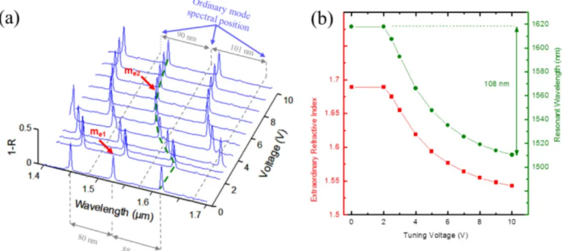
Prior to the characterization of the device as a wavelength selective PD, polarization-resolved reflectivity measurements of the tunable filter were performed by a Fourier transform infra-red spectrometer (FTIR). Figure 2(a) shows the spectra recorded for an applied AC voltage at 2 kHz and different amplitudes comprised between 0 and 10V. The voltage is applied through the ITO and AuGe electrodes. These measurements were performed above the photosensitive area of a PD (380 × 380 μm2) which is larger than the area analyzed by the FTIR (150 × 150
μm2). Figure 2(a) gives an overview of the extraordinary modes. The ordinary modes are not
visible since the incident light polarization is oriented along the gratings lines. Nevertheless, their spectral positions are indicated for information, as well as the corresponding values of free spectral ranges between successive modes (FSR). Obviously, this FSR parameter is an important parameter that can be increased by a thickness reduction of the LC layer. However, a compromise must be made between the FSR and the width of the tuning range which also depends on the LC thickness. Indeed, a too thick LC layer would induce a large tuning range but also a too large crossing number between the different modes of the FP resonator, limiting the operation of the PD.
Fig. 2. (a) Evolution of reflectivity spectra (plotted as 1-R for improved clarity) measured by localized FTIR spectroscopy on a PD area for different AC voltages (2 kHz) varying from 0 to 10V in amplitude. The orientation of the polarizer was chosen to attenuate the “ordinary” modes. (b) Resonant wavelength shift of extraordinary modes and deduced refractive index variation as a function of the applied tuning voltage on the LC filter.
When a voltage is applied, the extraordinary modes are shifted towards shorter wavelengths, which is consistent with the fact that ne decreases when the electric field is
increased. This resonance wavelength shift starts at a threshold voltage of 2.5V. The spectral differences between ordinary and extraordinary modes have been studied by modeling the structure reflectivity using the transfer matrix method (TMM). The 90 and 101 nm spacings between the ordinary modes are correctly reproduced considering a LC thickness of 6.4 μm. This thickness turned out to be higher than the expected one, i.e. higher than the nominal thickness of the DF walls. This result can be explained by a SU-8 layer spin-coated on the bottom DBR thicker than expected, presumably due to the non-planar topography of the InP sample after PD process. Thus, the local extra thicknesses of this SU-8 layer led to a resulting thickness for the LC microcells higher than the DF walls thickness. By tracking the extraordinary modes wavelength position, the refractive index variation as a function of the applied voltage can be deduced (red curve in Fig. 2(b)) with the TMM confrontation. The value deduced for ne is 1.689, i.e. close to that already measured for this type of LC at 25 °C
(ne = 1.697) [14,22], confirming that the alignment of the LC molecules along the grating
lines is efficient. The linear dependence between the refractive index and the resonant wavelength leads to similar variation behaviors for the shift of the resonant wavelength as a function of the applied LC voltage (green curve in Fig. 2(b)). For this extraordinary mode, a wavelength shift of 108 nm, higher than the FSR (88 nm), is demonstrated with a maximum applied voltage of only 10V. Note that the filter spectral width is overestimated in this experiment due to the high numerical aperture of the microscope objective used for focusing. It will be assessed later
3.2 Tunable PD characterization
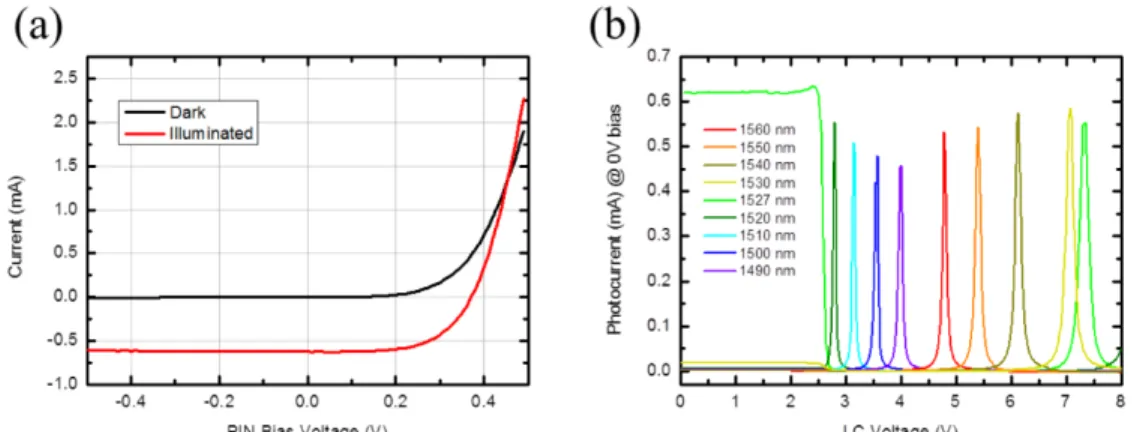
Photocurrent measurements were undertaken using a tunable external cavity laser, delivering a continuous mode-hop-free tuning over 80 nm [1480 nm - 1560 nm] with a 5 MHz FWHM. The laser beam was focused with a lens of 40 mm focal length to form on the PD a spot with a diameter of 100 µm, smaller than any PD area on the sample. Figure 3 shows the I-V curves without any LC voltage and photocurrent detected as a function of the LC voltage for a square PD (380 × 380 μm2) including the tunable filter whose characteristics have been described
Fig. 3. (a) I-V curves in the dark and under 1.4 mW illumination at 1527 nm for a 380 × 380 µm2 PD without any LC voltage. (b) Photocurrent for the same PD related to resonant
extraordinary modes vs AC voltage (2 kHz) applied on the LC microcell for different lasing wavelengths fixed at an input power of 1.4 mW.
As it can be seen in Fig. 3(a) where the excitation wavelength at 1527 nm is resonant with the LC filter, a photocurrent higher than 0.6 mA is detected without any LC voltage and when the PD is illuminated with an incident power of 1.4 mW. In the following, we have fixed the PD bias at 0V and measured the photocurrent amplitude as function of the applied LC voltage, and for different laser incident wavelengths (See Fig. 3(b)). For the starting wavelength of 1527 nm, the photocurrent is almost constant at 0.62 mA over the LC voltage range [0V - 2V], then it falls to almost the dark current value (around 1µA) from 2.5V to 7V, and finally presents a peak for a voltage of 7.5V. As shown previously in Fig. 2(a), the LC extraordinary index remains constant over the [0V - 2V] range, meaning that this high value of photocurrent corresponds to a perfect match of the filter with the lasing wavelength of 1527 nm, as indicated with the arrow labelled me1 on Fig. 2(a). The photocurrent peak at 7.5
V is related to the shift of the adjacent extraordinary mode previously measured by FTIR, initially located above 1600 nm (see Fig. 2 (a), arrow labelled me2), and found at 1527 nm for
a LC voltage around 7V. As shown in Fig. 3(b), these measurements were performed for several wavelengths. For each wavelength, a photocurrent peak was detected for a particular LC voltage remaining below 7V, clearly demonstrating that this PD operates as a wavelength-selective PD over the whole available spectral characterization range (80 nm).
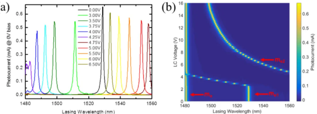
As real transmittance and linewidth measurements of the FP filter were not possible with our FTIR set-up, other photocurrent measurements were undertaken to evaluate these parameters which are mainly related to the reflectivity of the DBR and to internal optical losses of the FP resonator. First, in order to evaluate the quality factor (Q-factor) of the whole tunable PD, photocurrent measurements with a continuous sweep on the incident laser wavelength and at a fixed LC voltage were also performed (see Fig. 4(a)). Figure 4(b) presents the same measurements, but plotted under the form of LC voltage/wavelength mapping and where the photocurrent value is given as a color scale. On this figure, the vertical line at 1482 nm labelled m0 represents the photocurrent variation of the ordinary
mode as function of LC voltage. To perform this measurement, the laser polarization was rotated by 90° relatively with the LC alignment grating. When the polarization of the laser is aligned along the grating, the wavelength shift of photocurrent peaks related to extraordinary modes can be observed. In particular, the two different modes me1 and me2, already identified
in Fig. 2(a), can be seen here in Fig. 4(b). In Fig. 4(a) and 4(b), no significant variation in the photocurrent amplitude is observed, except at a LC voltage of 4.25V. The same observation can be done about the FWHM which can be extracted from Fig. 4(a). The average FWHM of photocurrent peaks is found to be equal to 1.5 nm, except for wavelengths close to 1480 nm, where a coupling between the ordinary and extraordinary modes occurs, leading to degrade
the Q-factor and to decrease the photocurrent values for these specific wavelengths. Thus, if the spectral range from 1480 to 1490 nm is excluded, the Q-factor of the cavity is around 103,
in agreement with the expected value calculated by TMM (Q-calculated≈1 100 in the 1500 nm –
1600 nm range), confirming that the LC absorption for wavelengths around 1.55 μm is negligible [24]. In our case, this also confirms that the intra-cavity nanostructured SU-8 layer does not induce diffraction losses as previously mentioned. This was also verified in a previous work by the authors showing the low losses induced by the SU-8 grating and how this grating is efficient to properly align LC molecules [22].
Fig. 4. (a) Photocurrent spectra of the resonant extraordinary modes measured for different AC voltage applied on the LC microcell as a function of the incident laser wavelength. (b) Photocurrent color mapping for ordinary (m0) and extraordinary modes (me1 and me2) as a
function of the lasing wavelength of the tunable laser and AC voltage applied on LC microcells.
Regarding the responsivity, which is a key parameter for a PD, our results show that over a wide spectral range [1490 nm - 1560 nm], the tunable PD provides photocurrent values comprised between 0.5 and 0.65 mA. Considering the incident input power of 1.4 mW, this leads to a responsivity of 0.35 to 0.46 A/W for the whole device. A comparison with a reference PD was also made at the end of the PD process to evaluate the influence of the filter insertion on the device responsivity. In this case, the SiNx PECVD layer deposited on the
surface of the PD arrays plays the role of an antireflection coating to maximize the light absorbed by the PDs. The measured responsivities for these reference PDs are from 0.57 to 0.64 A/W in the same spectral range, which is consistent with values expected for such PDs integrating only a 1 µm thick In0.53Ga0.47As absorbing layer. In an improved design,
responsivities close to 0.8 and up to 1 A/W could be obtained with such tunable PDs by simply doubling the thickness of the absorbing layer [8]. Finally, the losses related to the integration of the tunable filter on the PD are estimated to be around 2 dB. As already mentioned above, these losses are not related to absorption from any materials within the microcavity. These 2 dB losses are mainly related to the maximal transmission of the filter at the resonance, which is estimated to be around 80% due to a slight reflectivity mismatch between bottom DBR (97%) and top DBR (95%), and to residual absorption within the ITO layers located outside the microcavity.
3.3 Tunable PD as a micro-spectrometer
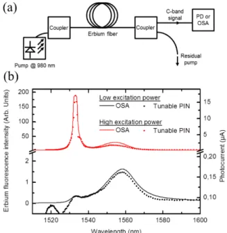
Knowing the experimental relationship between the resonant wavelength of the filter and the LC voltage, the final characterization of the PD consisted in testing it as a micro-spectrometer. The source under consideration was a 20 m Er-doped fiber pumped by a laser diode operating at 980 nm. The residual pump signal was filtered at the fiber output to avoid any detection by the PD (see Fig. 5(a)). The amplified spontaneous emission of this Er-doped fiber lies in the C-band [1530 nm −1565 nm] and is unpolarized. Consequently, this source
can be detected only inside a spectral window delimited by the two successive ordinary modes located at 1482 nm and 1572 nm respectively (see Fig. 2(a)). Thus, it is ensured that the ordinary modes do not come into play. Figure 5(b) shows the spectra recorded for two different excitation power levels of the Er-fiber. The photocurrent spectra obtained were compared with those measured with a commercial optical spectrum analyzer (OSA).
Fig. 5. (a) Scheme of the experimental set-up to test the tunable PD as a micro-spectrometer. (b) Spontaneous emission spectra emitted from an Er-doped fiber excited at two different power levels. The spectra were recorded by the tunable PD and compared with measurements acquired by an optical spectrum analyzer (OSA).
A good agreement between both measurement methods was obtained, demonstrating that this tunable PD can be efficiently used as a micro-spectrometer in the C-band. This result has been obtained without taking into account the slight dependence of the responsivity with the wavelength, but baselines related to the dark photocurrent have been subtracted from the raw photocurrent curves. Future improvements and optimizations in the technological process are under study with the aim to reduce the intra-cavity thicknesses (SU-8 and LC layers). This could lead to a significant increase in the FSR to benefit from a micro-spectrometer with a tuning range higher than 200 nm without crossing between ordinary and extraordinary modes.
4. Conclusion
In this work, we demonstrate tunable PDs consisting in LC microcells integrated on the surfaces of InGaAs PD and acting as resonant microcavities. The tunable part of this device has been characterized by polarization-resolved reflectivity measurements with a FTIR spectrometer. A wavelength tuning higher than 100 nm at 1550 nm with a maximum driving voltage of 10V is achieved. Photodetection measurements were also performed thanks to a tunable laser operating in the S and C bands, demonstrating that the PD is spectrally-tunable and can be swept from 1480 nm to 1560 nm. This spectral window was covered with a LC driving voltage of 7V only. The average responsivity over the major part of this spectral range is measured to be 0.4 A/W, corresponding to less than 2 dB of insertion loss. Q-factor of 103
and spectral linewidth of 0.15 nm have been measured, remaining almost constant over the considered spectral window [1490 nm - 1560 nm]. Finally, as a first applicative demonstration, this tunable PD has been successfully used as a micro-spectrometer to
measure the spontaneous emission emitted by an Er-doped fiber. Presented results consist in the really first demonstration of the integration at a microscale level of LC-based tunable PD, with already satisfying performances considering the needs in miniature spectroscopy applications. Nevertheless, several major improvements can be easily achieved, to increase the tunable PD responsivity by increasing the thickness of the absorbing layer, to increase the wavelength sensitivity by increasing the Q-factor value of the cavity, and also to increase the wavelength tunability span to 200 nm by increasing the FSR of the filter. Considering these improvements, LC based approaches may become a relevant technology for tunable photodetectors in the visible and infrared wavelength range, especially if we consider that the presented technology can be easily adapted to any type of PDs. In addition, as the optical losses induced by LC are negligible, it may also be possible to consider using these LC microcells into a laser cavity to develop tunable emitters.
Funding
Agence Nationale de la Recherche (ANR) and Direction Générale de l'Armement (DGA) (ANR-ASTRID HYPOCAMP, grant ANR-14-ASTR-0007-01); DGA-MRIS and Région Bretagne (grant ARED-VELOCE 8917) and grant ANR-15-CE19-0012 DOCT VCSEL.
Acknowledgments
The authors acknowledge RENATECH (French Network of Major Technology Centers) for technological support. The tunable LC-PD technology was developed at LAAS, Nanorennes, and C2N (in collaboration with IMT Atlantique). The authors also acknowledge X. Lafosse from C2N for his technical support, R.-M. Sauvage (DGA/DS/MRIS) and H. Folliot (Institut FOTON) for fruitful discussions.
References
1. R. F. Wolffenbuttel, “MEMS-based optical mini- and microspectrometers for the visible and infrared spectral range,” J. Micromech. Microeng. 15(7), S145–S152 (2005).
2. L. P. Schuler, J. S. Milne, J. M. Dell, and L. Faraone, “MEMS-based microspectrometer technologies for NIR and MIR wavelengths,” J. Phys. D Appl. Phys. 42(13), 133001 (2009).
3. M. S. Wu, E. C. Vail, G. S. Li, W. Yuen, and C. J. Chang-Hasnain, “Widely and continuously tunable
micromachined resonant cavity detector with wavelength tracking,” IEEE Photonics Technol. Lett. 8(1), 98–100 (1996).
4. P. Qiao, K. Cook, K. Li, and C. J. Chang-Hasnain, “Wavelength-swept VCSELs,” IEEE J. Sel. Top. Quantum Electron. 23(6), 1700516 (2017).
5. G. L. Christenson, A. T. T. D. Tran, Z. H. Zhu, Y. H. Lo, M. Hong, J. P. Mannaerts, and R. Bhat, “Long-wavelength resonant vertical-cavity LED/photodetector with a 75-nm tuning range,” IEEE Photonics Technol. Lett. 9(6), 725–727 (1997).
6. D. Zhou, M. Garrigues, J. L. Leclercq, J. Peng, and P. Viktorovitch, “A phase-matching and pseudoresonance-enhanced design for tunable micromachined photodetectors,” IEEE Photonics Technol. Lett. 15(10), 1443–1445 (2003).
7. H. Halbritter, F. Riemenschneider, S. Syguda, C. Dhanavantri, M. Strassner, A. Tarraf, B. R. Singh, I. Sagnes, and P. Meissner, “Tunable and wavelength selective PIN photodiode,” Electron. Lett. 40(6), 388–390 (2004). 8. J. Cesar, S. Paul, M. T. Haidar, B. Corbett, A. Chipouline, and F. Küppers, “Surface micromachined
MEMS-tunable PIN-photodiodes around 1550-nm,” in Conference on Lasers and Electro-Optics, OSA Technical Digest (online) (Optical Society of America, 2017), paper STu1N.7.
9. T. H. Wood, C. A. Burrus, A. H. Gnauck, J. M. Wiesenfeld, D. A. B. Miller, D. S. Chemla, and T. C. Damen, “Wavelength-selective voltage-tunable photodetector made from multiple quantum wells,” Appl. Phys. Lett. 47(3), 190–192 (1985).
10. Y. Shi, J. H. Zhao, J. Sarathy, G. H. Olsen, and H. Lee, “Tunable resonant cavity enhanced photodetectors with GaInAsSb/AlGaAsSb multiple quantum well structure grown by molecular beam epitaxy,” Electron. Lett. 33(17), 1498–1499 (1997).
11. W. Wang, X. Ren, H. Huang, X. Wang, H. Cui, A. Miao, Y. Li, and Y. Huang, “Tunable photodetector based on GaAs/InP wafer bonding,” IEEE Electron Device Lett. 27(10), 827–829 (2006).
12. J. Lv, H. Huang, X. Ren, A. Miao, Y. Li, H. Song, Q. Wang, Y. Huang, and S. Cai, “Monothically integrated long-wavelength tunable photodetector,” J. Lightwave Technol. 26(3), 338–342 (2008).
13. X. Duan, Y. Huang, X. Ren, H. Huang, S. Xie, Q. Wang, and S. Cai, “Reconfigurable multi-channel WDM drop module using a tunable wavelength-selective photodetector array,” Opt. Express 18(6), 5879–5889 (2010).
14. K. Hirabayashi, H. Tsuda, and T. Kurokawa, “Tunable liquid-crystal Fabry-Perot interferometer filter for wavelength-division multiplexing communication systems,” J. Lightwave Technol. 11(12), 2033–2043 (1993). 15. W. Vogel and M. Berroth, “Tunable liquid crystal Fabry-Perot filters,” Proc. SPIE 4944, 293 (2003). 16. K. Sato, K. Mizutani, S. Sudo, K. Tsuruoka, K. Naniwae, and K. Kudo, “Wideband external cavity
wavelength-tunable laser utilizing a liquid-crystal-based mirror and an intracavity etalon,” J. Lightwave Technol. 25(8), 2226–2232 (2007).
17. O. Castany, L. Dupont, A. Shuaib, J. P. Gauthier, C. Levallois, and C. Paranthoen, “Tunable semiconductor vertical-cavity surface-emitting laser with an intracavity liquid crystal layer,” Appl. Phys. Lett. 98(16), 161105 (2011).
18. Y. Xie, J. Beeckman, W. Woestenborghs, K. Panajotov, and K. Neyts, “VCSEL with photo-aligned liquid crystal overlay,” IEEE Photonics Technol. Lett. 24(17), 1509–1512 (2012).
19. W. De Cort, J. Beeckman, T. Claes, K. Neyts, and R. Baets, “Wide tuning of silicon-on-insulator ring resonators with a liquid crystal cladding,” Opt. Lett. 36(19), 3876–3878 (2011).
20. J. Lin, Q. Tong, Y. Lei, Z. Xin, X. Zhang, A. Ji, H. Sang, and C. Xie, “An arrayed liquid crystal Fabry–Perot infrared filter for electrically tunable spectral imaging detection,” IEEE Sens. J. 16(8), 2397–2403 (2016). 21. F. Taleb, S. Pes, C. Paranthoen, C. Levallois, N. Chevalier, O. De Sagazan, A. Le Corre, H. Folliot, and M.
Alouini, “Enhancement of VCSEL performances using localized copper bonding through Silicon vias,” IEEE Photonics Technol. Lett. 29(13), 1105–1108 (2017).
22. B. Sadani, B. Boisnard, X. Lafosse, T. Camps, J.-B. Doucet, E. Daran, C. Paranthoen, C. Levallois, L. Dupont, S. Bouchoule, and V. Bardinal, “Liquid-crystal alignment by a nanoimprinted grating for wafer-scale fabrication of tunable devices,” IEEE Photonics Technol. Lett. 30(15), 1388–1391 (2018).
23. Engineered Materials Systems, http://emsadhesives.com/
24. S.-T. Wu, “Absorption measurements of liquid crystals in the ultraviolet, visible, and infrared,” J. Appl. Phys. 84(8), 4462–4465 (1998).