HAL Id: hal-01577065
https://hal.archives-ouvertes.fr/hal-01577065
Submitted on 4 Oct 2017HAL is a multi-disciplinary open access archive for the deposit and dissemination of sci-entific research documents, whether they are pub-lished or not. The documents may come from teaching and research institutions in France or abroad, or from public or private research centers.
L’archive ouverte pluridisciplinaire HAL, est destinée au dépôt et à la diffusion de documents scientifiques de niveau recherche, publiés ou non, émanant des établissements d’enseignement et de recherche français ou étrangers, des laboratoires publics ou privés.
Conformal Electronics Wrapped Around Daily-life
Objects Using Original Method: Water Transfer
Printing.
Brice Le Borgne, Olivier de Sagazan, Samuel Crand, Emmanuel Jacques,
Maxime Harnois
To cite this version:
Brice Le Borgne, Olivier de Sagazan, Samuel Crand, Emmanuel Jacques, Maxime Harnois. Conformal Electronics Wrapped Around Daily-life Objects Using Original Method: Water Transfer Printing.. ACS Applied Materials & Interfaces, Washington, D.C. : American Chemical Society, 2017, 9 (35), pp.29424-29429. �10.1021/acsami.7b07327�. �hal-01577065�
Conformal Electronics Wrapped Around Daily-life
Objects Using Original Method: Water Transfer
Printing.
Brice Le Borgne, Olivier De Sagazan, Samuel Crand, Emmanuel Jacques, Maxime Harnois *
Institut d'Électronique et des Télécommunications de Rennes, Université Rennes 1, UMR CNRS 6164, Campus de Beaulieu, 35042 Rennes Cedex, France
Keywords:
Water Transfer Printing; Conformal Electronics; Curvilinear Electronics; Flexible electronics; Additive Transfer.
Abstract:
The water transfer printing method is used to transfer patterned films on random three-dimensional objects. This industrially viable technology has been demonstrated to intimately wrap metallic and polymeric films around different materials. This method avoids the use of rigid substrate during the transfer step. Patterns can be transferred to objects without folds even when holed, addressing a challenging issue in the field of conformal electronics. This technique enables to reach high films bending properties. This promising method, enables to integrate large-area films onto daily-life objects. Bent capacitive touchpad is fabricated showing the potential applications of this technology.
Most of electronic circuits are fabricated using rigid and brittle materials patterned on two-dimensional (2D) planar substrates. Indeed, materials and fabrication methods, commonly used in microelectronics, ranging from lithography to materials etching or growth are usually incompatible with daily-life three-dimensional (3D) objects. However, countless new applications require curvilinear objects with built-in electronics systems.
Consequently, new materials and methods have to be developed to answer a crucial issue: how to integrate electronics which intimately wrap 3D surfaces which can be: soft (organics), curvilinear (daily-life objects) or stretchable (textiles). The past few years, answering this issue has gained a growing interest and many proofs of concept have been demonstrated including epidermal electronics,1, 2, 3 medical devices,4, 5 curvilinear electro-optics,6, 7 conformal
displays,8, 9 conformal photovoltaic devices,10 or wearable electronics.11, 12, 13 To date, most of
conformal electronic devices are fabricated on 2D planar substrates which can be flexible or stretchable prior to the transfer step to the 3D object. In the case of flexible substrate, the thinner the substrate is, the more the devices conform to the object.14, 15, 16 However, wrapping
capabilities improvement is at the expense of processing and handling convenience, especially for large-area applications. In the case of a stretchable substrate, its elongation capability allows intimate contact of devices with the object surface. However, electronic devices are often made of brittle materials which show moderate elongation capability. Consequently, elongation mismatches exist between the substrate and the materials which dramatically increase devices mechanical failure. Significant works have been performed to overcome this challenging issue including: new fabrication methods,4, 9, 11, 17 new mesh design,18 orhighly stretchable materials
development.8
Importantly, using previously described techniques, conformal electronics wrapping have been demonstrated on curvilinear objects (concave or convex), even if folds occur systematically. However, wrapping holed objects remains challenging. Indeed, electronics cannot easily
conformally wrap a ring because of the 2D substrate (see in the figure S1 of the supplementary file), even if it is water soluble. Indeed, in this particular case, folds will occur during the positioning step and remain after the transfer. Consequently, new transfer methods must be proposed in order to address the challenging issues previously mentioned.
In this work, the concept of water transfer printing is detailed. Besides, this method offers interesting bendability and wrapping capabilities. They are demonstrated for several kinds of 3D objects with various materials and morphological parameters such as roughness and shapes (from curvilinear to cubic). Moreover, interconnects printed on large-area substrate have been successfully transferred to hand-sized plastic object. Finally, metal/insulator/metal (MIM) capacitors and capacitive sensors that could potentially be used to detect finger position for touchpad applications have been transferred to curved surface. Note that, previous studies reported techniques close to the one presented here. Nevertheless, these works proposed to dissolve the substrate after the transfer step which does not prevent folds.1, 19 An other uses
copper substrate that must be etched by metal etchant that limits materials and methods commonly used in microelectronics.20
Here, the process uses water-soluble films (PVA: polyvinyl(alcohol)) containing the active layers that are gently deposited on top of the water. In a few seconds, the PVA is dissolved and patterns float on water due to surface tension. Then, the 3D object is dipped into the water through the patterns. Then, layers wrap the surface because water pressure forces materials to spread on the object surface. However, a challenging issue, overcome in this work, relies on thin film patterning on PVA substrate. Indeed, processing on water-soluble substrate is not trivial. For instance, photolithography steps need chemical reagents that contain water in most of the cases. This study answers these technical issues and give several processing routes which are detailed in the experimental section (see supplementary file) and shown in figures S2 and
S3. Thus, wide range of applications requirements, materials and methods, can be addressed to
allow the fabrication of electronics directly on water-soluble films ranging from lithographical accuracy (i.e., small-area processing at high accuracy) to printing accuracy (i.e., large-area processing at medium accuracy). Indeed, the process depicted in figure S2 demonstrates the possibility to pattern evaporated thin film at micrometric scale on PVA substrate using conventional lift-off technique. Moreover, another process depicted in figure S3 shows that additive technologies such as inkjet-printing are a convenient way to achieve large-area processing on water-soluble films. Note that, the broad diversity of processes (figures S2 and S3) constitute a novel finding compared to the state of the art.
Figure 1 and Video S1 of supplementary file summarize the technological steps of water
transfer printing technology. Figure 1a shows a 3D scheme of multilayers films (generic structure) patterned on PVA. Note that, the structures can be made of metal and/or polymer using photolithography and/or printing techniques over small or large-area. In order to illustrate the concept, the multilayered structure is composed of two layers only. The first layer is aluminum ribbons (150µm width and 1cm length; 150nm thick) ended by a square (2mm side-length) designed in an 8 pointed regular star configuration. The second layer is a polymer designed in squared mesh (1mm side-length) using inkjet-printed Su8 (2000.5 MicroChem). In this work, Su8 has been chosen for its transparency but also because it can be easily printed,21
or patterned using conventional lithography on PVA substrate (water-free developer). Such interesting patterned structure will be discussed in the following section. Figure 1b and 1e show the second process step. The PVA substrate is deposited on top of water poured into a dip tank. Optical picture in figure 1f shows that the PVA substrate floats on the water. The dissolution of the PVA film occurs directly when the substrate is put into contact with water. As shown on the optical picture of figure 1g, the dissolution is firstly observed on the substrate edges and after less than 1 minute, the patterns float on top of the liquid interface (figure 1h). This mixture,
composed of PVA dissolved in water, shows highly adhesive and viscous characteristics and remains on top of the water. Schematics in figure 1c and optical picture in figure 1i illustrate the dipping step. The 3D object is dipped through the floating patterns that intimately wrap its surface due to water pressure. The object is gently shacked into the water bath before its withdrawing (see figure 1d and 1j). The object is then dried and residues of PVA that form a capping layer, can be removed by immersing a second time the object into the water. Then, the desired patterns firmly stick the object due to Van Der Waals forces. Note that, alignment accuracy between patterns and 3D object can be improved as shown in supplementary video S2 using 3-axis machine coupled with a visualization system. In this case, the user can proceed to alignment during the dissolution step at millimeter accuracy.
In the case described in figure 1, a structural polymer thin film is printed above the aluminum patterns. As shown in Figure S4, the polymeric mesh avoids the movement of aluminum during the PVA dissolution. Indeed, if mesh is not used, the aluminum patterns are not linked anymore after substrate dissolution. Radial forces then occur which drastically deform the final design (see figure S4b compared to figure S4a). Note that, the structural layer (polymer mesh) can also be functional leading to free-standing electronics.15 In this case patterns can be fabricated at
lithographic scale. Indeed, electrodes spaced from 50µm have been successfully transferred to curved glass, as shown in figure S5. However, this configuration does not allow to suppress folds on complex 3D objects such as angular shapes. Moreover, conformal wrapping remains challenging for holed objects.
To solve this challenging issue, water transfer printing technique can be improved. As shown in Figure S4c, rigid film guides can be placed on the edges of the PVA substrate in order to counter radial forces leading to a drastic decrease of patterns deformation. Using such improvement, aluminum patterns can remain unlinked and no additional layer acting as flexible substrate is necessary. Consequently, patterns can be transferred without folds, inside holes of
complex 3D objects. Such assertions will be demonstrated in the next section and can be considered as another innovative part of this work.
As for other transfer printing techniques, hydrodipping enables the adhesion between the object and the patterns thanks to non-covalent force. In this case, surface energy is a critical experimental parameter which governs the strength of adhesion.22 Consequently, in order to
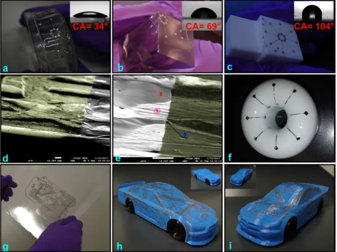
demonstrate the robustness of the water transfer printing method, aluminum ribbons have been transferred to 3D objects showing a broad range of surface energy. Standard glass (Pyrex), PMMA (poly(methyl methacrylate)) and Teflon have been chosen for their well-known surface energy values equal 68 mN/m,23 38 mN/m24 and 22 mN/m,25 respectively. Optical pictures in
figures 2a, 2b and 2c show that aluminum ribbons are successfully transferred whatever the material wetting behavior of the 3D object is (water contact angle values are equal to 34°, 69° and 104°, for glass, PMMA and Teflon, respectively). Interestingly, aluminum ribbons can be successfully transferred to the curved shapes (concave and convex) of a glass beaker, the edge of a PMMA cube or the face of a Teflon cube. Moreover, the transfer process is reproducible and robust for these materials.
Figure 2d and 2e, show Scanning electron microscope (SEM) images of aluminum ribbon transferred on a 50 cents euro coin. Figure 2d shows that the aluminum ribbon is firmly anchored along the edge of a star. The maximum thickness of the star equals 70µm (see 3D profile figure S6a) and wrapping capability is demonstrated. However, inevitably, micro-folds occur when film coats an arbitrary 3D complex surface. A zoom on aluminum ribbon edge (figure 2e) shows that different behaviors can be distinguished when highly different morphologies are involved. The area marked by the number 1 shows a low and relatively homogeneous roughness (RMS equals to 0.8µm; see 3D profile in figure S6b). In that case, aluminum ribbon wraps intimately the object morphology. The area marked by the number 2 shows a steep step on the surface and the aluminum ribbon is locally released from the object.
Interestingly, the area marked by the number 3 shows a sharp ridge that induced extreme bending radius as low as several microns (see in 2D profiles in figure S6c,d,e,f and g). Note that, such interesting bending capabilities are allowed because no rigid substrate is used during the transfer step. Indeed, according to the strain theory,26 the strain level induced in the
aluminum ribbon during the transfer is lower using water transfer printing than using conventional flexible substrate. Moreover, as shown in figure S7, interconnects have been transferred on human hair without mechanical and electrical failure.
Figure 2f shows the optical picture of aluminum ribbons that conformally wrapped the Teflon ring. The outside and inside diameters of Teflon ring equal 5cm and 1.4cm, respectively. The ring is a convenient shape to demonstration the advantages of water transfer printing technology. As shown in the figure S1 of the supplementary file, aluminum ribbons patterned on a flexible substrate cannot intimately wrap a holed surface such as a ring. Indeed, the conformal behavior suffers from the flexible substrate that covers the hole. Such drawback does not exists using the water transfer printing technique because the rigid substrate is dissolved during the transfer step. Note that, in this case, no polymeric mesh layer has been added to the star shaped pattern in order to avoid additional layer acting as flexible substrate. Figure 2g shows inkjet-printed silver (Ag) interconnects on A4 sized PVA substrate (21×29.7 cm). Water transfer printing has been successfully performed to wrap metallic wires around hand-sized plastic model car. Figures 2h and 2i show optical pictures of the model car before and after the transfer step proving large-scale processing capability.
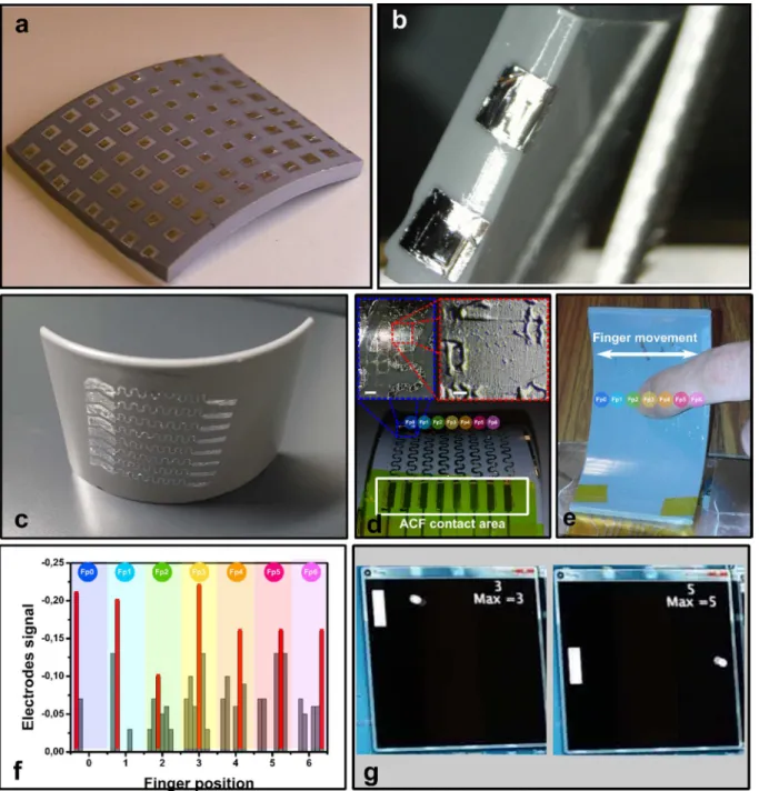
In order to demonstrate the water transfer printing technique potential applications, usual passive devices (MIM capacitors) have been successfully transferred to a bent shape (radius of curvature equals to 5 cm, Figure 3a) and to the edge (approximately 90°) of a plastic object (Figure 3b). These capacitors are composed of two 150nm-thick aluminum layers (top and bottom electrodes) and a 1.3 µm polymeric layer (dielectric) leading to a capacitance of about
34pF. Electrical characteristics after the transfer step are reported in Figure S8. Finally, a capacitive touchpad has been fabricated on a bent plastic object. The 3D object bending radius equals 5cm. Figure 3c shows the capacitive touchpad conformally wrapped around the object. The sensing area (4cm×1cm) is defined by eight aligned electrodes (5mm×1cm) in order to detect finger sliding. V-shaped electrodes design is used to optimize the overlap between 1mm spaced electrodes. In order to respect the inter-electrodes distance, a polymeric mesh layer has been printed for previously mentioned reasons. The blue inset of figure 3d shows the aforementioned electrodes and the red inset shows that aluminum electrodes intimately wrap the 3D plastic object and polymeric mesh. Note that, blistered shapes shown in the blue inset are due to the Su8 mesh under aluminum film. Indeed, Su8-based ink suffers from the well-known coffee ring effect. However, no mechanical failure was observed showing the robustness of the water transfer printing technology. Moreover, for external acquisition, an anisotropic conductive film (ACF 3M ECATT 9706) was used to connect the capacitive touchpad to a silver ribbon cable printed on Kapton. The capacitive touchpad has been transferred to the convex side of the curved object. As shown in figure 3e, the finger slides on the opposite side, faced to the electrodes, changing initial capacitance value. Arduino development board, connected to a computer via serial USB communication, has been used to measure the capacitance value between each electrode. Capacitances (Cn), are firstly measured using microcontroller analog
outputs/inputs. Time constants (τn) of capacitors discharge τn = RCn are then estimated, where
R is the pull-up internal resistor of the microcontroller.
As shown in figure 3f, when the finger position (Fpn) faces a capacitor (Cn), capacitance value
decreases. Cn is then the most impacted (red bars) by Fpn enabling finger position sensing. One
can note that neighboring capacitors are also, to a lesser extent, impacted by the finger (grey bars), depending on how it is placed. Moreover, a pong game using capacitive sensor as a
remote has been demonstrated using “Processing” software (see figure 3g and Video S3 in supplementary file).
In conclusion, we have demonstrated an industrially viable technology to intimately wrap thin films around 3D objects. Water transfer printing technology also named hydrodipping has been adapted from graphic arts to conformal electronics. The adapted process allows the fabrication of electronics on 2D substrate using conventional microelectronics materials and methods. Films can be transferred to many kinds of surfaces including plastic, metal, woods, all those which can be dipped into water. Thin films have been successfully patterned at lithographical accuracy or by inkjet printing over a large-area showing the versatility of the concept. Metallic and polymeric thin films have been successfully wrapped around random 3D shapes whose materials show a wide span of wetting properties. Moreover, water transfer printing enables highly bended thin films because no rigid substrate is required during transfer step. Importantly, this technology has clearly solved a challenging issue in the field of conformal electronics. Indeed, patterns have been wrapped around a 3D holed object. The bent touchpad and metal/insulator/metal capacitors, demonstrate potential applications of this technology. We demonstrated that daily-life hand-sized objects are compatible with the aforementioned technique. We assume that the presented technique is only limited by the materials depositions equipment scale in view of a larger area processing.
ACKNOWLEDGMENTS
This work is supported by the European Union through the European Regional Development Fund (ERDF), and by the French region of Brittany (project: IMPRIM’). We thank, R. Beal (ISTIC Fablab) and S. Pernon (Université de Rennes 1 - ISTIC) for part dealing with 3D printing.
Figure 1: Patterned thin films wrapping 3D object using water-transfer process.
Schematics showing: a) multilayered films patterned on water-soluble substrate (generic structure); b) water-soluble substrate deposited on top of the water-filled dip tank; c) 3D object is dipped through the patterns after PVA dissolution; d) a 3D object is gently shacked into the water, after a few seconds the object can be withdrawn from water; optical pictures showing: e) water-soluble substrate deposition on top of the water; f) PVA substrate floating on top of the water; g) PVA substrate at the beginning of the dissolution; h) patterns floating after PVA complete dissolution; i) object dipping; j) patterns wrapping 3D object.
Figure 2: Process capabilities. Optical observations of patterns conformally transferred to: a)
glass beaker; b) PMMA cube; c) Teflon cube; d) SEM observations of ribbons wrapped around 50 cents euro coin: Aluminum ribbons anchored along the edge of a 70µm thick star; e) edge of ribbons firmly anchored when surface morphology is submicronic; Mark 1 shows area with RMS value equals 0.8µm, Mark 2 shows area where aluminum is released due to 70µm thick step, mark 3 shows aluminum film along a 10µm sharp ridge; f) optical observation of ribbons wrapped around Teflon ring; g) Inkjet-printed silver interconnects on A4 size commercial PVA
substrate. 3D printed model car (16×4×4cm, plastic) before (insets) and after water transfer process; h) right-hand and; i) left-hand side views of the model.
Figure 3: Capacitive devices on curved objects. a) Optical picture of 3-layers MIM capacitors
transferred to a bent sheet of plastic; b) optical picture of MIM capacitors at the edge of a plastic object. Active layer conformally wraps object, forming a 90° angle; c) optical picture of aluminum-based capacitive sensors transferred to bent plastic object; d) top-view of the device
showing sensing area, interconnects and electrical contact area (anisotropic conductive film, (ACF) enabling external measurements. Each capacitor is highlighted by Fp marks. Blue inset shows a zoom on 1mm spaced electrodes (scale bar is equal to 1mm) and red inset highlights conformal wrapping of aluminum film around plastic (scale bar equals 200µm). Note that observed blistered lines are part of polymeric squared mesh; e) back-side of the bent object showing finger sliding along the sensors area (Fp0 to Fp6); f) normalized capacitance values (Cn) as a function of finger position (Fpn) enabling finger position detection. Red bars
correspond to capacitor variation due to finger presence; g) Screen shots showing sensors used as remote to play pong game.
ASSOCIATED CONTENT
Supporting Information:
Experimental section:
a) Description of optical and profilometry equipement b) PVA processing
c) Thin film patterning
Figure S1. Optical pictures showing aluminum ribbons patterned on PEN substrate (25µm
thick) that are transferred to Teflon ring
Figure S2. Electrodes patterned using conventional photoresists and water-free chemical
reagents.
Figure S3. Optical pictures showing silver ink printed on PVA substrate for large-area
Figure S4: PVA dissolution behavior as function of process variants.
Figure S5. Electrodes transferred to curved glass.
Figure S6: Aluminum conformal wrapping around 50 cents euro coin.
Figure S7: Aluminum interconnects wrapped around human hair
Figure S8: MIM capacitors wrapped over 3D object.
Video S1: 76s-movie at 25 frame/s showing Water Transfer Printing concept.
Video S2: 205s-movie at 25 frame/s showing 3-axis machine assisted water transfer printing
technology.
Video S3: 12s-movie at 25 frame/s showing bent touchpad as remote to play pong game.
AUTHOR INFORMATION
Corresponding Author
* E-mail: [email protected]
Notes
The authors declare no competing financial interest.
Author Contributions
The manuscript was written through contributions of all authors. All authors have given approval to the final version of the manuscript.
REFERENCES
(1) Yeo, W.-H.; Kim, Y.-S.; Lee, J.; Ameen, A.; Shi, L.; Li, M.; Wang, S.; Ma, R.; Jin, S.H.; Kang Z.; Huang Y.; Rogers J.A.; Multifunctional Epidermal Electronics Printed Directly Onto the Skin. Adv. Mater., 2013, 25, 2773–2778.
(2) Jeong, S. H.; Zhang, S.; Hjort, K.; Hilborn, J.; Wu, Z.; PDMS-Based Elastomer Tuned Soft, Stretchable, and Sticky for Epidermal Electronics. Adv. Mater., 2016, 28, 5830–5836.
(3) Xu, B.; Akhtar, A.; Liu, Y.; Chen, H.; Yeo, W.-H.; Park, S.I.; Boyce, B.; Kim, H.; Yu, J.; Lai, H.-Y.; Jung, S.; Zhou, Y.; Kim, J.; Cho, S.; Huang, Y.; Bretl, T.; Rogers, J.A.; Flexible Electronics: An Epidermal Stimulation and Sensing Platform for Sensorimotor Prosthetic Control, Management of Lower Back Exertion, and Electrical Muscle Activation. Adv. Mater., 2016, 28, 4462–4471.
(4) Kim, D.-H.; Viventi, J.; Amsden, J.J.; Xiao, J.; Vigeland, L.; Kim, Y.-S.; Blanco, J.A.; Panilaitis, B.; Frechette, E.S.; Contreras, D.; Kaplan, D.L.; Omenetto, F.G.; Huang, Y.; Hwang, K.C.; Zakin, M.R.; Litt, B.; Rogers, J.A.; Dissolvable Films of Silk Fibroin for Ultrathin Conformal Bio-Integrated Electronics. Nat. Mater., 2010, 9, 511–517.
(5) Kim, J.; Lee, M.; Shim, H. J.; Ghaffari, R.; Cho, H.R.; Son, D.; Jung, Y.H.; Soh, M.; Choi, C.; Jung, S.; Chu,K.; Jeon, D.; Lee, S.-T.; Kim, J.H.; Choi, S.H.; Hyeon, T.; Kim, D.-H.; Stretchable Silicon Nanoribbon Electronics for Skin Prosthesis. Nat. Commun., 2014, 5, 5747– 5758.
(6) Song, Y. M.; Xie, Y.; Malyarchuk, V.; Xiao, J.; Jung, I.; Choi, K.-J.; Liu, Z.; Park, H.; Lu, C.; Kim, R.-H.; Li, R.; Crozier, K.B.; Huang, Y.; Rogers, J.A.; Digital Cameras with Designs Inspired by the Arthropod Eye. Nature, 2013, 497, 95–99.
(7) Li, Z.; Wang, Y.; Xiao, J.; Mechanics of Curvilinear Electronics and Optoelectronics. Curr. Opin. Solid State Mater. Sci., 2015, 19, 171–189.
(8) Sekitani, T.; Nakajima, H.; Maeda, H.; Fukushima, T.; Aida, T.; Hata, K.; Someya, T.; Stretchable Active-Matrix Organic Light-Emitting Diode Display Using Printable Elastic Conductors. Nat. Mater., 2009, 8, 494–499.
(9) Vosgueritchian, M.; Tok, J.B.-H.; Bao, Z.; Stretchable LEDs: Light-Emitting Electronic Skin. Nat. Photonics, 2013, 7, 769–771.
(10) Kaltenbrunner, M.; White, M.S.; Glowacki, E.D.; Sekitani, T.; Someya, T.; Sariciftci, N.S.; Bauer, S.; Ultrathin and Lightweight Organic Solar Cells with High Flexibility. Nat. Commun., 2012, 3, 770-777.
(11) Rogel, R.; Le Borgne, B.; Mohammed-Brahim, T.; Jacques, E.; Harnois, M.; Spontaneous Buckling of Multiaxially Flexible and Stretchable Interconnects Using PDMS/Fibrous Composite Substrates. Adv. Mater. Interfaces, 2017, 4, 1600946.
(12) Stoppa, M.; Chiolerio, A.; Wearable Electronics and Smart Textiles: A Critical Review. Sensors, 2014, 14, 11957–11992.
(13) Park, Y.J.; Lee, S.-K.; Kim, M.-S.; Kim, H.; Ahn, J.-H.; Graphene-Based Conformal Devices. ACS Nano, 2014, 8, 7655–7662.
(14) Salvatore, G.A.; Münzenrieder, N.; Kinkeldei, T.; Petti, L.; Zysset, C.; Strebel, I.; Büthe, L.; Tröster, G.; Wafer-Scale Design of Lightweight and Transparent Electronics that Wraps Around Hairs. Nat. Commun., 2014, 5, 2882-2890.
(15) Feiner, R., Engel, L.; Fleischer, S.; Malki, M.; Gal, I.; Shapira, A.; Shacham-Diamand, Y.; Dvir,T.; Engineered Hybrid Cardiac Patches with Multifunctional Electronics for Online Monitoring and Regulation of Tissue Function. Nat. Mater., 2016, 15, 679–685.
(16) Fukuda, K.; Takeda, Y.; Yoshimura, Y.; Shiwaku, R.; Tran, L.T.; Sekine, T.; Mizukami, M.; Kumaki, D.; Tokito,S.; Fully-Printed High-Performance Organic Thin-Film Transistors and Circuitry on One-Micron-Thick Polymer Films. Nat. Commun., 2014, 5, 4147-4155.
(17) Ko, H.C.; Shin, G.; Wang, S.; Stoykovich, M.P.; Lee, J.W.; Kim, D.-H.; Ha, J.S.; Huang, Y.; Hwang, K.-C.; Rogers, J.A.; Curvilinear Electronics Formed Using Silicon Membrane Circuits and Elastomeric Transfer Elements. Small, 2009, 5, 2703–2709.
(18) Zhang,Y.; Xu,S; Fu, H.; Lee,J.; Su,J.; Hwang, K.-C.; Rogers, J.A.; Huang, Y.; Buckling in Serpentine Microstructures and Applications in Elastomer-Supported Ultra-Stretchable Electronics with High Areal Coverage. Soft Matter, 2013, 9, 8062–8070.
(19) Lee, S. K.; Kim, B. J.; Jang, H.; Yoon, S. C.; Lee, C.; Hong, B. H.; Rogers, J.A.; Jeong, H.C.; Ahn, J. H.; Stretchable Graphene Transistors with Printed Dielectrics and Gate Electrodes. Nano Lett., 2011, 11, 4642-4646.
(20) Zhang, Y.; Gui, Y.; Meng, F.; Li, L.; Gao, C.; Zhu, H.; Hao, Y; Graphene Water Transfer Printing for 3D Surface. Micro Electro Mechanical Systems (MEMS), 2016 IEEE 29th International Conference, Shanghai, 13-16.
(21) Robin, M.; Kuai, W.; Amela-Cortes, M.; Cordier, S.; Molard, Y.; Mohammed-Brahim, T.; Jacques, E.; Harnois, M.; Epoxy Based Ink as Versatile Material for Inkjet-Printed Devices. ACS Appl. Mater. Interfaces, 2015, 7, 21975-21984.
(22) Hur, S.-H.; Khang, D.-Y.; Kocabas, C.; Rogers, J.A.; Nanotransfer Printing by Use of Noncovalent Surface Forces: Applications to Thin-Film Transistors that Use Single-Walled Carbon Nanotube Networks and Semiconducting Polymers. Appl. Phys. Lett., 2004, 85, 5730-5732.
(23) Chou, J.; Mcallister, M.; Schottland P.; (Sun Chemical), EP 2649141 A2, 2013.
(24) Kwok, D.Y.; Leung, A.; Lam, C.N.C.; Li, A.; Wu, R.; Neumann, A. W.; Low-Rate Dynamic Contact Angles on Poly(methyl methacrylate) and the Determination of Solid Surface Tensions. J. Colloid Interface Sci.,1998, 206, 44–51.
(25) Fu, R.K.Y.; Mei, Y.F.; Wan, G.J.; Siu, G.G.; Chu, P.K.; Huang, Y.X.; Tian, X.B.; Yang, S.Q.; Chen, J.Y.; Surface Composition and Surface Energy of Teflon Treated by Metal Plasma Immersion Ion Implantation. Surf. Sci., 2004, 573, 426–432.
(26) Gleskova, H.; Wagner, S.; Suo, Z.; Failure Resistance of Amorphous Silicon Transistors under Extreme In-Plane Strain. Appl. Phys. Lett., 1999, 75, 3011 – 3013.