HAL Id: hal-02793716
https://hal.archives-ouvertes.fr/hal-02793716
Submitted on 2 Dec 2020HAL is a multi-disciplinary open access archive for the deposit and dissemination of sci-entific research documents, whether they are pub-lished or not. The documents may come from teaching and research institutions in France or abroad, or from public or private research centers.
L’archive ouverte pluridisciplinaire HAL, est destinée au dépôt et à la diffusion de documents scientifiques de niveau recherche, publiés ou non, émanant des établissements d’enseignement et de recherche français ou étrangers, des laboratoires publics ou privés.
Competition between V2O3 phases deposited by
one-step reactive sputtering process on polycrystalline
conducting electrode
J.A.J. Rupp, E. Janod, M.-P. Besland, B. Corraze, A. Kindsmüller, M.
Querre, J. Tranchant, L. Cario, R. Dittmann, R. Waser, et al.
To cite this version:
J.A.J. Rupp, E. Janod, M.-P. Besland, B. Corraze, A. Kindsmüller, et al.. Competition between V2O3 phases deposited by one-step reactive sputtering process on polycrystalline conducting electrode. Thin Solid Films, Elsevier, 2020, 705, pp.138063. �10.1016/j.tsf.2020.138063�. �hal-02793716�
Title 1 Competition between V2O3 Phases Deposited by One‐Step Reactive Sputtering Process on 2 Polycrystalline Conducting Electrode 3 4 Authors 5 J. A. J. Rupp, E. Janod, M.‐P. Besland, B. Corraze, A. Kindsmüller, M. Querré, J. Tranchant, 6 L. Cario, R. Dittmann, R. Waser, D. J. Wouters 7 8 Affiliations 9 J. A. J. Rupp, Dr. D. J. Wouters, A. Kindsmüller, Prof. Dr. R. Waser: RWTH Aachen University & 10 JARA‐FIT Germany 11 Prof. Dr. R. Dittmann, Prof. Dr. R. Waser: PGI‐7 Research Center Jülich & JARA‐FIT Germany 12 Dr. M. Querré, Dr. M.‐P. Besland, Dr. E. Janod, Dr. L. Cario, Dr. J. Tranchant : Institut des 13 Matériaux Jean Rouxel (IMN) Université de Nantes, CNRS, France 14 15 Abstract 16 This comprehensive work investigates a technologically appealing synthesis of V2O3 oxide thin 17 films for electronic applications by the use of direct reactive sputtering with a heavily diluted 18
gas mixture on a conducting platinum electrode. Morphological characterization was
19
performed by Scanning Electron Microscopy, Atomic Force Microscopy , X‐Ray Diffraction and
20
X‐Ray Reflectometry. Vanadium valence states were investigated by X‐Ray Photoelectron
21
Spectroscopy and crystalline phases were checked by X‐Ray Grazing Incidence measurements.
22
Low temperature electrical transport characteristics were determined by 2‐point probe
23
measurements. Only amorphous V2O3 was found to exist in a mixed‐valence phase in the
investigated parameter range. Deposition temperatures between 400 °C and 550 °C enable
1
formation of mixtures between crystallographic phases of corundum‐ and bixbyite‐type V2O3
2
polymorphs. Depending on temperature and sputtering power, morphology and
3
stoichiometry can be tuned to generate four distinct type of electrical transport
4 characteristics. Most promising electrical properties of corundum V2O3 with a resistance ratio 5 of up to four orders of magnitude (during the low temperature insulator‐to‐metal transition) 6 have been obtained for a moderate sputtering power of 50 W (on a 1” target) at a deposition 7
temperature of 600 °C. Reactive sputtering thus enables direct control of structural and
8 electrical parameters for polycrystalline V2O3 thin film phases on a conducting substrate. 9 10 Key Words 11 Vanadium Oxide, Vanadium Sesquioxide, V2O3, Reactive Sputtering, Bixbyite. 12 13 1. Introduction 14 The vanadium‐oxygen system comprises a large variety of over 20 thermodynamically stable 15 crystalline phases throughout the range of oxygen content [1]. Most of these phases exhibit 16 fascinating chemical and physical features that open a large field of technical applications [2]. 17 For instance, vanadium based oxides have attracted much attention in energy storage systems 18
operating with lithium and sodium batteries [3] which are regarded as the most promising
19
electrochemical storage technologies. Furthermore, the famous low oxygen content phase of
20
VO2 was widely proposed for usage in optical [4][5] and electrical switches [6][7]. Yet,
21
controlled synthesis of phases with uniform stoichiometry (in particular phases with a low
22
oxygen to vanadium ratio of O:V < 2.5) is highly challenging because it requires precise control
23
of low oxygen partial pressures p(O2) besides the need for high crystallization temperatures. 24
corundum V2O3 which undergoes an insulator‐to‐metal transition (IMT) at 155 K from a 1 paramagnetic metallic phase to a low temperature antiferromagnetic insulating monoclinic 2 phase [8]. The crystallographic phase change leads to a drop of the c/a ratio and a volume 3 increase of about 1.2 % accompanied by a change in resistivity up to six orders of magnitude. 4 More interestingly, under tensile strain, V2O3 is regarded being an archetype Mott‐Hubbard 5 insulator [8]. On atomic scale, an equivalent negative (chemical) pressure can be ensured by 6 doping of V2O3 with over 1.1 at. % chromium. This kind of material can realize an IMT without 7 crystallographic phase change which can be driven not only by pressure or temperature [8] 8
but also by an electric potential [9]. While transitions of pure vanadium oxide phases are
9
volatile phenomena [10][11], non‐volatile resistive switching could be realized as well in Cr‐
10
doped V2O3 with at least 5 at. % Cr [12]. This makes the family of vanadium oxides (and
11
especially un‐doped and Cr‐doped V2O3) an interesting candidate for the fabrication of
12
electrical devices for neuromorphic [13] and memory applications [12].
13
In the past, many different synthesis methods have been involved to obtain low oxygen
14
content phases such as V2O3. Typically, equilibrium synthesis relies on a two‐step approach
15
with deposition and subsequent reduction, e.g. thermal reduction [14], oxygen buffer
16
reduction [15] or plasma hydrogen reduction [16]. Alternatively, direct deposition of low
17 oxygen content phases is only achieved by non‐equilibrium synthesis, e.g. molecular beam 18 epitaxy [17][18], electron beam evaporation [19][20][21] or reactive sputtering [22][23]. For 19 various techniques, it has been confirmed that the oxygen partial pressure mainly determines 20
the phase to be formed [24][25][26][27]. Previous works with direct deposition methods
21
typically used substrate temperatures between 700 °C [28][29] and 1700 °C [24] to ensure
22
satisfying thin film crystalline quality. With reactive sputtering, we chose a deposition
23
technique compatible with a standard CMOS fabrication and giving access to a large range of
physical layer properties such as morphology, roughness and density. Strong deviations from 1 well‐known bulk properties have already been identified for “ideal” epitaxial V2O3 thin films 2 grown on insulating sapphire due to various effects such as porosity [30] and residual stress 3 [24]. For technological purposes in electronic devices, the physical properties of V2O3 thin films 4
should further be investigated in polycrystalline form on a polycrystalline conducting
5
electrode. Using a conducting electrode as substrate can ensure an electrical contact for the
6
fabrication of resistively switching devices based on a capacitor structures in a desired vertical
7
metal‐insulator‐metal (MIM) geometry. Apart from the deposition of aforementioned
8 crystalline films, amorphous oxide semiconductors are a hot topic in materials science and 9 engineering as well [31] thanks to their highly promising benefits such as lowest deposition 10 temperature, high resistivity, low roughness and attainable uniform and isotropic properties. 11 Therefore, the realization of amorphous Cr‐doped V2O3 thin films as “precursor” is a further 12 valuable goal that is of interest e.g. for selector devices [32][33]. 13 Here we present a comprehensive and systematic optimization of a direct deposition method 14
for V2O3 in amorphous and crystalline form on a conducting electrode. For the lowest
15
deposition temperature at room temperature, V 3+ valence only manifests in combination
16
with +2 or +4 valences for the investigated parameters. Crystalline V2O3 could be achieved at
17
a minimum deposition temperature of 400 °C. However, slight variations in oxygen partial
18
pressure lead to additional formation of metastable bixbyite‐type V2O3 up to 550 °C. A
19 moderate sputtering power of 50 W and a deposition temperature of 600 °C resulted in pure 20 corundum V2O3 phase with a clear insulator‐to‐metal transition and resistance ratio of four 21 orders of magnitude. Direct reactive sputtering can thus be considered as a valuable technique 22 to control structural and electrical features of V2O3 thin films on a conducting substrate such 23
as platinum. Moreover, it gives a physical synthesis method for the metastable compound of 1 bixbyite V2O3. 2 3 2. Experimental 4 Various vanadium oxide thin films (with a thickness ranging from 30 nm to 120 nm) have been 5 deposited on a 30 nm thick platinum bottom layer by radio frequency (RF) reactive magnetron 6 sputtering of a one inch vanadium target. Off‐axis co‐sputtering with an incident angle of 15° 7
was used. The target to substrate distance was fixed at 5 cm. The base pressure was held
8
below pbase < 1 nbar and the working pressure was fixed at pprocess = 10 µbar. The oxygen
9 partial pressure p(O2) was adjusted with a flux ratio of two mass flow controllers: pure Argon 10 and an Oxygen/Argon mixture allowing various flow rate ratios: 100/0 (with access to a p(O2) 11 ranging from 1000 to 100 nbar), 10/90 (100 nbar to 10 nbar range) or 1/99 (10 nbar to 1 nbar 12 range). With such ratios, the used oxygen partial pressure was straightforwardly calculated 13
with the assumption of an ideal gas. This method allowed control of the p(O2) down to a
14
few nanobar. Several series of vanadium oxide thin films were deposited as summarized in
15
Table 1 to 4: three sample series were fabricated while varying oxygen partial pressure
16 between 1000 nbar and 1 nbar. The sample “series 1” was sputtered at room temperature 17 (T = 30 °C, P = 100 W, Table 1) and two samples “series 2” and “series 3” were sputtered at 18 elevated substrate temperatures with different sputtering powers P (T = 400 °C, P = 100 W, 19 Table 2 and T = 400 °C, P = 50 W, Table 3, respectively). Two sputtering power values were 20
investigated since a strong increase in deposition rate by one order of magnitude was
21
obtained in the lower oxygen partial pressure range (see Figure 1). A fourth sample “series 4”
22
explores the temperature dependence of V2O3 from room temperature up to 600 °C for a
23
p(O2) of 10 nbar (Table 4) with a deposition power of 50 W. For the fifth series 5 (not shown)
deposited with a power of 100 W (i.e. increase of sputtering power by a factor of two),
1
crystalline phases were determined by XRD. For the determination of the thickness of
2
vanadium oxide films (and calculation of their deposition rate), X‐ray reflectometry (XRD:XRR)
3
was performed with an X‐ray diffractometer by PANalytical. The thickness was extracted by
4
evaluation of the Kiessing fringes of the relevant vanadium oxide layer on the substrate.
5
Densities of vanadium oxide thin films were simulated with the obtained intensity reflection
6
profile and the software X’pert reflectivity from PANalytical. Hereby, a substrate stack of SiO2
7
(thickness d = 600 µm, density ρ = 2.32 g/cm³, mean root square roughness Rms = 0 nm)
8
followed by an adhesion layer TiOx (d = 5±1 nm, ρ = 3.28 g/cm³, Rms = 0‐1 nm) and the
9
electrode Pt (d = 30 nm, ρ = 21.2 g/cm³, Rms = 0‐1 nm) served as input with given simulation
10
constraints. During the segmented fit, values for thickness, density and roughness of the
11
vanadium oxide film on top of the substrate were kept variable. For selected samples, the
12
vanadium valence was determined as function of oxygen partial pressure by X‐ray
13
photoelectron spectroscopy (XPS) at a “PHI 5000 Versa Probe II” from Ulvac‐Phi, Inc. with an
14
energy resolution better than 0.2 eV. Peaks were normalized to the C 1s binding energy of
15
residual carbon. In particular, vanadium V2p core level spectra were recorded and
16
stoichiometry was determined while comparing obtained spectra with integer vanadium
17
oxidation states. These binding energies were determined by analysing reference samples of
18
crystalline vanadium oxide thin films V2O5, VO2, V2O3 and VO, (see Table 2&3) as well as
19 through comparison with literature values[34][35]. To avoid photoelectron signal from native 20 oxidation after sputtering, vanadium oxide thin films were capped in situ by a 100 nm thick Au 21 layer. The capping layer was further stripped off with scotch tape and manipulator in the XPS 22 chamber high vacuum system right before the measurement. The pure vanadium thin film 23
(without capping layer) was etched by Argon ion sputtering to remove native oxidation.
Oxidation states of amorphous VOx thin films were determined for some critical p(O2) values 1 (where major changes in deposition rate were observed) by XPS. Due to the complex shape of 2 V 2p core level spectra of vanadium oxide phases, fitting was not performed. Oxidation states 3 are here discussed qualitatively by their energy position with respect to integer valence states. 4 For crystalline thin films, crystallographic phases were determined using X‐ray diffractometry 5 in grazing incidence geometry XRD:GI with a diffractometer “X’Pert PRO” from PANalytical 6
with a Cu‐Kα source. The volume ratio of corundum and bixbyite V2O3 was determined by
7 refinement of diffraction patterns via PowderCell software. The use of grazing incidence mode 8 and a possible preferential orientation of corundum V2O3 results in an uncertainty of about 9 ± 5 vol. %. Thus, given estimations should be considered as qualitative guideline. To determine 10
the optical reflectance of the deposited films, Light Microscopy images were taken in a
11
controlled environment (clean room yellow lightning, constant brightness and contrast) at
12
magnification 50 by an “Olympus MX 50” microscope. Morphology was determined by
13
scanning electron microscopy (SEM) using a Zeiss “DSM982 GEMINI” electron microscope with
14
an operating voltage of 10 kV. Grain sizes were determined using the line section method with
15
SEM images and roughness was quantified using an atomic force microscope (AFM) from
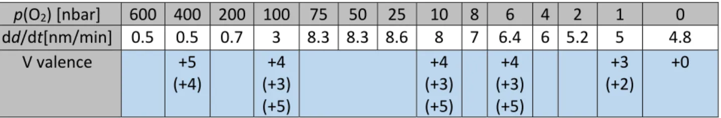
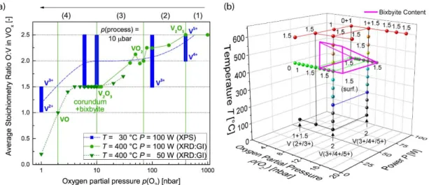
16 Veeco “di CP II”. Low temperature electrical transport characteristics were performed with a 17 modified closed‐cycle Helium circuit cryostat “Omniplex DE210” from ARS. 18 19 3. Results 20 In Table 1, deposition rates dd/dt as well as detected vanadium valences are given for samples 21 sputtered at room temperature (30 °C) as a function of oxygen partial pressure. Numbers in 22
brackets give secondary valence states with minor quantitative occurrence. Table 2 and 3
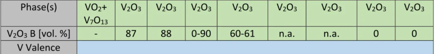
23
summarize deposition rates, detected phases as well as analysis of vanadium valences of
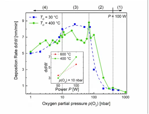
samples sputtered at 400 °C for samples sputtered at 100 W and 50 W, respectively. In the 1 following sections, the trends of physical parameters of deposited films will be presented and 2 discussed. 3 4 3.1 Deposition Rates of Thin Films Sputtered at 30 °C / 400 °C / 600 °C 5 In Figure 1, the deposition rate is plotted as function of logarithmic oxygen partial pressure 6
for samples sputtered at room temperature (blue squares) and at 400 °C (green dots)
7 (series 1&2). For samples sputtered at room temperature (blue squares), four distinct regimes 8 can be identified (labelled as zones (1) to (4)): In the case of a high oxygen partial pressure of 9 400 nbar, a very slow deposition rate of 0.5 nm/min is obtained which slightly decreases with 10 increasing p(O2) (zone (1)). Towards lower oxygen partial pressure (zone (2)), the deposition 11 rate increases by one order of magnitude up to 8.8 nm/min and reaches its maximum at a 12
p(O2) of 100 nbar. In an intermediate regime in zone (3) (for a p(O2) between 100 nbar and
13
10 nbar), the deposition rate stays constant whereas for oxygen partial pressures below
14 10 nbar (zone (4)), the deposition rate drops to a value of 5 nm/min. For thin films deposited 15 at 400 °C (green dots), one can observe a similar trend as for the ones sputtered at 30 °C for 16 the same sputtering power of 100 W. In contrast to thin films sputtered at room temperature, 17 a stronger variation of absolute deposition rate values spans up a range of ~2 nm/min. For 18 thin films sputtered with half the power on the target (50 W, Figure 1 inset), the deposition 19 rate is decreased by a factor of two (3.3 nm/min) as compared to the rate obtained at 100 W 20 (6.7 nm/min). Furthermore, a variation of deposition temperature from 400 °C to 600 °C only 21 leads to a marginal change in deposition rate at low power of 50 W (~0.5 nm/min) but a more 22 significant one at a higher power of 100 W (~1.5 nm/min). 23 24
3.2 Phase Analysis of Thin Films Sputtered at 30 °C / 400 °C / 600 °C
1
Figure 2 (a)‐(d) display XRD:GI patterns of thin films sputtered at 400 °C with integer vanadium
2
valence across the entire investigated oxygen partial pressure range. In most cases of
3
investigated thin films, a mixture of at least two different phases was obtained (as summarized
4
in Table 2&3). For certain conditions of oxygen partial pressure (Figure 2), pure vanadium
5
oxide phases were detected with V2O5 (400 nbar, (a)), VO2 (70 nbar, (b)), V2O3 (6 nbar, (c)) and
6
V2O2 (2 nbar, (d)). Concerning XPS analysis, records of the V 2p core level are plotted in
7
Figure 2(e)‐(h) for thin films deposited at different substrate temperatures and oxygen partial
8
pressures. For the highest p(O2) (400 nbar) and a deposition temperature of 400 °C (Figure 2e
9
green curve), vanadium V 2p core level spectra reveal a peak with a symmetric shape
10
associated to a single valence of V 5+ for V 2p1/2 as well as V 2p3/2. For the same pressure
11
value and room temperature deposition (Figure 2e blue curve), a slight shift is recorded and
12
significant for a major valence of V 5+ with a minor component of V 4+ at lower binding
13
energy. Thin films sputtered at room temperature for three values of p(O2) (100 nbar, 10 nbar
14
and 6 nbar, Figure 2f) display very similar spectra with broad maxima located at a binding
15
energy associated to V 4+, meaning that components associated to V 5+ and V 3+ might also
16
have a contribution. In addition, the spectrum of a V2O3 thin film of sputtered at 600 °C and a
17
p(O2) of 10 nbar is given (red curve in Figure 2f). One can observe a shift of the broad
18
maximum of V 2p1/2 to a slightly lower binding energy associated with a shoulder located at
19
a binding energy of V 2+ (which is not recorded for thin films deposited at room temperature,
20
see blue curves). In the case of the thin film sputtered at 2 nbar p(O2) either at room
21
temperature or 400 °C (Figure 2g), one can observe a greater shoulder (~513 eV) of the
22
V 2p1/2 peak compared to crystalline V2O3 (Figure 2f red curve). Lastly, Figure 1h shows the
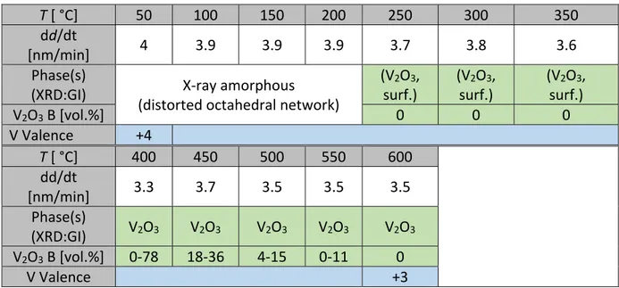
V 2p core level spectrum of a thin film sputtered at 0 nbar p(O2) (with an asymmetric peak 1 shape) as a reference for the V 2p binding energy of metallic vanadium. 2 3 3.3 Temperature Profile of Vanadium Oxides Sputtered at 10 nbar p(O2) 4
The last presented sample series 4 has been deposited with an oxygen partial pressure of
5 10 nbar and a sputter power of 50 W for increasing substrate temperature between 50 °C and 6 600 °C. Deposition rates, detected phases as well as analysis of vanadium valence are given in 7 Table 4. Phase analysis was performed for an additional series 5 (with a sputtering power of 8
100 W, not shown) where XRD‐analysis only exhibited diffraction peaks of corundum V2O3
9
(except for a deposition temperature of 400 °C where a mixture of bixbyite V2O3 was
10
obtained). In Figure 3a, the XRD patterns at grazing incidence angle are plotted versus
11
deposition temperature between 30 °C and 600 °C (with increasing value starting from the
12
bottom). As displayed in the bottom part of Figure 3a, the recorded pattern for samples
13 obtained in the 30 °C to 250 °C range only revealed diffraction peaks related to lattice planes 14 of cubic platinum [40] (resembling the bottom electrode) and can thus be characterized as X‐ 15 ray amorphous. As published previously [33], XPS‐analysis of a thin film deposited at room 16
temperature revealed a mixture of several vanadium valences ranging from +3 and +5
17
(compare Figure 2f). For a deposition temperature of 300 °C, diffraction peaks associated to
18
the crystallization of corundum V2O3 can be identified at Θ = 24,5 °, 33,2 ° and 54,3 ° which
19
correspond to {012}/{104}/{116} ‐ lattice planes. According to the JPCDS file of corundum
20
V2O3, these diffraction peaks possess the highest relative intensities (66 %, 100 %, 86 %) of the
21
corundum‐type V2O3 diffraction pattern [38]. Between 400 °C and 550 °C, several additional
22
diffraction peaks are recorded that predominantly belong to corundum‐type V2O3 (Figure 3a
23
black squares). Yet, some remaining diffraction peaks not belonging to corundum‐type V2O3
occur as well (Figure 3a marked by arrows). The diffraction peaks have been identified to 1 belong to a bixbyite‐type V2O3 [41] phase and were reproducibly observed in multiple samples. 2 Figure 3b compares the crystal structures of bixbyite‐ and corundum‐type V2O3 are illustrated 3 where grey spheres represent vanadium atoms and red spheres oxygen atoms. In addition, 4 Figure 3c shows a distinct X‐ray diffraction pattern of a thin film (sputtered at 450 °C) with the 5
two coexisting V2O3 phases (where red and black vertical lines identify diffraction peaks
6
associated to bixbyite and corundum V2O3 phases, respectively). Based on XRD‐analysis,
7
volume fractions of the two polymorphs were extracted by fitting diffraction profiles with
8 PowderCell (Figure 3d). As plotted, is appears that the higher content of bixbyite V2O3 phase 9 potentially reaches a maximum for a deposition temperature of 400 °C in our experimental 10 conditions and subsequently decreases for higher deposition temperatures. Interestingly, the 11
margin of volume fraction is the largest at this temperature and decreases with higher
12 deposition temperatures. For a deposition temperature of 600 °C, no bixbyite V2O3 phase has 13 been detected anymore. In contrast, for samples obtained at a sputtering power of 100 W in 14 the same oxygen partial pressure range (series 5), no bixbyite phase could be detected for the 15
same oxygen partial pressure except for a deposition temperature of 400 °C (see later in
16
Figure 6b). In the studied experimental range, the ratio between corundum and bixbyite phase
17
could vary considerably depending on deposition temperature, sputtering power and sample
18
batch. Major morphological changes were determined with respect to deposition
19
temperature by SEM imaging and are gathered in Figure 4a‐e. Deposition at room
20
temperature (Figure 4c) resulted in an amorphous columnar structure (i.e. the classical
21
expected morphology of sputtered thin films) with a relatively broad distribution of the lateral
22
grain size of 40 ± 20 nm. For a substrate temperature of 400 °C (Figure 4b), the thin film
23
possesses a similar columnar grain growth mode even when crystallized in pure corundum
V2O3 (verified by XRD:GI). At a higher substrate temperature of 600 °C (Figure 4a), a change in
1
growth mode to globular grains with larger grain size (58 ± 20 nm) is observable and the
2
crystalline quality as well as the corundum V2O3 phase content reach a maximum in the
3
investigated range. At an intermediate substrate temperature of 300 °C (Figure 4d) where XRD
4
analysis reveal emerging diffraction peaks in a mainly amorphous structure, grains with a
5
length of ~100 nm and a sharp surface structure start to grow on the surface of the amorphous
6
bulk thin film. Figure 4e illustrates the nanostructure of the surface of the thin film with most
7
prominent bixbyite content of 78 ± 5 vol. % (compare with the thin film of pure corundum
8
phase in Figure 4b). As shown, a mainly inhomogeneous morphology is formed with large
9
grains (~ 50 nm diameter) which consist of several smaller grains (~10 nm diameter). A
10
schematic evolution of phase coexistence in deposited vanadium oxide thin films is presented
11
in Figure 4f through light microscopy images (with respect to temperature at the bottom of
12
the graph) showing two distinct regions. Up to a deposition temperature of 400 °C, a
13
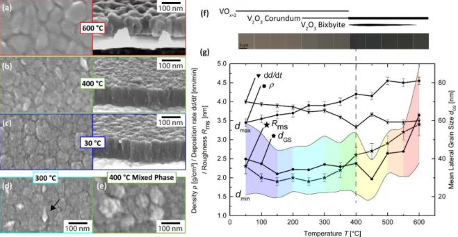
continuous change in contrast is observed that correlates with the increase in density
14
(Figure 4g squares). Using deposition temperatures above 400 °C (at the beginning of bulk
15 crystallization), samples display the common black color of bulk V2O3 [42]. The evolution of 16 thin film parameters (density ρ, deposition rate dd/dt, root mean square roughness Rms and 17 mean lateral grain size dGS) is plotted in Figure 4g as function of deposition temperature. The 18
colored area is a visual guideline for the distribution of grain sizes dGS. As fitted by XRR
19 measurements, the density ρ (Figure 4g dots) increases continuously from 3.5 to 4.5 g/cm³ 20 with increasing deposition temperature. A stable maximum (4.5 g/cm³) is reached at 500 °C. 21 Amongst amorphous films, roughness (star symbols) decreases continuously up to 150 °C. For 22 amorphous films, the highest root mean square roughness Rms (evaluated by AFM imaging) 23
was found for films deposited at room temperature (Rms = 2.4 nm) whereas for (partially)
crystalline films from 200 °C upwards, roughness increases continuously from Rms = 1.9 nm to
1
3.5 nm (in analogy to observed recrystallization at 600 °C, Figure 4a). At a deposition
2
temperature of 450 °C, a huge drop of average grain size dGS (pentagon symbols) and an
3 increase in deposition rate are observed; meanwhile, a large fraction of bixbyite V2O3 equal to 4 36 vol. % occurs. In the temperature range of bulk crystallization (400 °C up to 550 °C), grain 5 size barely increases up to 45 nm. Finally at 600 °C, as the pure corundum V2O3 is obtained, 6 the largest observed mean grain size > 60 nm is reached. 7 3.4 Morphology and Low Temperature Electrical Measurements of V2O3 8
In Figure 5, SEM images in top view and cross section (a) and low temperature electrical
9 transport properties (b) are reported for thin films deposited at 100 W and a p(O2) of 10 nbar 10 for three deposition temperatures (30 °C / 400 °C / 600 °C) and for a sputtering power of 50 W 11 for the case of 600 °C. 12 For the lowest deposition temperature without heating (30 °C and P = 100 W), amorphous VOx 13
exhibits a fine‐grained microstructure with a random grain orientation as shown in cross‐
14
section (Figure 5a(1)). The morphology is slightly different from the one observed for half the
15
sputter power of 50 W (Figure 4c) where columnar growth was highlighted. By increasing
16
deposition temperature to 400 °C (P = 100 W), numerous crystallite edges emerge on the
17
surface of a thin film (Figure 5a(2)) in agreement with crystallized V2O3 verified by XRD‐
18
analysis (not shown). In contrast to the thin film deposited at the lower power of 50 W
19
(Figure 4a), the density of crystallite edges on the surface increases considerably. At a
20
deposition temperature of 600 °C, grain size increases to a maximum for both used powers of
21
100 W (Figure 5a(3)) and 50 W (Figure 5a(4)). In this case, no significant change of morphology
22
is visible between the two deposition power values. To get further insights, the electrical
23
transport characteristics of the same films have been acquired (Figure 5b). A purely insulating
behaviour has been evidenced for the vanadium oxide thin film sputtered at room
1
temperature at low oxygen partial pressure (Figure 5b(1)). For V2O3 thin films sputtered at
2
400 °C (Figure 5b(2) green curve), no transition can be detected. Only a slight increase in
3
resistance is recorded below 50 K. For the thin film with maximum bixbyite V2O3 content of
4
78 vol. % (Figure 5b(2) second green curve), the same characteristics are obtained. In contrast,
5
V2O3 thin films sputtered at 600 °C show an insulator to metal transition (IMT) with a
6 sputtering power of 100 W (Figure 5b(3)) and an insulator to semiconductor transition (IST) 7 with a sputtering power of 50 W (Figure 5b(4)). In the inset of Figure 5b, the diffraction peak 8 of the (220) lattice plane of platinum is depicted for two different deposition temperatures at 9 400 °C (green) and 600 °C (red). In both cases, fringes occur whereas the amplitude of fringes 10 increases considerably for a substrate temperature of 600 °C. 11 12 4. Discussion 13 In the following sections, physical properties of vanadium oxide thin films are discussed with 14
respect to variation of process parameters (namely oxygen partial pressure, deposition
15 temperature and sputtering power). 16 17 4.1 Deposition Rate and Phase as Function of Sputtering Parameters 18
In this section, chemical composition as function of p(O2) will be compared to their
19 corresponding deposition rates (Figure 1). Therefore, Figure 6a summarizes the evolution of 20 the average O/V ratios as function of oxygen partial pressure for the investigated deposition 21 conditions as determined by XRD and XPS analysis (Tables 1‐4 and Figures 2‐3). The observed 22
trend of deposition rate for amorphous and crystalline thin films with respect to p(O2)
23
(Figure 1 blue dashed curve) has been reported previously for vanadium oxide thin films
deposited by pulsed DC magnetron sputtering [43] and RF magnetron sputtering [44][45]. In
1
regime (1) at high oxygen partial pressure above 200 nbar, it can be assumed that the entire
2
target and chamber walls are covered with oxide that prevents a significant change in
3
deposition rate. Concomitantly, only fully oxidized thin films (with chemical composition of
4
V2O5) were deposited at room temperature or a substrate temperature of 400 °C. In the so
5
called target oxidation regime around p(O2) = 100 nbar (critical flow regime (2)), the
6 deposition rate increases drastically by roughly one order of magnitude which may be linked 7 to a strong decrease of target coverage with vanadium oxides of high O:V ratio close to 2.5. In 8 addition, amorphous samples show a transition from almost fully oxidized VOx with x ~ 2.4 to 9 an average valence of +4 with x = 2. Crystalline thin films obtained at equivalent p(O2) exhibit 10 a similar change of oxidation state towards lower oxidation degree below VO2. With further 11 decrease of the oxygen partial pressure, a deposition rate plateau is reached (~8.5 nm/min) 12
associated to the intermediate flow regime (3) between a pressure range of 100 nbar and
13 10 nbar. In such conditions, only minor target oxidation occurs and is in good agreement with 14 the high value of deposition rate (~7 nm/min). In the same range, amorphous VOx=2 with a 15 major valence of +4 (but also a mixture of valence +3 and +5 as shown in XPS analysis by the 16 broad V 2p peak width [33]) is the only phase present (Figure 2f). In the lowest range of p(O2) 17 (10 to 1 nbar, regime (4)), the deposition rate can be lowered by the lack of oxygen necessary 18
to react with vanadium to form oxide products. The deposition rate of crystallized phases
19
changes more frequently with a variation of ~2 nm/min which is likely to be related to the
20
competition and coexistence of generated crystalline phases (also compare the sudden
21
increase in deposition rate with formation of bixbyite V2O3 at 450 °C, Figure 4). The largest
22
deposition rate (8.8 nm/min) was reached for thin films deposited at 400 °C with a sputtering
23
power of 100 W and an oxygen partial pressure of 70 nbar (regime (3)). Interestingly, this
deposition rate matches the intermediate plateau observed for amorphous thin films which
1
spans a broad range of 90 nbar p(O2). In the last regime below 10 nbar (regime (4)), film
2 growth takes place in an environment with very low oxygen flow and thus leads to a gradual 3 decrease of the deposition rate. In this region, crystalline phases with the lowest O:V ratio 4 such as V2O3, VO or even pure V are deposited. The lowest oxidation state of vanadium (except 5
for a p(O2) of 0 nbar) was observed for 1 ‐ 2 nbar p(O2) (Figure 2g / Table 1) with a similar
6
mixture of +2 and +3 valence for both deposition temperatures. In both cases, the base
7
pressure of the chamber (≈ 1 nbar) may already lead to post‐process oxidation at the surface
8
of the thin film before the thin film is capped with gold. This process could explain a
9
termination with a major V2O3 spectrum even for crystalline thin films that show only single‐
10
phased VO in X‐ray analysis (Figure 2d&g). Previously published works align with the very
11 difficult control of pure amorphous vanadium 3+ within the investigated parameter range [25]. 12 Thus, even though the trends in deposition rate variation of amorphous and crystalline films 13 are comparable, the stoichiometry of amorphous thin films in the intermediate flow regime 14 (3) might also be masked by a surface passivation with the more stable +4 valence. The same 15 trend can even be observed for the amorphous V2O5 thin film compared to the crystalline V2O5 16 thin film (Figure 2e) where only a small fraction of V 4+ valence is detected in the amorphous 17 thin film. A similar passivation effect was also observed by Bergerud et al. for (metastable) 18 crystalline bixbyite V2O3 when annealed at 120 °C for several minutes in ambient atmosphere, 19 i.e. containing oxygen [46]. The stoichiometry variation of (stable) crystalline phases versus 20 p(O2) is in agreement with a logarithmic dependence with respect to oxygen partial pressure. 21
In the stoichiometry regime of the desired V2O3 phase (e.g. between 3 and 20 nbar p(O2) at
22
400 °C in Figure 6a), a phase mixture between corundum and bixbyite V2O3 is predominantly
23
obtained (Figure 6b). The metastable bixbyite‐type V2O3 phase has been synthesized by wet‐
chemical processing [47] which was discovered for the first time only in the last decade. In
1
contrast to the well‐known paramagnetic metallic corundum‐type V2O3 phase, the
2
antiferromagnetic [48] semiconducting bixbyite‐type V2O3 phase indeed exhibits the ability to
3
accommodate oxygen excess on interstitial sites [49]. Consequently, bixbyite‐type V2O3 was
4
also proposed for oxygen storage systems [46]. So far, to the best of our knowledge, no other
5 method has been reported in literature for bixbyite V2O3 (and therefore no physical deposition 6 method for thin films). In the present study, the content of both polymorphs varied with all 7 investigated parameters, namely substrate temperature, power and oxygen partial pressure. 8 One could speculate that the reason for the huge variation of bixbyite content at 400 °C can 9 be attributed to its meta‐stability. Indeed, this polymorph of V2O3 is only 0.07 eV less stable 10 per formula unit than the corundum phase and can thus be considered as dynamically stable 11
[50]. A further observation supports this hypothesis: bixbyite V2O3‐based thin films of this
12
study have been stored in nitrogen atmosphere with ~1 ppm O2 over four years without
13
significant degeneracy of the bixbyite phase content. At a deposition temperature of 600 °C,
14
the bixbyite V2O3 content vanishes which is in agreement with published results on bixbyite
15
V2O3 nanoparticles synthesized by wet‐chemical means [41]. These particles started to
16 transform to corundum V2O3 over hours/days in ambient atmosphere at room temperature 17 and over minutes in annealing conditions of up to 700 °C. For sputtered thin films, it is well 18 known that a significant decrease of deposition‐induced defects (created under bombardment 19 with ionic species from the sputter gun) requires a certain mobility of atomic and ionic species 20 provided by increasing temperature or increasing the momentum transfer. Thus, with the help 21 of thermal activation and volume diffusion, the metastable phase can transform to the stable 22 corundum phase during grain growth. In the case of reactive sputtering, we show that not only 23 the increase deposition temperature but also lowering of the oxygen partial pressure and a 24
higher power lead to vanadium oxide thin films with a vanishing content of bixbyite V2O3. 1 These results are interpreted by an increased reaction rate of vanadium with oxygen thanks 2 to increasing sputtering power or reducing oxygen partial pressure that both favor formation 3 of the stable corundum V2O3 phase over an oxygen‐oversaturated bixbyite phase. 4 5 4.2 Influence of Deposition Parameters on Morphology and Phase Composition 6 Considerable changes in morphology are observed with variations in sputtering parameters 7 such as total pressure and substrate temperature as described by the Thornton Model [51]. 8 At room temperature, the low surface mobility of ad‐atoms leads to the commonly observed 9
columnar oriented grain growth (Figure 3b at 30 °C). For substrate temperatures above
10 300 °C, surface mobility additionally induces growth of single crystallites of corundum V2O3 on 11 top of the thin film (Figure 4a at 300 °C). Starting from 400 °C, crystallization of the entire thin 12 film is most likely initiated by atom diffusion along the (high density of) inter‐columnar grain 13 boundaries. A possible impact of the creation of both polymorph V2O3 phases on grain growth 14 is highlighted in Figure 4. At a deposition temperature of 450 °C, the increase in deposition 15 rate is going along with a considerable reduction in average grain size which can originate from 16 competing nucleation of both corundum and bixbyite V2O3 in the thin film bulk (Figure 3a at 17 450 °C). With increasing deposition temperature up to 600 °C (Figure 3a at 600 °C), interfacial 18
energy is further reduced with globular grain growth (Figure 3a&b at 600 °C) by
19
recrystallization. At the same time, the stability of bixbyite V2O3 might be further lowered by
20
recrystallization of corundum V2O3 into large globular grains. In the case of bixbyite nano‐
21 crystallites synthesized by wet‐chemical processing, a critical size of transformation has been 22 evidenced between 27 nm and 42 nm and was accompanied by particle coarsening [41]. This 23 range of particle size is in agreement with the crystallite sizes observed in our films with an 24
average grain size of 29 nm for the mixed‐phase V2O3 obtained at 450 °C compared to pure 1 corundum V2O3 synthesized at 600 °C with an average grain size of 63 nm. Our data are in 2 favour of the hypothesis of Bergerud et al. that the surface energy of bixbyite V2O3 needs to 3
be considerably smaller than the one of corundum V2O3 [41]. The stability of bixbyite V2O3 on
4 the lower end of the nanoscale could therefore prove an important factor for scaling of V2O3‐ 5 based electrical devices below 10 nm.
Only with a deposition temperature of at least 600 °C, 6 pure phase corundum V2O3 has been formed in the present study (Figure 6). Thus, deposition 7 temperatures above 550 °C may still favour the corundum phase of V2O3 on the nanoscale 8 when proper recrystallization takes place. Lastly, the core level spectrum of the V2O3 thin film 9 (Figure 2f red spectrum) matches the determined profile which was determined for a V2O3 10 single crystal [34]. Main features of the complex V2O3 phase profile are a broad distribution of 11 the core level peaks due to various multiplet configurations in the photoemission final states 12 (that are related to the core hole‐3d electrons interaction) as well as a binding energy very 13 close to VO2 with a slight decrease of only 0.15 eV [34]. Disproportionation and/or surface 14 defects can further complicate the interpretation of the obtained profile (e.g. the feature at a 15 binding energy of ~512.8 eV close to V 2+ which indicates a phase content of VO at the very 16 surface). 17 4.3 Electrical Properties of V2O3 as Function of Sputter Parameters 18 Clearly, deposition parameters are expected to have a strong impact on material properties 19 an here in particular on the metallicity and the IMT of corundum V2O3. In our study, it appears 20 that the (simplest, energetically and technically most favourable) deposition method at room 21
temperature leads to a purely semiconducting amorphous vanadium oxide phase
22
(Figure 5b(1)) exhibiting a columnar grain structure. Furthermore, the amorphous phase
23
contains a major fraction of +4 valence as checked by the broad V 2p peak width recorded by
XPS analysis (Figure 2f). Theoretically, the origin of the high amount of +4 in a large oxygen 1 partial pressure range could either stem from post‐oxidation at the thin film surface, at least 2 in the sensitivity range of XPS, i.e. several nm. Still, this post oxidation step (which could only 3 be induced by the remaining base pressure) may only happen within the few seconds between 4 the end of the deposition process and subsequent capping. However, since the oxygen partial 5 pressure (i.e. the total amount of supplied oxygen) remained constant throughout series 4, 6
surface oxidation is not expected to be relevant for the bulk of the thin film. For higher
7 temperatures near the bulk crystallization temperature (400 °C), a phase mixture of corundum 8 V2O3 with bixbyite V2O3 could be observed. Therefore, it suggests itself that the atomic near‐ 9 neighbour orientation within the bulk of amorphous VOx is close to one of a mixture between 10 corundum and bixbyite phase. This would mean an association of of edge‐ and corner‐shared 11
octahedral coordination of vanadium with oxygen. Thus, excess oxygen (O:V > 1.5) would
12
already be incorporated within the film and could eventually lead to the a competing
13
nucleation between both phase clusters. To validate this hypothesis, X‐ray absorption
14
spectroscopy (e.g. EXAFS) could be performed to quantify coordination relationships. In
15
literature, this issue has been addressed for the iso‐structural material of crystalline bixbyite‐
16
type In2O3 [52]. Amongst additional studies mentioned in this work, the coordination of
17
oxygen around indium in the amorphous In2O3 phase is often compared to its equivalent
18 crystalline bixbyite counterpart. For vanadium oxide thin films synthesized with oxygen partial 19 pressures as low as 2 nbar (Figure 6a), a considerable contribution of vanadium +2 valence 20 turned amorphous thin films metallic (as verified by current‐voltage sweeps, not shown). In 21
our case, this only leaves a theoretical p(O2) window between 2 nbar and 6 nbar for the
22
synthesis of pure amorphous V2O3 without secondary phases. Yet, phase valence mixtures
23
seem to be the most stable state for V 3+ in amorphous phases. Still, from an application point
of view (compare introduction part), the absence of vanadium oxide thin films with pure
1
amorphous +3 valence did not present a central issue in Cr‐doped devices due to a stabilization
2
effect of Cr 3+ valence on the vanadium valence [33][53]. At the minimum crystallization
3
temperature of 400 °C, thin films grew in columnar structure (Figure 5a(2)&6a(2)) for both
4 sputtering powers of 50 W and 100 W. In this case, phase mixtures and point defects appear 5 to affect electrical properties in a large extent (Figure 5b). Principally, bixbyite V2O3 can still 6 be present in a large fraction as grain sizes are below the predicted critical particle size of 7
transformation [41]. When a pure corundum V2O3 phase is obtained, metallic behaviour is
8
stabilized and the IMT is observed only at temperatures below 50 K (Figure 5b(2)). The drop
9
of transition temperature down to such low values can be indicative of a vanadium defect
10
concentration in the range of 0.8 % – 3 % as observed for single crystals of V2O3 [54].
11
Alternatively, oxygen defects could play a role as well in a non‐equilibrium synthesis process
12
such as reactive sputtering. In addition, in‐plane compressive strain might be expected if
13
substrate‐induced lateral restrictions of the columnar growth mode are present. However,
14
this scenario is only applicable for a textured growth mode of V2O3 where the a‐plane
15
predominantly grows parallel to the surface [55]. Nearly identical electrical transport
16
behaviour was found in the thin film with a high bixbyite V2O3 content of 78 vol. %. (Figure 5b
17
marked green curve). DFT calculations predict semiconducting properties for pure bixbyite
18 V2O3 with a direct band gap of 0.8 eV [50] and an optical band gap of 1.29 eV determined by 19 UV‐vis spectroscopy [41]. In the present case, it appears that the expected semiconducting 20 properties of (non‐pure) bixbyite V2O3 is circumvented by a current flow through crystallites 21 of metallic corundum‐type V2O3 across the MIM‐geometry. In contrast, sputtered thin films 22
are well crystallized in globular grains when heated at 600 °C (Figure 4b(3)&5b(3)(4)) and
23
exhibit a metal‐to‐insulator transition up to four orders of magnitude (Figure 5b red curves).
As displayed, the transition spreads over a broad temperature range up to 135 K with a lower
1
(average) transition temperature of 100 K (compared to 155 K in bulk [8]) which either
2
indicates a strong defect gradient or stress gradient in the thin film. Both effects are likely to
3
be present at the same time. By entering the cooling period after the non‐equilibrium
4
sputtering process of V2O3, thermodynamics favour higher oxidized species such as VO2 at a
5
base pressure of 10‐7 mbar [56]. Moreover, thin film growth is likely to be influenced by
6
substrate‐induced disorder through restricted columnar growth conditions on platinum [55].
7
For the two different deposition powers at 600 °C, slightly different growth conditions (with a
8
less dense microstructure of the thin film deposited at a sputtering power of 50 W) could
9
impose a tensile stress field (Figure 5b(4)) that could inhibit metallicity at room temperature
10
[55]. To get better insights on such effects in pure‐phase corundum V2O3, a more detailed
11
analysis of electronic transport properties with respect to lattice parameters and atomic
12 distribution has been conducted and will be published later on. 13 14 4. Conclusion 15
This work presents and extensive study of growth conditions and physical properties of
vanadium oxide thin films by low temperature reactive sputtering (between 30 °C and 600 °C)
with a focus on vanadium 3+ oxides. We highlight that morphology and stoichiometry can be
directly controlled by experimental sputtering parameters such as oxygen partial pressure,
substrate temperature and power supply. At the same time, electrical properties and phase
composition are greatly affected. V2O3 thin films crystallized from 400 °C upwards. For
substrate temperatures between 400 °C and 550 °C and a low power density of ~ 10 W/cm²,
a considerable fraction of a bixbyite V2O3 phase was detected with various content values. On
of V2O3) at a deposition temperature of 400 °C and low crystallization temperatures (400 °C)
led to an increase of the bixbyite volume fraction up to 78 ± 5 vol. %. On the other hand, pure
polycrystalline corundum V2O3 thin films were only obtained for a substrate temperature of
600 °C. Such polycrystalline thin films revealed a metal‐to‐insulator transition between 50 K
and 150 K with a resistance ratio of four orders of magnitude and, depending on sputter
power, diverging semiconducting or metallic properties. In the same investigated parameter
range, XPS indicates that only mixed valences between +3 valence and other species such as
+4 or +2 are stable in amorphous films. The mixed valence conditions are regarded as
precursor of the polymorphism where bixbyite V2O3 can store excess oxygen interstitially.
Thus, our deposition method gives access to a large range of vanadium oxided‐based thin films suitable for different applications such as resistive switching or oxygen storage systems. The relatively broad hysteresis width of ~100 K (Figure 5b) may be further reduced by quenching techniques [57]. To conclude, direct reactive sputtering involving a strongly diluted oxygen gas mixture can provide a fast and versatile one‐step deposition process for corundum V2O3. Acknowledgements J. A. J. Rupp would like to thank M. Rose and G. C. Huang for the support in sample preparation and measurement, K. Skaja, C. Bäumer, D. Bick and C. Rosário for discussions of XPS as well as
B. Hadam from Institut für Halbleitertechnik (IHT) for providing SEM‐images. Electrical
measurements at low temperatures were performed at the Institut des Matériaux (IMN) in
Nantes. J. A. J. Rupp thanks D. Babic (IMN) for measurement support and greatly
acknowledges the Deutsche Forschungsgemeinschaft DFG for funding this project in the
Sonderforschungsbereich (SFB) 917.
Bibliography
[1] H. A. Wriedt, Bull. Alloy Phase Diagrams 1989, 10, 271. DOI: 10.1007/BF02877512.
[2] M. Brahlek, L. Zhang, J. Lapano, H.‐T.‐ Zhang, R. Engel‐Herbert, MRS Commun. 2017, 7, 27. DOI: 10.1557/mrc.2017.2.
[3] P. Liu, K. Zhu, Y. Gao, H. Luo, L. Lu, Adv. Energy Mater. 2017, 7, 1700547. DOI:
10.1002/aenm.201700547.
[4] R. T. Rajendra Kumar, B. Karunagaran, D. Mangalaraj, S. K. Narayandass, P. Manoravi, M. Joseph, V. Gopal, R. K. Madaria, J. P. Singh, Int. J. Infrared Milli. 2003, 24, 327. DOI:
10.1023/A:1021930717588.
[5] G. Beydaghyan, V. Basque, P. V. Ashrit, Thin Solid Films 2004, 522, 204. DOI:
10.1016/j.tsf.2012.07.107.
[6] S. Kumar, M.D. Pickett, J.P.Strachan, G. Gibson, Y. Nishi, R. S. Williams, Adv. Mater. 2013,
25, 6128. DOI: 10.1002/adma.20130246.
[7] Y. Zhou, X. Chen, C. Ko, Z. Yang, C. Mouli, S. Ramanathan, IEEE el. dev. lett. 2013, 34, 202. DOI: 10.1109/LED.2012.2229457.
[8] D. B. McWhan, A. Menth, P. Remeika, J. Phys. Colloq. 1971, 32, C1‐1079. DOI:
10.1103/PhysRevB.7.1920. [9] P. Stoliar, L. Cario, E. Janod, B. Corraze, C. Guillot‐Deudon, S. Salmon‐Bourmand, V. Guiot, J. Tranchant, M. Rozenberg, Adv. Mat. 2013, 25, 23. DOI: 10.1002/adma.20130113. [10] J. S. Brockman, L. Gao, B. Hughes, C. T. Rettner, M. G. Samant, K. P. Roche, S. S. P. Parkin, Nature Nanotech. 2014, 9, 453‐458. DOI: 10.1038/nnano.2014.71. [11] P. Stoliar, J. Tranchant, B. Corraze, E. Janod, M.‐P. Besland, F. Tesler, M. Rozenberg, L. Cario, Adv. Funct. Mater. 2017, 1604740, 1‐7. DOI: 10.10.1002/adfm.201604740.
[12] M. Querré, J. Tranchant, E. Janod, S. Cordier, V. Bouquet, S. Députier, M. Guilloux‐Viry, M.‐P. Besland, B. Corraze and L. Cario, Phys. B. 2017. DOI: 10.1016/j.physb.2017.10.060. [13] C. Adda, L. Cario, J. Tranchant, E. Janod, M.‐P. Besland, M. Rozenberg, P. Stoliar, B. Corraze, MRS comm., 2018, 8, 835. DOI. 10.1557/mrc.2018.90. [14] C.V. Ramana, S. Utsunomiya, R.C. Ewing, U. Becker Sol. Stat. Commun. 2006, 137, 645– 649. DOI: 10.1016//j.ssc.2006.01.026. [15] M. Querré, E. Janod, L. Cario, J. Tranchant, B. Corraze, V. Bouquet, S. Deputier, S. Cordier, M. Guilloux‐Viry, M.‐P. Besland, Thin Solid Films 2015, 617, 56‐62. DOI: 10.1016/j.tsf.2015.12.043.
[16] F.Y. Kong, M.Li, D.B.Li, Y.Xu ,Y.X.Zhang, G.H.Li, J. Crys. Growth 2012, 346, 22–26. DOI:
10.1016/j.jcrysgro.2012.02.039.
[17] L. Dillemans, R.R. Lieten, M. Menghini, T. Smets, J.W. Seo, J.‐P. Locquet, Thin Solid Films
[18] S.A. Chambers, Surf. Sci. Rep. 2000, 39, 105. DOI: 10.1016/S0167‐5729(00)00005‐4. [19] A.J. Window, A. Hentz, D.C. Sheppard, G.S. Parkinson, D.P. Woodruff, W. Unterberger, T.C.Q. Noakes, P. Bailey, M.V. Ganduglia‐Pirovano, J. Sauer,
Surf. Sci. 2012 606 1716–1727. DOI: 10.1016/j.susc.2012.07.015. [20] A.‐C. Dupuis, M. Abu Haija, B. Richter, H. Kuhlenbeck, H.‐J. Freund Surf. Sci. 2003, 539, 99–112. DOI: 10.1016/S0039‐6028(03)00752‐0. [21] H. Schuler, U. S. Klimm, G. Weissmann, C. Renner, S. Horn, Thin Solid Films, 1997, 299, 119–124. DOI: 10.1016/S0040‐6090(96)09399‐6. [22] K. D. Rogers, J. A. Coath, M. C. Lovell, J. Appl. Phys. 1991, 70, 1412. DOI: [23] K. Okimura, Y. Suzuki, Jap. J. Appl. Phys. 2011, 50, 065803. DOI: 10.1143/JJAP.50.065803. [24] J. Brockman, M. G. Samant, K. P. Roche, S. S. P. Parkin, Appl. Phys. Lett. 2012, 101, 051606. DOI: 10.1063/1.4742160. [25] B. D. Gauntt , E. C. Dickey, M. W. Horn, J. Mater. Res. 2009, 24, 1590. DOI: 10.1557/jmr.2009.0183. [26] I. Yamaguchi, T. Manabe, T. Kumagai, W. Kondo, S. Mizuta,
Thin Solid Films 2000, 366, 294. DOI: 10.1016/S0040‐6090(00)00740‐9.
[27] H. Poelman, H. Tomaszewski, D. Poelman, L. Fiermans, R. De Gryse, M.‐F. Reyniers, G. B.
Marin, Surf. Interface Anal. 2002, 34, 724–727. DOI: 10.1002/sia.1397.
[28] J. Trastoy, Y. Kalcheim, J. del. Valle, I. Valmianski, I. K. Schuller, J. Mater. Sci. 2018, 53, 9131. DOI: 10.1007/s10853‐018‐2214‐7. [29] E. B. Thorsteinsson, S. Shayestehaminzadeh, U. B. Arnalds, Appl. Phys. Lett. 2018, 112, 161902. DOI: 10.1063/1.5023180. [30] I. Valmianski, J. B. Ramirez, C. Urban, X. Batlle, I. K. Schuller, Phys. Rev. B. 2017, 95, 155132. DOI: 10.1103/PhysRevB.95.155132. [31] J. E. Medvedeva, D. B. Buchholz, R. P. H. Chang, Adv. Electron. Mater. 2017, 3, 1700082. DOI: 10.1021/cm502689x. [32]
J. A. J. Rupp, R. Waser, D. J. Wouters, Proc. 8th IEEE International Memory Workshop (IMW) 2016, pp. 37‐40. DOI: 10.1109/IMW.2016.7495293. [33] J. A. J. Rupp, M. Querré, A. Kindsmüller, M‐P. Besland, E. Janod, R. Dittmann, R. Waser, D. Wouters, J. Appl. Phys. 2018, 123, 044502. DOI: 10.1063/1.5006145. [34] M. Demeter, M. Neumann, W. Reichelt, Surf. Sci. 2000 454‐456, 41‐44. DOI: 10.1016/S0039‐6028(00)00111‐4. [35] G. Silversmit, D. Depla, H. Poelman, G. B. Marin, R. De Gryse, J. Electron. Spectrosc.
[36] Schulz, D., Larson, F, McCarthy, G., North Dakota State Univ., ICDD Grant‐in Aid 1988. ICDD 00‐041‐1426. [37] Andersson, G., Acta Chem. Scand., 10, 623, (1956), ICDD 01‐072‐0514. [38] Natl. Bur. Stand. (U.S.) Monogr. 25, 20, 108, (1983), ICDD 00‐034‐0187. [39] Loehman, R.E., Rao, C.N.R., Honig, J.M., J. Phys. Chem., 73, 1781, (1969), ICDD 01‐077‐2173. [40]
Barth, T., Lunde, G., Z. Phys. Chem. Neue Folge. (Wiesbaden) 1926, 121, 78. ICDD 01‐087‐0640. [41] A. Bergerud, R. Buonsanti, J. L. Jordan‐Sweet, D. J. Milliron, Chem. Mater. 2013, 25, 3172. DOI: 10.1021/cm40153t. [42] M. D. Larrañaga, R. J. Lewis, R. A. Lewis, Hawleys Condensed Chemical Dictionary 2016 [43] J. A. Theil, E. Kusano, A. Rockett, Thin Solid Films 1997, 298, 122. DOI: 10.1016/S0040‐ 6090(96)09147‐X. [44] P. Jin, S. Tanemura, Jpn. J. Appl. Phys. 1994, 33, 1478. DOI: 10.1143/JJAP.33.1478. [45] H. Miyazaki, H. Sakamura, M. Kamei, I. Yasui, Sol. Stat. Ion. 1999, 122, 223. DOI: 10.1016/S0167‐2738(99)00022‐3.
[46] A. Bergerud, S. M. Selbach, D. J. Milliron, ACS Nano 2016, 10, 6147. DOI:
10.1021/acsnano.6b02093.
[47] D. Weber, A. Stork, S. Nakhal, C. Wessel, C. Reimann, W. Hermes, A. Müller, T. Ressler, R. Pöttgen, T. Bredow, R. Dronskowski, M. Lerch, Inorg. Chem. 2011, 50, 6762. DOI:
10.1021/ic200799n
[48] D. Weber, C. Schwickert, A. Senyshyn M. Lerch, R. Pöttgen, J. Mater. Res. 2017, 32,2397. DOI: 10.1557/jmr.2017.144.
[49] C. Reimann, D. Weber, M. Lerch, T. Bredow, J. Phys. Chem. 2013, 117, 20164. DOI:
10.1021/jp406622u. [50] C. Wessel, C. Reimann, A. Müller, D. Weber, M. Lerch, T. Ressler, T. Bredow, R. Dronskowski, J. Comput. Chem. 2012, 26, 2012‐7. [51] J. A. Thornton, J. Vac. Sci. A 1986, 4, 3059. DOI: 10.1116/1.573628. [52] D. Bruce Buchholz, Q. Ma, D. Alducin, A. Ponce, M. Jose‐Yacaman, R. Khanal, J. E. Medvedeva, R. P. H. Chang, Chem. Mater. 2014, 26, 5401. DOI: 10.1021/cm502689x. [53] J. P. Pouget, H. Launois, J. Phys. Colloques 1976, 37, C4‐49. DOI: 10.1051/jphyscol.1976408.
[54] Y. Ueda, K. Kosuge, S. Kachi, J. Sol. Stat. Chem. 1980, 31, 171. DOI: 10.1016/0022‐ 4596(80)90019‐5. [55] J. A. J. Rupp et al., to be published. [56] Thomas B. Reed, Free Energy of Formation of Binary Compounds, MIT Press, Cambride, MA, 1971. [57] J. Trastoy, Y. Kalcheim, J. del Valle, I. Valmianski, I. K. Schuller, J. Mater. Sci. 2018, 53, 9131. DOI: 10.1007/s10853‐018‐2214‐7. Table 1: Low temperature deposition series 1: T = 30 °C, P = 100 W with deposition rate dd/dt and vanadium valence (as determined by XPS) as function of oxygen partial pressure p(O2). Numbers in brackets are secondary valence states with minor quantitative occurrence. p(O2) [nbar] 600 400 200 100 75 50 25 10 8 6 4 2 1 0 dd/dt[nm/min] 0.5 0.5 0.7 3 8.3 8.3 8.6 8 7 6.4 6 5.2 5 4.8 V valence +5 (+4) +4 (+3) (+5) +4 (+3) (+5) +4 (+3) (+5) +3 (+2) +0
Table 2: High temperature deposition series 2: T = 400 °C, P = 100 W with deposition rate
dd/dt, detected phase and vanadium valence (as determined by XRD/ XPS, respectively) as
function of oxygen partial pressure p(O2). For V2O3, the fraction of bixbyite phase (V2O3 B) is
indicated in volume percentage with an error of ± 5 vol. %. Ranges of vol. % are given for two samples. No ratio is available for 8‐7.5 nbar due to low peak intensities (related to small grain sizes). p(O2) [nbar] 1000 400 300 200 100 80 70 60 50 dd/dt [nm/min] 0.2 0.8 0.7 2 7.3 6.9 8.8 6.8 6.5 Phase(s) (XRD:GI) V2O5 V2O5 V2O5 V2O5+ V4O7 V4O9 +V2O5 V2O5+ VO2 VO2 VO2+ V4O9 VO2+ V4O9 V Valence +5 +4 p(O2) [nbar] 40 12 11 10 9 8 7.5 7 6 dd/dt [nm/min] 7 7.3 7.6 7 7 6.5 6.2 6.4 6.6