THESE EN COTUTELLE
Pour obtenir le grade de Docteur délivré parl’Université Paul Sabatier
Ecole Doctorale Génie Electrique Electronique, Télécommunications Spécialité : Composants et Systèmes de gestion de l'Énergie
et
l’Université Libanaise
Ecole Doctorale des Sciences et Technologies Spécialité : MicroNano Systèmes - Physique Appliquée
Présentée et soutenue publiquement par :
Saleem HAMADY
le mardi 16 décembre 2014Nouveaux concepts de transistors de puissance à haute mobilité
électronique (HEMT) en Nitrure de Gallium (GaN)
Directeurs de thèse :
Prof. Frédéric MORANCHO Prof. Bilal BEYDOUN
Membres du Jury
M. Jean-Guy TARTARIN Professeur des universités, Université Toulouse III Président
M. Yvon CORDIER Directeur de Recherche, CNRS-CRHEA Rapporteur M. Clovis FRANCIS Professeur des universités, Université Libanaise Rapporteur
M. Mathieu GAVELLE Docteur, Ingénieur CEA Tech Examinateur
M. Fabrice LETERTRE Directeur Général, EXAGAN Examinateur
M. Farid MEDJDOUB Chargé de Recherche, CNRS-IEMN Examinateur
Dedicated to my beloved family
New concepts for normally-off power Gallium
Nitride (GaN) High Electron Mobility Transistor
Table of Contents
Abstract ... v
Acknowledgments ... vii
List of Acronyms ... ix
Introduction ... 1
Chapter 1 State of the art ... 5
1.1. Introduction ... 7
1.2. Power devices ... 7
1.2.1. Silicon power devices ... 7
1.3. Theoretical limits for power devices ... 9
1.4. Wide bandgap power devices ... 12
1.5. Gallium Nitride (GaN) ... 14
1.5.1. Gallium Nitride physical properties ... 14
1.5.2. Elastic and piezoelectric properties ... 16
1.6. Bound charge ... 17
1.7. AlGaN/GaN High electron mobility transistor ... 20
1.7.1. Basic structure ... 20
1.7.2. Band diagram of conventional HEMTs ... 22
1.7.3. Source of the 2DEG ... 26
1.7.4. Normally-off HEMT ... 28
1.7.4.1. Gate recess structure ... 28
1.7.4.2. Thin barrier layer ... 29
1.7.4.3. Gate Injection Transistor ... 29
1.7.4.4. P-GaN Gate HEMT ... 30
1.7.4.5. Fluorine implantation ... 30
1.8. MIS-HEMTs ... 31
Chapter 2 TCAD Simulation ... 35
2.1. Introduction ... 37
2.2. Silvaco framework overview ... 37
2.3. Simulation of AlGaN/GaN HEMT ... 38
2.3.1. Meshing ... 38
2.3.2. Physical Models ... 39
2.3.3. Simulator calibration ... 45
2.3.4. Normally-off structures simulated ... 48
2.3.4.1. Fluorine implantation below the channel ... 48
2.3.4.2. Buried p-region ... 50
2.4. Conclusion ... 51
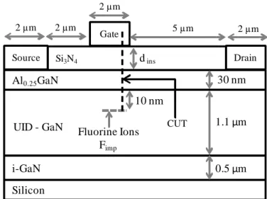
Chapter 3 A normally-off HEMT with Fluorine implantation below the channel ... 53
3.1. Introduction ... 55
3.2. HEMT with Fluorine implanted below the channel ... 55
3.2.1. Fluorine implantation below the channel ... 55
3.2.2. Comparison between implantation in the barrier layer and implantation below the channel ... 57
3.2.3. Variations of the threshold voltage with the distance "d" ... 58
3.2.4. Breakdown voltage and off-state current ... 61
3.2.5. Forward gate voltage ... 62
3.3. MIS-HEMT with Fluorine below the channel ... 62
3.3.1. Effect of Fluorine concentration ... 63
3.3.2. Variation of the threshold voltage with thickness of the insulator ... 66
3.3.3. Variations with the permittivity of the insulator ... 67
3.4. Effect on the transconductance ... 69
3.5. AlN interlayer for better transconductance ... 71
Chapter 4 A normally-off HEMT with a buried p-GaN region ... 75
4.1. Introduction ... 77
4.2. HEMT with buried p-region ... 77
4.2.1. Effect of the width of the p-region Pw ... 79
4.2.2. Effect of the thickness of the p-region Pth ... 80
4.2.3. Effect of x-mole fraction: decreasing the download push of the triangular well ... 83
4.2.4. Effect of p-doping concentration ... 84
4.2.5. Effect of the distance "d" between p-region and the AlGaN/GaN interface ... 86
4.3. MIS-HEMT with a buried p-region ... 87
4.3.1. Variation with doping concentration ... 88
4.3.2. Variations of the threshold voltage with thickness of the insulator ... 89
4.3.3. Variations with the permittivity of the insulator ... 89
4.4. Comparison between the HEMT with a buried p-region and the Gate Injection Transistor (GIT) ... 92
4.4.1. Gate Injection Transistor ... 92
4.4.2. HEMT with a buried p-region versus GIT ... 93
4.4.3. Hybrid normally-off GIT with a buried p-region ... 95
4.5. New structures easing the fabrication of normally-off HEMTs with a buried p-region ... 98
4.5.1. Structure #1 ... 98
4.5.1.1. Device design and fabrication process ... 98
4.5.1.2. Conditions for operation ... 99
4.5.1.3. Band diagram ... 101
4.5.1.4. Sensitivity analysis ... 102
4.5.2. Structure #2 ... 105
4.5.2.1. Device design and fabrication process ... 105
4.5.2.2. Sensitivity analysis ... 106
Chapter 5 General conclusion and future work ... 109
5.1. General conclusion ... 111
5.2. Future work ... 113
5.2.1. Structure for fabrication ... 113
5.2.2. Develop and implement a new mobility model ... 113
5.2.3. Linking the equivalent interfacial charge to the Gaussian profile ... 114
5.2.4. AC and transient analysis ... 114
Abstract
AlGaN/GaN HEMTs are very promising candidates for high frequency applications with high power and low noise. While switching applications strongly demand normally-off operation, conventional HEMTs attain a channel populated with electrons at zero gate voltage making them normally-on. For the sake of achieving normally-off HEMTs, several structures have been proposed such as recessed gate structures, Fluorine ion treatment, P-GaN gate structures, thin AlGaN barrier and Gate Injection transistor.
The effectiveness of the agent used to obtain normally-off, whether it is recessing the gate, introducing a cap layer or implanting Fluorine, increases as the agent comes closer to the AlGaN/GaN interface. Unfortunately, when introducing a cap layer or recessing the gate, coming closer to the interface means decreasing the barrier thickness, which strongly affects the density of the 2DEG. In the case of Fluorine implantation, getting closer will increase the probability of Fluorine ions getting into the channel and hence degrade the mobility of the 2DEG.
In this work we propose two new concepts to achieve normally-off operation. We suggest the introduction of negative Fluorine ions on one hand or a p-GaN region on the other hand, below the channel, under the AlGaN/GaN interface and away from high current density regions. After calibrating the simulator using experimental results from a normally-on HEMT device, we will show that our proposed structures are more effective: the concentration required to achieve normally-off operation is lower than in the other existing solutions, and the confinement of the two dimensional electron gas below the gate is better.
The proposed ideas were also applied to Metal Insulator Semiconductor HEMT (MIS-HEMT) and Gate Injection Transistor (GIT), giving rise to a normally-off HEMT with high controllable threshold voltage.
Acknowledgments
This research would not have been possible without the guidance and the help of several individuals who in one way or another contributed and extended their valuable assistance in the preparation and completion of this study.
In the first place, I would like to record my gratitude to my advisors Prof. Bilal Beydoun and Prof. Frédéric Morancho for their supervision, advice, extraordinary patience and guidance from the very early stage of this research.
To Danial, Saleh, Amin, Bahaa, Haytham, Taher, Wisam, Osama, Jamal, Amin and Alaa, thank you for your thoughts, prayers, phone calls, e-mails, texts, visits and being there whenever I needed a friend. You all are the best friends anyone could ever ask for.
To Hadi, thanks for listening, offering me advice, and supporting me through this entire process.
Thanks to Dr. Yehya Amer for his endless support, care and encouragement
Special thanks for my friends at LAAS, Housam, Nadim, Serge, Ayyad and Mostapha. The debates, dinners, rides to the airport, and general help and friendship were all greatly appreciated.
I am grateful to all the administrative staff at the Lebanese and Paul Sabatier Universities and at the LAAS laboratory, for the practical support throughout my PhD, including, Ms. Camille Cazeneuve, Ms. Marie-Thérèse Funch, Ms. Claire Bardet, Ms. Zeinabou Sabatier, Ms. Ascension De Sousa, Ms. Isabelle Izarié and Ms. Zeinab Ibrahim.
To Mr Denis Griot and Prof. Augustin Martinez, thanks for the friday meetings, for giving me insight on the market of GaN and for believing in my potential.
My thanks go to my thesis reporters, Prof. Yvon Cordier and Prof. Clovis Francis and for the jury members for their comments and remarks.
I would like to extend my gratitude to the Azm and Saada association and for the LAAS laboratory for financing this research project.
Words fail me to express my appreciation to my parents, Yousef and Aida Hamady for their love and support. My life has been extremely blessed to have two wonderful, loving parents whose love and support of anything I do has never been in doubt. To my brothers Faisal and Kareem and to my sister Hind thanks for all the emotional support, loving entertainment, and caring. I thank god for my family to whom I dedicate this thesis.
Saleem HAMADY
List of Acronyms
2DEG Two dimensional electron gas
AC Alternating current
AlGaN Aluminum Gallium Nitride
DC Direct current
GaN Gallium Nitride
GIT Gate injection transistor
Grid T&D Grid Transmission & Distribution GTO Gate turn-off thyristor
HEMT High electron mobility transistor
HVAC Heating, ventilation, and air conditioning HVDC High voltage direct current
IGBT Insulated gate bipolar transistor
MOSFET Metal insulator semiconductor field effect transistor
Si Silicon
SiC Silicon Carbide
UPS Uninterruptible power supply
Electronic devices have truly blended in with our lives and expand our capabilities and potential. Development and innovation in this field will shape the future of mankind. In the electronic devices we use today, solid-state devices are utilized to control or convert electric power into different forms. This domain is known as power electronics. In our smart phones, tablets, PDAs and almost every mobile device, a DC/DC converter is used to maintain a fixed output voltage regardless of the battery voltage level. Most of the electronic devices connected to the mains (laptops, TVs, etc) utilize an AC/DC converter, which are also known as rectifiers. DC/AC converters, also known as inverters, are used in hybrid vehicles, renewable energy systems, UPS and emergency lighting systems. After storing AC voltage in DC batteries, the batteries can later be used to generate AC voltage with the help of an inverter. AC/AC converters are found in international power adapters, light dimmer, fan with controllable speeds and many other applications that require a change in the frequency or voltage level of an AC signal.
Improving the efficiency of power electronic devices is crucial to reduce switching losses and hence lower the CO2 emission. Today, the vast majority of power devices are made from
silicon. Unfortunately, the intrinsic physical properties of silicon set a theoretical limit on the capabilities of silicon power devices hindering them, in some domains, from being the candidates for future power electronics. With silicon power devices reaching their theoretical limits, design engineers are facing the challenge of increasing the ratings of converters in terms of operating voltage, operating temperature and efficiency. The quest for a solution to silicon limitations leads researchers to the doorstep of wide bandgap materials such as Silicon Carbide (SiC) and Gallium nitride (GaN). Compared to silicon, the main benefits of these materials are a good operation over a wide temperature range, high critical electric field and high saturation velocity.
SiC power components have been a subject of extensive research in the past fifteen years. However, despite the remarkable results obtained by several teams, SiC must be grown on native substrates which are expensive and relatively small in size (100 mm in diameter). On the other hand, GaN can be grown on silicon substrates which are of low cost and large size (150 to 200 mm in diameter). Moreover, GaN is better than SiC for creating heterostructures due to their built-in polarization field. Therefore, for devices such as HEMT, GaN is the material of choice.
The polarization doped High Electron Mobility Transistor (HEMT) is a field effect transistor in which two layers of different bandgap and polarization field are grown upon each other. As
a consequence of the discontinuity in the polarization field, surface charges at the heterointerface are created. If the induced charge is positive, electrons will tend to compensate the induced charge resulting in the formation of the channel. Since in the HEMT the channel electrons are confined in a quantum well in a very narrow spatial region at the heterointerface, the channel electrons are referred to as a Two Dimensional Electron Gas (2DEG). This confinement grants the electrons high mobilities surpassing the bulk mobility of the material in which the electrons are flowing. Thanks to the GaN properties and the HEMT’s topology, AlGaN/GaN HEMTs are now promising devices for high frequency applications with high power and low noise, such as microwave and millimeter wave communications, imaging and radars.
While power switching applications strongly demand normally-off operation with a threshold voltage above 3V, conventional HEMTs attain a channel populated with electrons at zero gate voltage making them normally-on. Several normally-off structures have been proposed such as recessed gate structures, fluorine ion treatment, P-GaN gate structures, thin AlGaN barrier and the Gate Injection Transistor. The effectiveness of the agent used to obtain normally-off, whether it is recessing the gate, introducing a cap layer or implanting fluorine, increases as the agent comes closer to the AlGaN/GaN interface. Unfortunately, in introducing a cap layer or recessing the gate, coming closer to the interface means decreasing the barrier thickness, which strongly affects the density of the 2DEG. In the case of fluorine implantation, getting closer to the interface increases the probability of fluorine ions getting into the channel and hence the degradation of the mobility of the 2DEG.
In this work, two new normally-off concepts are proposed. To examine their electric characteristics, a commercial TCAD simulation tool from Silvaco is used. Technology Computer Aided Design (TCAD) tools are simulation tools used to model the processing and behavior of electronic devices. The simulator can predict the electrical behavior of semiconductor devices at specified bias conditions.
After introducing the structure, composition and features of the conventional HEMT in chapter 1, the device simulator is explained in chapter 2 showing the input to the simulator, the fitting strategy and the models used. In chapters 3 and 4, the two new normally-off designs are shown along with the results of the sensitivity analysis for the HEMT with Fluorine implanted below the channel and HEMT with buried p-region respectively.
Chapter 1
1.1. Introduction
The reduction of CO2 emission has always been a subject of extensive research. In the
domain of power electronics, the reduction of CO2 emission can be achieved by increasing
the efficiency of power converters by reducing the switching losses in power devices [1]. Today, the vast majority of power devices are made from silicon. Unfortunately, silicon is reaching its theoretical limit in terms of device performance. The quest for a solution to silicon limitations leads researchers to the doorstep of wide bandgap materials, such as Silicon Carbide (SiC) and Gallium nitride. When compared to SiC, GaN is a better candidate to fabricate heterostrucutres and, unlike SiC, can be grown on silicon substrates. This chapter shows the fundaments of the HEMT device fabricated using GaN based materials. Afterwards, the state of the art normally-off HEMT structures are explained and shown. 1.2. Power devices
For ultimate efficiency in power conversion, an ideal switch is required. An ideal switch has zero voltage drop and no limit on the current level carried during the on-state. During the off-state, it attains infinite resistance (zero leakage current) and can sustain unlimited voltages. The time to switch between the on and off-state is zero [2].
The quest for the ideal switch results in the development of various power components, each resembles in a way a characteristic of the ideal switch. In practical switches, there is a trade-off between voltage, current and frequency ratings.
1.2.1. Silicon power devices
Figure 2 shows the split of the main power devices depending on their current, voltage and frequency rating. The power MOSFETs are found in applications demanding small inverters (Watt to kW range) such as VTRs, mobile phones, communication devices, audio equipments and many others.
The IGBT performance is regularly improving as technology evolves and has already replaced the bipolar transistor in power applications. Moreover, IGBT power modules, parallelly combining several IGBT devices, are attractive for power levels up to several Megawatts. The operating frequency of the IGBT is relatively low mainly because of a problem during turn-off known as current-tail. IGBTs and IGBT modules are utilized in applications using inverters with a switching power ranging from kW to MW such as air conditioners, refrigerators, railways, paper making, etc.
Thyristor-based devices are the only choice at very high power. The problem with thyristors is that once it starts conducting, the gate loses its control over the device. To solve this problem, the gate turn-off thyristor (GTO) was later introduced which is a fully controllable switch that can be turned on and off. However, while thyristors are used in medium to high voltage applications, GTO are used at medium voltages only. Thyristors and thyristor-based devices are used in AC drives, HVDC and Grid T&D [3].
It is worth mentioning that recent improvements of Si devices (superjunction, high speed IGBT) and the introduction of new materials (SiC, GaN) will mix the performance and open new device choices. For instance, GaN on Silicon devices are expected to be faster than IGBTs and more powerful than MOSFETs. GaN-based power solutions are expected to increase efficiency, reduce system size, and simplify overall product design and can eliminate up to 90% of all electric conversion losses from heating, ventilation, and air-conditioning systems (HVAC). Therefore GaN power devices are expected to replace silicon MOSFETS and IGBT modules in applications like VTRs, communication devices, audio equipments, AC adapters and electric/hybrid vehicles [3].
Figure 1.1 Classification of the main power devices according to their switching frequency, voltage and current ratings
Frequency
Frequency New expected capabilities offered by GaN-‐on-‐Si devices
1.3. Theoretical limits for power devices
When increasing the applied voltage across a power device, the electric field within the device begins to increase. Once the electric field approaches a critical level Ec, the power
device tends to undergo avalanche breakdown. To allow simple comparison between similar systems with different material compositions, an abrupt one-dimensional P+/N diode is studied [4]. In this study, it is assumed that the voltage is supported across only one side of the structure. This assumption holds true for an abrupt P+N junction since the doping concentration on one side is very high compared to the other. Moreover, since the P+ region is taken very thin and highly doped compared to the n-region, the depletion region extends primarily in the N-doped region [4].
When this diode is reverse biased, a depletion region is formed in the N-region (the depletion in the P+ region can be neglected). The electric field in the depletion region can be extracted from the Poisson's equation:
∇!𝑉 = −𝜌
𝜀! (1.1) 𝐸 = −∇. 𝑉 (1.2) where V is the electrostatic potential, 𝜌 is the charge density, 𝜀! is the dielectric constant of the semiconductor and E is the electric field.
Figure 1.2. Schematic cross-section of an abrupt P+N junction showing the electric field distribution inside the depletion region when the junction is reversed biased
P+
Depletion region NP+
N WD E x EmIn our case (one dimensional case): 𝑑!𝑉 𝑑𝑥! = − 𝑑𝐸 𝑑𝑥 = − 𝜌 𝜀! = − 𝑞𝑁! 𝜀! (1.3) The charge within the depletion region due to the presence of ionized donors can be expressed as 𝑞𝑁!, q is the proton charge and ND is the donor concentration in the uniformly
doped N-region. The solution of equation 1.3, with the use of the boundary conditions 𝐸 𝑊! = 0 and 𝑉 0 = 0, yields the following expressions for the electric field and the electrostatic potential: 𝐸 𝑥 = −𝑞𝑁! 𝜀! 𝑊!− 𝑥 (1.4) 𝑉 𝑥 =𝑞𝑁! 𝜀! 𝑊!𝑥 − 𝑥! 2 (1.5) 𝑊! can be related to the applied voltage by using the condition 𝑉 𝑊! = 𝑉! , where 𝑉! is the applied reverse voltage.
𝑊! = 2𝜀!𝑉! 𝑞𝑁! (1.6) At breakdown 𝑉! = 𝑉!" and 𝐸! = 𝐸(0) = 𝐸! 𝑊! = 2𝜀!𝑉!" 𝑞𝑁! (1.7) 𝐸! = −𝑞𝑁! 𝜀! 𝑊! ⇒ 𝑊! = −𝜀! 𝐸! 𝑞𝑁! (1.8) Combining equations 1.7 and 1.8, we get:
𝑁! = 𝜀! 𝐸!
!
2𝑞𝑉!" (1.9) 𝑊! = 2𝑉!"
𝐸! (1.10) The specific on resistance per unit area of the ideal uniformly doped drift region is:
𝑅!",!" = 𝑊!
𝑅!",!" = 4 𝑉!"
𝜀!𝜇!𝐸!! (1.12)
The denominator of this equation (𝜀!𝜇!𝐸!!) is commonly referred to as Baliga’s figure of
merit for power devices [5]. It is an indicator of the impact of the semiconductor material properties on the resistance of the drift region. An accurate modeling of the specific on resistance requires taking into account the dependence of the critical electric field and mobility on the doping concentration.
Practical specific ON-resistance estimation is calculated using the following approximation [6]: 𝐸! ∝ 𝑁!! 𝜇! ∝ 𝑁!!! 𝑅!"(Ω. 𝑐𝑚!) ∝ 𝑉 !"! 𝜂 = 2 − 𝑥 − 𝑦 1 − 2𝑦 For Si [4]:𝑅!" Ω. 𝑐𝑚! = 5.93 ×10!! 𝑉 !"!.! (1.13) For 4H-SiC [4]: 𝑅!"(Ω. 𝑐𝑚!) = 2.97 ×10!!" 𝑉 !"!.! (1.14)
Figure 1.3. Theoretical on-resistance versus breakdown voltage for different materials showing an advantage for wide bandgap semiconductors [5]
For 6H-SiC [7]: 𝑅!"(Ω. 𝑐𝑚!) = 1.45 ×10!!! 𝑉
!"!.! (1.15)
For GaN [7]: 𝑅!" Ω. 𝑐𝑚! = 2.4 ×10!!" 𝑉!"!.! (1.16)
Figure 1.3 shows the plot of equations 1.13, 1.14, 1.15 and 1.16 [5]. It is clear that the theoretical limit of wide bandgap materials is much higher than that of silicon. This means that, for the same breakdown voltage, devices based on wide bandgap materials offer a significantly lower ON-resistance.
1.4. Wide bandgap power devices
With silicon power devices reaching their theoretical limits in terms of temperature and power operation, design engineers are facing the challenge of increasing the ratings of converters in terms of operating voltage, operating temperature and efficiency. The quest for a solution to silicon limitations leads researchers to the doorstep of wide bandgap materials such as Silicon Carbide (SiC) and Gallium Nitride (GaN).
Wide bandgap materials show superior advantages over silicon such as large bandgap, high critical breakdown field strength and high thermal conductivity in some cases (SiC). The values are illustrated in table 1. The translation of these superior physical properties to the devices is shown in figure 1.4. The high critical electric field and the wide energy gap enable operation at high voltages and elevated temperatures. The high switching frequency is attributed to the high saturation electron velocity and high mobilities. From figure 1.4, it can be concluded that SiC will stay the preferred choice for high temperature applications. GaN has an extra advantage compared with SiC as a result of the enhanced mobility of electrons in the two dimensional electron gas (2DEG). This translates into a GaN device with a smaller size for a given on-resistance and breakdown voltage.
Item Unit Si 4H-SiC GaN
Band gap eV 1.1 3.26 3.4
Electron mobility cm2/V.s 1300 900 900 - 2000
Breakdown field strength V/cm 0.3 ×10⁶ 3 × 10⁶ 3.5 × 10⁶ Saturated electron speed cm/s 1 × 10⁷ 2 × 10⁷ 2.5 × 10⁷
Thermal conductivity W/cm.K 1.5 3.7 1.3
Table 1 Physical properties of Silicon (Si), Silicon Carbide (4H-SiC) and Gallium Nitride (GaN)
The applications for various power devices along with the material capabilities are shown in figure 1.5 [3]. It is clear that high power and high frequency applications are demanding more than silicon can offer. SiC is expected to cover the high power low frequency applications while GaN covers the high frequency relatively low power applications. The competition between SiC and GaN will be at intermediate frequencies and moderate power.
Figure 1.4 Comparison between Silicon, Gallium Nitride and Silicon Carbide based on their physical properties
Figure 1.5 Applications for various power devices along with the material capabilities [3]
1.5. Gallium Nitride (GaN)
1.5.1. Gallium Nitride physical properties
Gallium Nitride (GaN) is a semiconductor material belonging to the III-V semiconductor family. Its crystal structure may differ between Wurtzite and Zinc blend. The two structures are shown in figure 1.6 [8]. Since AlGaN/GaN HEMTs are grown on the Wurtzite phase, only this crystal structure will be further explained. The unit cell of the III-N Wurtzite structure is the hexagonal cell consisting of two intercepting Hexagonal Closed Packed (HCP) sub-lattices, each formed by one type of atoms. The structure is fully defined by three lattice constants: the side's length of the hexagonal base "a", the height of the cell "c" and the shift, along the c-axis, between the 2 sub-lattices "u". In an ideal Wurtzite structure, when atoms are considered to be touching hard spheres, the ratio of these parameters is 𝑐! 𝑎! = 8 3 = 1.633 and 𝑢! 𝑐! = 3 8 = 0.375. GaN can be doped with silicon (Si) or with oxygen to n-type [9] and with magnesium (Mg) to p-type [10].
Beside the advantage of Wurtzite structure being favored at room temperature due to its stability, it possesses a built-in polarization field named the spontaneous polarization Psp.
This field springs up due to the ionic nature of the gallium-nitrogen bond and the lack of inversion symmetry within some planes within the crystal. The values of the spontaneous polarization of some binary and trinary III-N alloys is shown in figure 1.7 [11].
(a) (b)
Figure 1.6 Crystal structure of GaN (a) Zinc blend and (b) Wurtzite structure [8]
a c
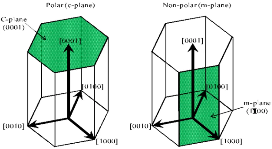
Planes lacking inversion symmetry will attain a polarization field along their normal vector. In Wurtzite GaN (w-GaN), the (0001) plane, named the c-plane, attains spontaneous polarization, while the (1100) and (1120) planes, named m- and a-planes respectively, do not. Some of the polar and non-polar planes are shown in figure 1.8.
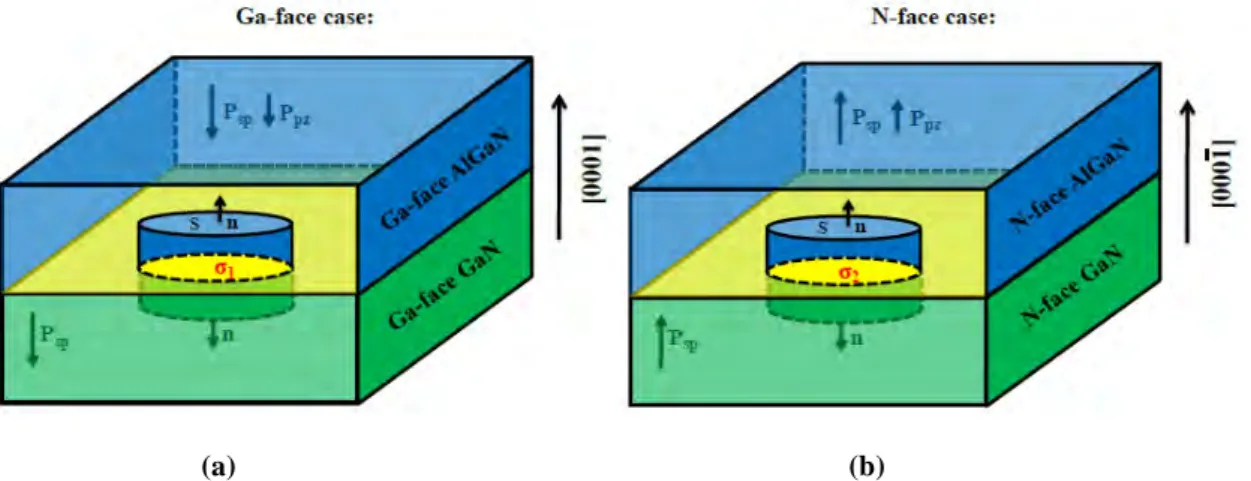
In order to take advantage of the spontaneous polarization, GaN is grown perpendicularly to the c-plane. The resulting surface is either the (0001) also known as Ga-faced or (0001)
Figure 1.7. Spontaneous polarization of III-N binary and ternary alloys. The thin lines show linear interpolation while the thick ones show second order approximation [11]
AlN InN GaN 0 -0.02 -0.04 -0.06 -0.08 -0.1 0.3 0.31 0.32 0.33 0.34 0.35 0.36 0.37 S p o n ta n eo u s p o la ri za ti o n ( C /m 2) Lattice Constant a (nm)
Figure 1.8 To the left the polar plane known as c-plane (0001) and to the right a non-polar plane (𝟏𝟏𝟎𝟎) known as the m-plane
known as N-faced. The orientation of the polarized field in N-faced plane is opposite to that in the G-faced. Distinction between these two orientations can be done by variety of techniques including wet chemical etching, characterization of physical morphology, and convergent beam electron diffraction [12]. The atomic arrangement in GaN-face and N-face GaN is shown in figure 1.9 [13]
1.5.2. Elastic and piezoelectric properties
In addition to the spontaneous polarization, GaN as well as GaN alloys possess piezoelectric properties. When an external electric field is applied to piezoelectric materials, they mechanically deform. Conversely, these materials generate an electric field in response to an applied mechanical stress/strain. When growing two materials with different lattice constant upon one another, at certain conditions discussed in 1.4.3.3, the above layer will stretch or shrink so that its lattice constant matches the layer upon which it is grown. This stretch/strain will generate a polarization field named piezoelectric polarization 𝑃!".
The piezoelectric polarization is simply expressed as:
𝑃!" = 𝑒!!𝜀! + 𝑒!". 𝜀!+ 𝜀! (1.17) where: 𝜀! = 𝜀! = 𝑎 − 𝑎! 𝑎! , 𝜀! = 𝑐 − 𝑐! 𝑐! (1.18) and: 𝜀! = −2 𝐶!" 𝐶!! 𝜀! (1.19)
Figure 1.9 Atomic arrangement in Ga-face and N-face GaN [14]
𝑎! and 𝑐! are the equilibrium value of the lattice constant (base material), 𝑎 and 𝑐 are the lattice constants of the material that is to be deposited (stretched or strained material), 𝑒!! and 𝑒!" are piezoelectric coefficients, 𝐶!! and 𝐶!" are elastic constants, 𝜀! is the strain along
the c axis, 𝜀! and 𝜀! are the in-plane strains that are assumed to be isotropic. Hence 𝑃!" can be written as: 𝑃!" = 2 𝑎 − 𝑎! 𝑎! 𝑒!"− 𝑒!! 𝐶!" 𝐶!! (1.20) 1.6. Bound charge
When two layers with different polarization fields are grown upon one another, a bound charge at their interface will be created. Depending on the divergence of the polarization field, this charge can be positive or negative. The bound charge can be calculated using the following equation:
𝜌! = −∇. 𝐏 (1.21) where 𝜌! is the bound charge density and P is the polarization field.
Figure 1.10 shows the bound charge created at the interface of AlGaN/GaN in two different cases. The GaN layer is assumed to be relaxed and hence attains only spontaneous polarization. On the other hand, the AlGaN layer is strained and therefore attains both spontaneous and piezoelectric polarizations.
The sign of the bound charge is derived from equation 1.21. Figure 1.11 shows a detailed derivation of the bound charge.
Figure 1.10 Bound charge at the AlGaN/GaN interface for (left) Ga-face and (right) N-Face
We have from equation 1.21:
∇. 𝑷 = −𝜌! Integrating on both sides, we get:
∇. 𝑷 𝑑𝑣 = − 𝜌! 𝑑𝑣 (1.22)
𝜌! 𝑑𝑣 = 𝑄! (1.23) where 𝑄! is the bound charge at the interface.
Using divergence theorem and equation 1.23 we get:
𝑷. 𝑑𝑺 = ( 𝑷. 𝒏 ) 𝑑𝑆 = −𝑄! (1.24) A cylindrical closed surface is chosen as shown in figure 1.11.
𝒏 is the vector perpendicular to the surface of the cylindrical closed surfaces.
In the case of growing in the [0001] direction figure 1.11 (a), the resulting bound charge is positive. ( 𝑷. 𝒏 ) 𝑑𝑆 = −𝑄! ⟹ − 𝑃!"#$%𝑆 + 𝑃!"#𝑆 = −𝑄! ⟹ 𝑃!"#$%− 𝑃!"# = 𝑄! 𝑆 = 𝜎! 𝑃!"#$% > 𝑃!"# ⟹ 𝜎! > 0 (a) (b)
Figure 1.11 A cylindrical closed surface is used to solve equation 1.23 to calculate the bound charge the interface in (a) Ga-face AlGaN on top of Ga-face GaN and in (b) N-face AlGaN on
top of N-face GaN
In the case of growing in the [0001] direction (figure 1.11 (b)), the resulting bound charge is negative. 𝑷. 𝒏 𝑑𝑆 = −𝑄! ⟹ 𝑃!"#$%𝑆 − 𝑃!"#𝑆 = −𝑄! ⟹ 𝑃!!"− 𝑃!"#$% = 𝑄! 𝑆 = 𝜎! 𝑃!"#$% > 𝑃!"# ⟹ 𝜎! < 0
A third configuration can be used to increase the divergence in the polarization field and hence increase the density of bound charge at the interface. If a Ga-face AlGaN layer is grown on top an N-face GaN layer (figure 1.12) the resulting bound charge would be:
𝑷. 𝒏 𝑑𝑆 = −𝑄! ⟹ − 𝑃!"#$%𝑆 − 𝑃!"#𝑆 = −𝑄! ⟹ 𝑃!"#$%+ 𝑃!"# =𝑄!
𝑆 = 𝜎! > 0
To numerically compare 𝜎! to 𝜎! , the x-mole fraction in the AlGaN is taken 0.25. For the case of Ga-face AlGaN / Ga-Face GaN:
𝜎! = 5.1 ×10!!− 2.9×10!!= 2.2×10!! 𝐶
𝑐𝑚!
For the case of Ga-face AlGaN / N-Face GaN:
𝜎! = 5.1 ×10!!+ 2.9×10!!= 8×10!! 𝐶 𝑐𝑚! σ! σ! = 3.63
Figure 1.12 A cylindrical closed surface is used to solve equation 1.23 to calculate the bound charge at Ga-face AlGaN / N-face GaN interface
n Psp Ppz Psp n S σ3 [000 1] [000 1]
Although this approach may theoretically results in a much higher bound charge, it will introduce a large number of defects at the AlGaN/GaN interface making it useless.
1.7. AlGaN/GaN High electron mobility transistor 1.7.1. Basic structure
The high electron mobility transistor (HEMT) is a field effect transistor in which two layers of different bandgaps and polarization fields are grown upon one another. As a consequence of the discontinuity in the polarization field, surface charges at the heterointerface are created. If the induced charge is positive, electrons will tend to compensate the induced charge resulting in the formation of a two dimensional electron gas (2DEG). The 2DEG represents the channel of the HEMT and the current flow between the drain and the source is controlled by the gate of the device. The schematic cross-section of the conventional HEMT is shown in figure 1.13
The substrate is used as the base for the growing process. HEMTs are currently grown on Silicon [14][15][16][17], sapphire [18][19][20], Silicon Carbide [21][22][23] and GaN substrates [24]. Figure 1.14 [3] compares the four substrates according to the available size, cost, thermal conductivity, difference in heat expansion and lattice constant when compared to Gallium Nitride [3]. Silicon Carbide and sapphire substrates were the first to be studied, benefiting from the existing experience and tool sets in the LED industry. However, the successful growth of GaN on Silicon attracts the industry because of the availability of large silicon wafers at low cost. Currently the best results, which are obtained on SiC substrates, are likely reproduced by using Silicon substrates.
Figure 1.13 Schematic cross-section of the conventional high electron mobility transisitor (HEMT)
As for the GaN substrates, although there is no lattice mismatch problem, these substrates remain undesirable because of their small size and extreme high cost.
Nucleation buffer layers: When GaN is grown on foreign substrates (except for saphire), due to the lattice mismatch, a tensile strain arises favoring the creation of cracks. To prevent this cracking, intermediate layers are introduced between the substrate and the channel layer to compensate for the significant lattice mismatch between GaN and the substrate.
Channel layer: On the buffer layer a GaN layer is grown mostly along the [0001] direction to benefit from the spontaneous polarization of the c-plane within the GaN Wurtzite crystal. Within this layer the channel will be formed, hence, it is sometimes referred to as the channel layer.
Barrier layer: On top of the channel layer, a layer with higher bandgap and lesser electron affinity is grown. Due to the conduction band offset and the difference in the polarization between the barrier and the channel layer, a potential quantum well will be created underneath the hetero-interface, trapping the electrons inside, and consequently creating the channel. The depth of the well is associated with the difference of electron affinity. In GaN HEMTs, AlGaN is usually used as a barrier layer. The barrier layer can be either doped or intrinsic. In GaAs HEMTs, since the barrier layer is doped, a thin intrinsic layer known as spacer layer, with the same material as the barrier, is introduced between the channel and the barrier to prevent ionized impurity scattering between the electrons in the channel and the dopant atoms [25]. In GaN HEMTs, an interlayer of AlN [26] is sometimes used to enhance the confinement of the channel electrons and increase their density.
Figure 1.14 Comparison between different substrates on which GaN can be grown [3]
Passivation layer: it is usually SiN, which reduces the response of the surface traps which in return suppress the effect of current collapse [27].
Electrodes, named the source and the drain, are placed on highly doped semiconductor to achieve ohmic contacts. However, the third electrode, named the gate, is placed on non-heavily doped semiconductor to generate the Schottky barrier. The Schottky gate controls the carrier concentration in the channel layer below the interface. As the gate voltage decreases, the carrier concentration below the gate electrode decreases. The gate bias required to pinch-off the channel is called the threshold voltage (Vth). Below Vth, channel becomes
depleted from carriers, and thus, no current can flow between the drain and source. When the threshold voltage is negative, the HEMT is called a depletion-mode (D-mode) HEMT or normally-on and, when it is positive the device is then called an enhancement-mode (E-mode) HEMT or normally-off. Conventional AlGaN/GaN HEMTs are D-mode transistors.
1.7.2. Band diagram of conventional HEMTs
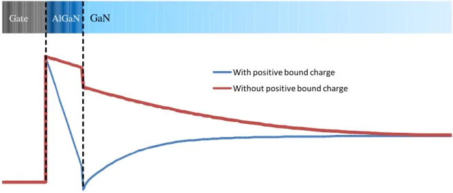
To understand the behavior of the HEMT, one must understand the variation of the energy band diagram with the applied voltage. If an AlGaN layer is grown on a GaN layer, assuming no positive bound charge at their interface due to the discontinuity of the polarization field, the band diagram looks like the illustration in figure 1.15.
To draw this figure no built-in potential is assumed and hence the Vacuum level is drawn first. Afterwards, knowing that the difference between the conduction band and the Fermi
Figure 1.15 Band diagram of an AlGaN/GaN hetero-structure without the consideration of the positive bound charge at the AlGaN/GaN interface
Vacuum Level Conduction Band Ec Valence Band EV Fermi Level EF ? Ec ? EV Eg, AlGa N Eg, Ga N
?
AlGa N?
Ga N AlGaN GaNlevel is equal to the electron affinity χ of the material, the conduction band is drawn. Then from the conduction band, by knowing the bandgap of the material, the valence band can be located. The Fermi level, at equilibrium, must be constant throughout the layers. In figure 1.15, we have assumed, to reduce complexity, that the Fermi level is pre-aligned before enforcing equilibrium conditions. However, in real cases, a constant Fermi level must be drawn first, then the conduction and valence bands, and finally the Vacuum level. The position of the conduction band with respect to the constant Fermi level is separately drawn in each region according to the doping concentration. In n-doped semiconductors, the Fermi level is higher than that of the intrinsic semiconductor and lies closer to the conduction band. On the other hand, in p-doped semiconductors, the Fermi level is lower than that of the intrinsic semiconductor and lies closer to the valence band. The severity of the shift of the Fermi level from the intrinsic level depends on the doping concentration. As the doping concentration increases, the shift from the intrinsic level increases.
The conduction band offset, known as ΔEc, can be extracted from the difference of the
electron affinity of the two layers.
∆𝐸! = 𝜒!"#− 𝜒!"#$% (1.25) The conduction band offsets changes from 74% to 72% of ∆𝐸! with increasing Al content in an AlGaN/GaN system [28].
In fact, conventional AlGaN/GaN HEMTs have a Schottky gate contact and a positive bound charge at the AlGaN/GaN interface. These two factors strongly affect the band diagram. The domain of interest in HEMT transistors is at the hetero-interface (AlGaN/GaN interface), Hence, the study will be focused on that region. The schematic cross-section of a normally-on HEMT and an illustration of its band diagram are shown in figure 1.16. The first important point is that the conduction band at the Gate/AlGaN interface is pinned to the Schottky barrier Φ!which can be calculated as:
Φ! = 𝑊!− 𝜒!"#$% (1.26) where 𝑊! is the workfunction of the metal and 𝜒!"#$% is the electron affinity of AlGaN. The second important point is the impact of the bound charge on the band diagram. In figure 1.15, the conduction band is above the Fermi level throughout the two layers. However, when positive bound charge is added at the AlGaN/GaN interface, the conduction band at the interface bends. As the charge concentration increases, the bending increases. This bending,
if high enough, will cause part of the conduction band in the vicinity of the interface to go below the Fermi level.
In that region (Fermi level above the conduction band) electrons will populate on the energy levels of the triangular quantum well formed at the AlGaN/GaN interface. These electrons form the HEMT's channel and are known as the Two Dimensional Electron Gas (2DEG).
Figure 1.16 Schematic band diagram of a conventional normally-on HEMT. At the gate/AlGaN interface, the conduction band energy is equal to the Schottky barrier. The positive bound charge
at the AlGaN/GaN interface bends the conduction band causing the creation of the triangular well. Electrons occupying the energy levels of the triangular well form the HEMT's channel
Conduction band Ec Fermi level EF S our ce Dr ai n Ga te Triangular quantum well (TQW) Energy level of the QW G aN A lG aN Depth En e rg y + + + + + + + + + + + + + + + + + + + + + + + + + + + + P os it ive b ou n d ch ar ge T w o d im e n si onal el ec tr on gas ( 2D E G ) G aN A lG aN e e e e e e e e C h an n el el ec tr on s fr om th e 2D E G S chot tky ba rr ie r ɸB G at e Δ Ec
Figure 1.17 Variations of the electron mobility versus temperature for 2DEG in Al0.1GaN/GaN and
for bulk n-GaN with ND = 10 17
The confinement of the channel electrons in the quantum well grants them two-dimensional features, which strongly enhance their mobility. Figure 1.17 [29] shows the variation of the electron mobility versus temperature for 2DEG in Al0.1GaN/GaN and for bulk n-GaN with
an n-doping concentration 1017 cm-3. It is clear that the mobility of the 2DEG is higher at all temperatures.
To manipulate the density of electrons in the channel, and hence switch the HEMT ON and OFF, the voltage at the gate is varied. Here, it is worth defining the threshold voltage Vth as
the voltage required to populate electrons at the interface and hence giving the channel conduction privilege. Figure 1.18 shows the triangular quantum well at three different biasing conditions.
Channel electrons occupy energy levels that are positioned below the Fermi level. When the gate voltage is much higher than the threshold voltage (Vgs >> Vth), the Fermi level in the
triangular well is above several energy levels. This enables high population of channel
Figure 1.18 Position of the Fermi level with respect to the conduction band at various biasing conditions. The zoomed parts illustrate the status of the triangular well at the AlGaN/GaN interface to show the depletion of channel electrons (2DEG) as the gate voltage goes below the
threshold voltage GaN AlGaN Gate Vg> 0 > Vth Vg= 0 > Vth 0 > Vth> Vg qVg qVg e e e e e e e e e e Fermi Level Conduction band Energy Level
electrons and hence high current density. When the gate voltage decreases, the Fermi level goes downwards with respect to the triangular well. Therefore fewer energy levels are populated and hence the concentration of channel electrons, below the gate, decreases. Once the gate voltage goes below the threshold voltage, all energy levels are above the Fermi level. This causes channel depletion and the HEMT turns OFF.
1.7.3. Source of the 2DEG
Surface traps are energy states in the band-gap of a semiconductor. They originate from factors such as crystal defects, dislocations, or the presence of impurities. Classification of these traps depends on the relative position of their energy level inside the band gap. Traps with energy above the Fermi level are acceptor-like, attaining negative charge when occupied. However, traps with energy below the Fermi level are donor-like, positively charged when empty and neutral when occupied.
Donor-like surface traps at the upper surface of the AlGaN barrier layer are one of the most important sources of the 2DEG in the channel. However, this only applies for specific barrier thickness. Consider a thin barrier layer with relatively small thickness; the surface trap is below the Fermi energy. Nonetheless, as the barrier thickness increases, the energy of the surface trap approaches the Fermi energy until, at a critical thickness, it coincides with it as shown in figure 1.19. At this point, electrons filling this state are pulled to the channel by the strong polarization-induced electric field found in the barrier to form the 2DEG.
If the surface traps are completely depleted, further increase in the barrier thickness will not increase the 2DEG density (figure 1.20). Actually, if the channel layer fails to stretch the
Figure 1.19 Schematic band diagram of an AlGaN/GaN hetero-structure showing the distance at which electrons in the donor interface traps are pulled to the HEMT's channel
EF GaN AlGaN Filled trap Empty trap
barrier layer, the later will relax. Upon relaxation, defects are created at the AlGaN/GaN interface and the piezoelectric polarization will vanish causing deterioration in the density of the 2DEG.
The thickness of the barrier is not the only factor that affects the 2DEG density. The x-mole fraction also plays a crucial role. The piezoelectric polarization in the stretched barrier layer (case of AlGaN) strongly depends on the x-mole fraction. With increasing the x-mole fraction, the lattice contact shrinks (see figure 1.7). This leads to a higher stretch in the AlGaN layer, which increases the piezoelectric polarization. The increase in the divergence of the polarization field between the barrier and the channel layer causes higher bound charge density. This is shown in figure 1.21 where the bound charge density increases with increasing the x-mole fraction.
However, like the thickness of AlGaN, further increase in the x-mole fraction causes a relaxation in the AlGaN layer and hence a deterioration in the density of 2DEG. This is shown in figure 1.21 [11]. As the x-mole fraction increases, the total polarization (Ptotal), which is the sum of the spontaneous (Psp) and piezoelectric polarizations (Ppz), increases. However, while the spontaneous polarization continues to increase for x-mole fractions above 0.4, the piezoelectric polarization undergoes a sudden decrease signaling the relaxation of the AlGaN layer [30]. It is worth noting that, when smaller x-mole fractions are used, higher strained AlGaN thicknesses can be grown.
Figure 1.20 Variations of the two dimensional electron gas density with the thickness of the barrier layer at various x-mole fractions
1.7.4. Normally-off HEMT
Although conventional HEMTs seem to be very promising candidates for power switching applications, they are depletion mode transistors (normally-on; Vth < 0). It means that a
negative voltage must be applied on the gate in order to block the current. But in order to reduce the circuit complexity and eliminate standby power consumption, normally-off HEMTs (Vth > 0) are strongly required. Several normally-off structures have been proposed.
The main structures are:
1.7.4.1. Gate recess structure
In this structure, the barrier structure is etched and the gate is brought closer to the AlGaN/GaN interface. As the gate electrode approaches the AlGaN/GaN interface, the threshold voltage increases. Once the depletion region created by the Schottky contact reaches the AlGaN/GaN interface and depletes the channel at zero gate voltage, normally-off operation is achieved. Figure 1.22 shows a schematic cross-section of the gate recess structure [31]–[33].
Figure 1.21 Variations of the bound charge density with the x-mole fraction in the barrier layer. A sudden drop in the piezoelectric polarization signals the relaxation of the barrier layer [11]
Figure 1.22 Schematic cross-section of the normally-off HEMT using the gate recess technique
Passivation
GaN
Transition layers Substrate
Source Gate Drain
AlGaN
+ + + + + + + + + + + + + + + + + + + + + + + ++ + + + + +
Bound charge
1.7.4.2. Thin barrier layer
This structure also achieves normally-off operation by approaching the gate electrode towards the AlGaN/GaN interface. But this time, instead of etching the relatively thick barrier layer to approach the AlGaN/GaN interface, a very thin AlGaN barrier is used. The x-mole fraction in this thin barrier is sometimes increased to unity to compensate the low 2DEG density resulting from a thin barrier (figure 1.23) [34]–[36].
1.7.4.3. Gate Injection Transistor
In this structure, a p-AlGaN region is introduced below the gate as shown in figure 1.24. It is well known that, in p-type semiconductors, the Fermi level shifts towards the valence band. However, since at equilibrium the Fermi level is constant, this shift will manifest itself through uplifting the conduction band. The uplift of the conduction band in the p-doped region will elevate the triangular well at the AlGaN/GaN interface.
If the doping concentration is strong enough to raise the triangular well above the Fermi level, normally-off operation will be achieved. It is worth noting that the p-AlGaN cap layer
Figure 1.23 Schematic cross-section of the normally-off HEMT using a thin AlGaN barrier layer
Passivation
GaN
Transition layers Substrate
Source Gate Drain
Very thin AlGaN
+ + + + + + + + + + + + + + + + + + + + + + + ++ + + + + +
Bound charge
2DEG
Figure 1.24 Schematic cross-section of the normally-off Gate Injection Transistor using a p-AlGaN cap layer
Passivation GaN Transition layers Substrate Source Gate Drain AlGaN + + + + + + + + + + + + + + + + + + + + + + + ++ + + + + + Bound charge 2DEG P-AlGaN
not only shifts the threshold voltage to positive values but also increases the forward gate voltage of the HEMT [37], [38].
1.7.4.4. P-GaN Gate HEMT
The schematic cross-section of the normally-off p-GaN gate HEMT is shown in figure 1.25. In this structure, the lift in the conduction band is not due to p-doping of the cap layer (which is the case in the p-AlGaN cap) but rather to the discontinuity in the polarization between the barrier and the cap layers. This discontinuity creates a negative bound charge at the p-GaN/AlGaN interface, which lifts up the triangular well at the AlGaN/GaN interface and causes normally-off operation. The p-doping though still helps in increasing the forward gate voltage [39]–[44].
1.7.4.5. Fluorine implantation
This approach relies on implanting negative Fluorine ions 19F+ in the barrier layer as shown in figure 1.26. The conduction band is uplifted in the region where Fluorine is implanted, causing an elevation in the triangular well at the AlGaN/GaN interface band above the Fermi level. Unfortunately, during implantation, a small amount of Fluorine ions penetrates into the channel and present themselves as impurities that could lead to mobility degradation [45]– [49].
Figure 1.25 Schematic cross-section of the normally-off p-GaN gate HEMT using a p-GaN cap layer Passivation GaN Transition layers Substrate Source Gate Drain P-GaN AlGaN + + + + + + + + + + + + + + + + + + + + + + + ++ + + + + + Bound charge 2DEG _ _ _ _ _ _
1.8. MIS-HEMTs
The problem with the previously mentioned normally-off HEMTs is that their threshold is around 1 V. A threshold voltage above 3 V is required in order to prevent the misoperation caused by noise [50]. Moreover, since most of these structures use a Schottky gate, the gate leakage limits the increase in the threshold voltage and in the current density of the device. Therefore, to achieve higher threshold voltages and to eliminate gate leakage, an insulating layer below the gate has to be introduced. This will give rise to the so called MIS-HEMT, Metal Insulator Semiconductor High Electron Mobility Transistor. The insulating material, also known as the gate dielectric, varies from SiO2 [51], SiNx [52], [53], HfO2 [54] to Al2O3
[55], [56]. Most of the normally-off MIS-HEMTs use one [57]–[59], or a combination [60] of the above mentioned techniques. Figure 1.27 shows a schematic cross-section of a conventional normally-on MIS-HEMT.
Although a high threshold voltage (greater than 3 V) is obtained in the case of MIS-HEMT with recessed gate or with Fluorine implantation, several drawbacks exist in these structures. In the MIS-HEMT with a recessed gate, the barrier layer is etched. This introduces many defects in the barrier layer and damage the density and mobility of the 2DEG resulting in a very poor current density. In the case of Fluorine implantation, as mentioned in section 1.7.4.5, small amount of negative Fluorine ions penetrate into the channel during implantation and cause mobility degradation.
Figure 1.26 Schematic cross-section of the normally-off HEMT using Fluorine implantation in the barrier layer
Passivation
GaN
Transition layers Substrate
Source Gate Drain
_ _ _ _ _ _ _ _ _ _ _ _ _ _ _ Fluorine ions AlGaN + + + + + + + + + + + + + + + + + + + + + + + + + + + + + 2DEG Bound charge
In MIS-HEMTs, the insulating layer results in the creation of an additional charge at the insulator/barrier interface. This charge can be positive or negative. For instance, a recent study reported negative charge when using Al2O3 and positive charge in the case of HfO2
[61]. Moreover, the charge can be distributed inside the insulating layer. The location of charge created can be concluded from the variation of the threshold voltage with the thickness of the insulator. For instance, in Al2O3, a quadratic dependence of Vth of the
thickness of the insulator signals the distribution of charge inside the insulator, while a linear dependence indicates that the charge is located at the insulator/AlGaN interface [62].
1.9. Conclusion
Today, the vast majority of power devices are made from silicon. Improving their efficiency is crucial to reduce switching losses and hence lower the CO2 emission. Unfortunately, power
devices based on silicon, are reaching their theoretical limits. Design engineers are now facing the challenge of increasing the ratings of converters in terms of operating voltage, operating temperature and efficiency. The quest for a solution to silicon limitations leads researchers to the doorstep of wide bandgap materials such as Silicon Carbide (SiC) and Gallium nitride (GaN). Compared to silicon, the main benefits of these materials are a good operation over a wide temperature range, high critical electric field and high saturation velocity.
Despite the remarkable results obtained by several teams working on Silicon Carbide, SiC must be grown on native substrates which are expensive and relatively small in size. On the other hand, GaN can be grown on silicon substrates which are large and of low cost. Moreover, GaN is better than SiC for creating heterostructures due to their built-in polarization field. Therefore, for devices such as HEMT, GaN is the material of choice.
Figure 1.27 Schematic cross-section of a conventional Metal Insulator Semiconductor High electron mobility transistor (MIS-HEMT)
SiNx, Al2O3, HfO2 GaN Transition layers Substrate Source Gate Drain AlGaN + + + + + + + + + + + + + + + + + + + + + + + ++ + + + + + 2DEG Bound charge
The High Electron Mobility Transistor (HEMT) is a field effect transistor in which two layers of different bandgap and polarization field are grown upon each other. As a consequence of the discontinuity in the polarization field, surface charges at the heterointerface are created. If the induced charge is positive, electrons will tend to compensate the induced charge resulting in the formation of the channel. Since in the HEMT the channel electrons are confined in a quantum well in a very narrow spatial region at the heterointerface, the channel electrons are referred to as a Two Dimensional Electron Gas (2DEG). This confinement grants the electrons high mobilities surpassing the bulk mobility of the material in which the electrons are flowing.
Conventional HEMTs attain a channel populated with electrons at zero gate voltage making them normally-on. For power switching applications normally-off operation is required. Several normally-off structures have been proposed such as recessed gate structures, fluorine ion treatment, P-GaN Gate, thin AlGaN barrier, and the Gate Injection Transistor. The problem with the previously mentioned normally-off HEMTs is that their threshold is around 1 V. A threshold voltage above 3 V is required in order to prevent the misoperation caused by noise. Moreover, since most of these structures use a Schottky gate, the gate leakage limits the increase in the threshold voltage and in the current density of the device. Therefore, to achieve higher threshold voltages and to eliminate gate leakage, an insulating layer below the gate has to be introduced. This will give rise to the so called MIS-HEMT, Metal Insulator Semiconductor HEMT. Although, the threshold voltage of the normally-off MIS-HEMT can be reach values above 3 V, the techniques used degrades the channel mobility resulting in low current densities.
Chapter 2
TCAD Simulation
2.1. Introduction
Technology Computer Aided Design (TCAD) tools are simulation tools used to model the processing and behavior of electronic devices. The simulator can predict the structure resulting from several processing steps (process simulation) or foretell the electrical behavior of semiconductor devices at specified bias conditions (device simulation). The inputs of the device simulator are the material properties from which the device is made along with the dimensions and doping profiles of all the regions in the device. Moreover, physical models, describing the behavior of carrier are added. Afterwards a structure is discretized by creating a mesh and associating all the physical properties of the regions with nodes (mesh points). The simulator will then solve a set of physical equations along with the defined models to predict the electric behavior of the device. In this work, the electric characteristics of the new normally-off structures were examined using a commercial TCAD simulation tool from Silvaco, Inc [63]. In this chapter the simulator is explained along with the calibration strategy.
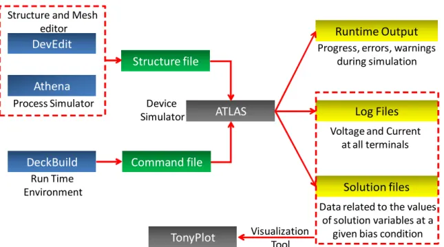
2.2. Silvaco framework overview
To simulate a structure via Silvaco, different tools are employed. In this work, we will focus on ATLAS that is a physically-based two and three dimensional device simulator that predicts the electrical behavior of semiconductor devices at specified bias conditions. The
Figure 2.1 Simulation flow in Silvaco showing the inputs and outputs of ATLAS DevEdit Athena Structure file Command file DeckBuild Runtime Output Log Files Solution files Process Simulator
Structure and Mesh editor Run Time Environment ATLAS Device Simulator
Progress, errors, warnings during simulation
Voltage and Current at all terminals
Data related to the values of solution variables at a
given bias condition
device structure containing the doping profiles and the mesh are inputted to ATLAS. One way to create the file is to start by the tool ATHENA to simulate the processing steps required to obtain the desired structure and then mesh it with a tool called DEVEDIT. Another way to create the structure file is by writing a script a DECKBUILD defining the mesh and the physical composition of the structure along with the doping profile.
The models, biasing conditions and numerical methods used to attain the electric characteristics are defined in ATLAS.
ATLAS will then generate three types of files: the runtime output which shows the progress of the simulation, the log files storing the current and voltage values at each electrode and finally the structure files containing information about various physical quantities inside the structure at certain biasing conditions. To visualize the output results, a tool called TONYPLOT is used to display the log and structures files. In this work, for better visualization, the results were extracted from TONYPLOT and plotted in Microsoft Excel. 2.3. Simulation of AlGaN/GaN HEMT
2.3.1. Meshing
In every conventional device simulator, to solve the physical equations governing the behavior of carrier transport, the device that is to be simulated is discretized into a grid and the equations are solved at each grip point. The grid and grip points are sometimes referred to as the mesh and nodes respectively. In our simulated structures, the mesh was generated in DECKBUILD. The most sensitive region in the HEMT transistor is the AlGaN/GaN interface. Therefore, as shown in figure 2.2, a very fine mesh was created in that region where the node-to-node distance in the y-direction was reduced down to 0.5 nanometers.
![Figure 1.5 Applications for various power devices along with the material capabilities [3]](https://thumb-eu.123doks.com/thumbv2/123doknet/2180988.10504/31.892.157.735.724.1013/figure-applications-various-power-devices-material-capabilities.webp)

![Figure 1.14 Comparison between different substrates on which GaN can be grown [3]](https://thumb-eu.123doks.com/thumbv2/123doknet/2180988.10504/39.892.218.670.113.400/figure-comparison-different-substrates-gan-grown.webp)
![Table 2.1 The values of the spontaneous polarization, lattice, elastic and strain constants for GaN and AlN [69][70][71]](https://thumb-eu.123doks.com/thumbv2/123doknet/2180988.10504/63.892.113.775.112.439/table-values-spontaneous-polarization-lattice-elastic-strain-constants.webp)