HAL Id: hal-03224199
https://hal.archives-ouvertes.fr/hal-03224199
Preprint submitted on 11 May 2021HAL is a multi-disciplinary open access
archive for the deposit and dissemination of sci-entific research documents, whether they are pub-lished or not. The documents may come from teaching and research institutions in France or abroad, or from public or private research centers.
L’archive ouverte pluridisciplinaire HAL, est destinée au dépôt et à la diffusion de documents scientifiques de niveau recherche, publiés ou non, émanant des établissements d’enseignement et de recherche français ou étrangers, des laboratoires publics ou privés.
Microscopic identification of the electric-field-driven
insulator to metal transition in a Mott insulator
D Babich, J Tranchant, C Adda, B Corraze, M.-P Besland, P Warnike, D
Bedau, P Bertoncini, J.-Y Mevellec, B Humbert, et al.
To cite this version:
D Babich, J Tranchant, C Adda, B Corraze, M.-P Besland, et al.. Microscopic identification of the electric-field-driven insulator to metal transition in a Mott insulator. 2021. �hal-03224199�
Microscopic identification of the electric-field-driven insulator to
metal transition in a Mott insulator
Authors: D. Babich1, J. Tranchant1, C. Adda1,5, B. Corraze1, M.-P. Besland1, P. Warnike4, D. Bedau2, P. Bertoncini1, J.-Y. Mevellec1, B. Humbert1, J. Rupp3, T. Hennen3, D. Wouters3,
R. Llopis5, L. Cario1,*,E. Janod1,*.
Affiliations:
1 Université de Nantes, CNRS, Institut des Matériaux Jean Rouxel, IMN, F-44000 Nantes,
France.
2 Western Digital Co, HGST, San Jose, CA 95135 USA.
3 Institut für Werkstoffe der Elektrotechnik II and Jülich-Aachen Research Alliance on
Fundamentals of Information Technology (JARA-FIT), RWTH Aachen University, D-52056 Aachen, Germany.
4 Paul Scherrer Inst, CH-5232 Villigen, Switzerland.
5 CIC nanoGUNE, Tolosa Hiribidea 76, 20018 Donostia-San Sebastian, Spain
*Correspondence to: Laurent.Cario@cnrs-imn.fr, etienne.janod@cnrs-imn.fr.
Abstract: Since the beginnings of the electronic age, a quest for ever faster and smaller switches has been initiated, since this element is ubiquitous and foundational in any electronic circuit to regulate the flow of current. Mott insulators are promising candidates to meet this need as they undergo extremely fast resistive switching under electric field. However the mechanism of this transition is still under debate. Our spatially-resolved µ-XRD imaging experiments carried out on the prototypal Mott insulator (V0.95Cr0.05)2O3 show that the resistive switching is associated with
the creation of a conducting filamentary path consisting in an isostructural compressed phase without any chemical nor symmetry change. This clearly evidences that the resistive switching mechanism is inherited from the bandwidth-controlled Mott transition. This discovery might hence ease the development of a new branch of electronics dubbed Mottronics.
Main Text: Much of the digital revolution that humanity is currently experiencing is due to the amazing development of a fundamental building block, the transistor. All key electronic components such as processors, volatile or non-volatile memories, running everyday objects like smartphones or computers are indeed based on the control of the conducting vs. insulator state of the transistor. However, the dimensional downscaling of this building block is now approaching fundamental limits giving an end to the Moore’s law and to traditional means of development of the microelectronics industry. As a result, new concepts for system architecture 1 and new materials for information processing and memory are being explored to extend the historical pace of progress observed over the last half-century. One of the proposed solutions is the Mottronics,
i.e. the use of Mott insulators in microelectronic devices2,3,4. These materials were among the most studied ones during the last decades owing to their outstanding electronic properties5,6. However, an insulator to metal transition (IMT) driven by a control parameter compatible with microelectronics, i.e. the electrical pulse, has only been demonstrated recently in Mott insulators. This property called Electric Mott Transition enabled the realization of breakthrough microelectronic devices, such as a Mott artificial neuron 7, a key building block for unconventional computation, or a new class of non-volatile memories and selectors2,8, and thus gives hope in the
realm of the Mottronics. But despite some significant advances9,10, some controversies exist concerning the nature of the metallic phase which persists after the application of the electric pulse and the exact role of the electronic correlation in the transition 11.
Here we study the electric Mott transition in the emblematic Mott insulator (V1-xCrx)2O3 and show
that the main recorded difference between the filamentary metallic phase and the insulating pristine material is a lattice contraction. Combining electronic transport, conducting-atomic force microscopy, Raman spectroscopy and µ-X-ray diffraction measurements, we bring out the strong analogy between the compressed phase within the filament and the metallic phase stable under pressure beyond the Mott insulator to metal transition12. The mechanism of the Electric Mott transition seems therefore deeply related to the physics of the Mott insulator to metal transition.
Modern band structure theories of Mott insulators predict the occurrence of two types of insulator to metal transitions (IMT), induced either through a change of the electronic filling or of the bandwidth, with practical near equilibrium implementations with charge doping and pressure application13,14. Studies dedicated to out-of-equilibrium IMT's in correlated systems are more recent. The first evidence of insulator to metal transitions induced by electric field in Mott insulators dates back to the early 2000s 15 and the same phenomenology was found afterwards in numerous other narrow gap Mott insulators, including the prototypal Mott insulator systems
(V1 - xCrx)2O3 16. In all these compounds, an electric field above a threshold value of a few kV/cm
is able to break the Mott insulating state and to induce a resistive switching. Several mechanisms have been proposed based on theoretical or experimental studies to explain the destabilization of the Mott state by electric field15,17,18, including Zener 11,19 or electronic avalanche effect 9,10. Numerous experimental and theoretical studies have also revealed that this resistive switching is related to the formation of a metastable filamentary conducting path 9,16,20,21. The stability in time of this filament depends on the electric pulse applied to the system. For pulses just above the threshold electric field, the filamentary path fully relaxes and disappears after the pulse, which leads to a volatile transition, while higher electric fields stabilize the filamentary path, inducing thus a non-volatile transition.
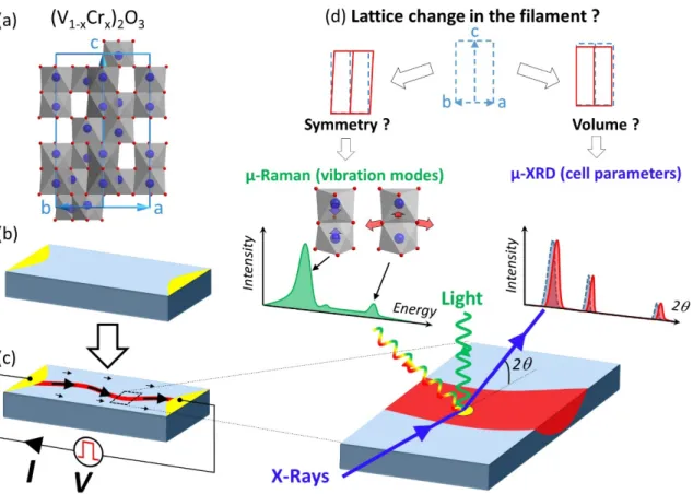
Figure 1 : overview of techniques used in this study to probe the electronic and structural consequences of the Electric Mott Transition (EMT) in Cr-doped V2O3. (a) View of the corundum structure of (V1-xCrx)2O3 in the
paramagnetic Mott insulator (PI) phase. (b-c) Schematic drawings of the samples (either a single crystal or a 150 nm thick thin film) patterned with electrodes (in yellow) before (b) and after (c) a non-volatile Electric Mott Transition. The path created after a non-volatile EMT, represented in red, is a conducting filament with modified electronic and structural properties. (d) In order to clarify the evolution (in particular a possible symmetry-breaking or a volume change) with respect to the pristine phase, the EMT-induced metallic filamentary phase was studied by μ-Raman and μ-X-Ray diffraction mapping.
Nevertheless, important questions remain unresolved. In particular, what is the nature of the metastable metallic phase induced by the Electric Mott Transition? Is the filamentary metallic phase qualitatively different from the one induced by the classical mechanisms, i.e. the bandwidth- and filling-controlled IMT’s ? Addressing these issues is of great fundamental interest as it could unravel an as yet unsolved basic property of highly correlated compounds placed out-of-equilibrium. But it could also facilitate the use of Electric Mott transitions in Mottronics devices thanks to a better control of this property. Figure 1 summarizes the approach used to clarify the nature of the electric-field-induced filamentary metallic phase. We studied the macroscopic electronic response, but also the concomitant lattice response of an emblematic Mott insulator, the chromium-doped vanadium sesquioxide (V1-xCrx)2O3. We mapped single crystals and patterned
thin films using two techniques spatially resolved at the micrometer scale and able to detect possible symmetry breakings and / or volume changes, namely Raman spectroscopy and X-ray diffraction.
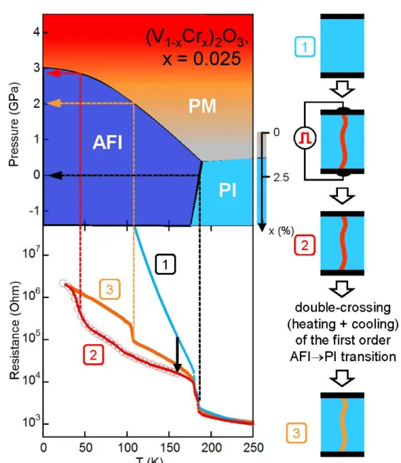
Figure 2 : (a) temperature – composition x – pressure phase diagram of (V1-xCrx)2O3. The pressure scale is
positioned for the composition x = 0.025, using the equivalence of 0.4 GPa per Cr percent proposed in Ref. 22. (b)
Electrical resistance vs temperature of a (V0.975Cr0.025)2O3 single crystal in its initial insulating state (1) and after
application of an electric pulse inducing the creation of a conducting filamentary path (2), as schematically represented in (c).
The rich phase diagram of the prototypal Mott insulator (V1-xCrx)2O3 reproduced in Figure 2-a was
established thanks to the pioneering work of McWhan et al. at Bell Labs fifty years ago 12.
Depending on chromium content (x), pressure (P) and temperature (T), three phases appear, the Paramagnetic (Mott) Insulator (PI), the Anti-Ferromagnetic (Mott) Insulator (AFI) and the Paramagnetic Metal (PM) phase. For a single crystal with chemical composition (V0.975Cr0.025)2O3,
a PI state is expected at room temperature, with a transition to an AFI state below 180 K. Figure 2- b presents the main results of our electronic transport study conducted on a (V0.975Cr0.025)2O3 single crystal. The resistance R vs. temperature T dependence in the pristine state
(curve #1) is in perfect agreement with the phase diagram (Figure 2-a), with a semiconducting-like behavior (dR/dT < 0) in the whole studied temperature range and a ten-fold increase of resistance at the transition temperature TPI → AFI = 180 K. This sample was then submitted to a 5µs
electric pulse (75 V ≡ 18 kV/cm / 5 µs) at 160 K, leading to a non-volatile Electric Mott Transition. The subsequent R(T) curve measured upon cooling (see curve #2 in Figure 2-b) reveals a substantial drop of electrical resistance and an unexpected feature at low temperature : a broad but well-defined increase of resistance around 40 K. The resistance drop may be easily explained by a simple model proposed for other Mott insulators 16,20 considering the creation of a conducting filament embedded in the pristine material and that percolates between the contact electrodes (see
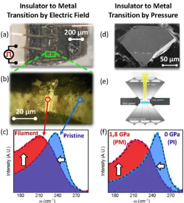
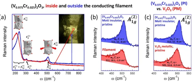
Figure 3 : comparison of Raman spectra of the metallic states obtained in (V1-xCrx)2O3 by application of an
electric field (left, x = 0.025) and of hydrostatic pressure (right, x = 0.038). (a) Image of the (V0.975Cr0.025)2O3
crystal, with four electrodes made of gold wires and carbon paste. Electric pulses were applied between neighboring electrodes, resulting in the creation of conducting filamentary paths. (b) Zoom on the region close to a filamentary path. (c) Raman spectra of the (V0.975Cr0.025)2O3 crystal obtained inside and outside the 4 µm
wide conducting filament shown in (b). (d) Scanning Electron Microscope image of the (V0.962Cr0.038)2O3 single
crystal used for Raman scattering experiments under pressure. (e) Schematics of the Diamond Anvil Cell used for Raman scattering under pressure. (f) Raman spectra of a (V0.962Cr0.038)2O3 crystal measured at room
temperature in the Diamond Anvil Cell close to ambient pressure in the Mott insulator states (PI) and at 1.8 GPa in the metallic state (PM, see Figure 2). Details about the fit of Raman spectra (dotted lines in (c) and (f)) are presented in Supplementary Materials.
Figure 2-c). In this model, the conductance of the filament becomes predominant at low temperature 12,23 and the additional resistance jump at 40 K in (V
1-xCrx)2O3 (see curve #2) hence
originates from a transition within the conductive filament. This gives some interesting clues about the nature of the metallic phase created after the electric pulse.According to the phase diagram shown in Figure 2-a, a resistivity jump at 40 K is indeed expected at the PM – AFI transition of (V0.975Cr0.025)2O3 put under a pressure of ≈ 3 GPa. This macroscopic transport study, presented
more in details in Supplementary Materials, suggests therefore that the electric pulse has created a filamentary path made of the same phase, but with a compressive strain strong enough to push it in the correlated metal phase (PM) at room temperature.
To confirm this lattice contraction, a direct visualization and study at the local scale of the crystallographic structure within the filament is required. A second crystal of composition (V0.975Cr0.025)2O3 issued from the same batch was hence subjected to a non-volatile Electric Mott
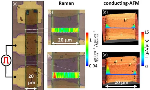
Figure 4 : Characterization of pristine and transited thin-film device by μ-Raman and conducting-AFM. (a) General image of 150 nm thick polycrystalline (V0.95Cr0.05)2O3thin film with a rectangular 170 x 20 μm shape
deposited on a SiO2/Si substrate patterned with TiN metallic electrodes. A schematic illustration of electrodes
connected to the electric pulse generator is shown. (b-c) Mapping of Raman intensities ratio measured at 210 and 230 cm-1 in the inter-electrode domains in the pristine (b) and transited (c) cases. (d - e) Conducting-AFM
mapping of the same regions shown in (b-c).
path bridging the two 25 µm apart conductive electrodes. The size of this filamentary structure allows to use Raman scattering to probe its crystallographic structure, thanks to the micrometric spatial resolution of this technique. The Raman spectra measured with a laser beam size of 1-2 µm both inside and outside the filament are shown in Figure 3–c and in Figure S-6 and S-7. Both spectra show only the usual signatures of the corundum structure of the (V1-xCrx)2O3 system 24,25,
i.e. a broad structure located between 180 and 280 cm-1 and two peaks around 300 and 500 cm- 1. No additional peaks are detected within the filament that could be associated either to a symmetry-breaking or to the formation of other VOx phases. However, the A1g Raman peak around 240-250
cm-1 measured in the filament is shifted by more than -20 cm-1 compared to the pristine Raman spectrum (see Figure 2-c). Moreover, a significant increase of the Raman signal is observed below 200 cm-1. These modifications of Raman spectra, discussed in more details in Supplementary Materials, support the existence of electronic and structural changes within the filament. To check if they could be assigned to a lattice contraction, a Raman study under pressure was then carried out at room temperature on a (V0.962Cr0.038)2O3 singlecrystal. For this composition, a
pressure-induced Mott insulator-to-metal transition is observed for a pressure above 1.2 GPa. The Raman spectra measured under 1.8 GPa at ambient pressure, displayed in Figure 3-f, disclose that this Mott transition causes both a shift of the A1g Raman vibration mode and an increase of Raman
intensity below 200 cm-1. Both changes are similar to the one observed between the pristine material and the core of the filamentary path created by the Electric Mott transition. Overall, this micro-Raman study provides additional evidences that the Electric Mott Transition yields a compressed, isostructural and metallic (V1-xCrx)2O3 filamentary phase. It strongly supports the
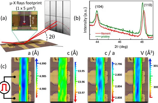
Figure 5 : μ-XRD mapping experiment on a (V0.95Cr0.05)2O3 thin-film device submitted to a Electric Mott
Transition. (a) Schematic view of the µ-XRD geometry, with a fixed incident angle of 11° between the X-Ray beam and the film, leading to an X-ray beam footprint of 1 μm wide and 5 μm long. A Dectris Eiger 4M 2D detector was used to register the Debye diffraction rings. The mapping was obtained by moving the sample holder with steps of 0.5 and 2.5 μm along two directions. (b) Comparison of µ-XRD diffractograms inside and outside the filamentary path. (c) Maps of lattice parameters a and c, as well as of the c / a ratio and the hexagonal unit cell volume extracted from XRD refinements of the 9191 measured diffractograms.
To further confirm the contraction of the lattice within the filament, a spatially resolved X-ray diffraction experiment was engaged using a 1 µm beam size at the micro-XAS beamline of the Swiss Light Source synchrotron facility. The penetration depth of X-ray being far bigger than the thickness of the filamentary path, we worked on polycrystalline thin films to maximize the signal coming from the filament over that of the matrix. In that purpose, a 150 nm polycrystalline
(V0.95Cr0.05)2O3 thin film with a rectangular 170 x 20 μm shape was deposited on a SiO2/Si
substrate patterned with TiN metallic electrodes (see Figure 4). Details about the preparation method of this device are given in Supplementary Materials. A 1 µs / 70 V electric pulse (≡ electric field E ≈ 35kV/cm) was applied at 160 K between two TiN electrodes to induce a non-volatile Electric Mott Transition. The sample was then characterized by conducting-atomic force microscopy (c-AFM) and by Raman spectroscopy. Atomic Force Microscopy (AFM) images shown in Figure 4-(d-e) reveal that the inter-electrode domain of the (V0.95Cr0.05)2O3film affected
by the Electric Mott Transition does not display any morphological change. Figure 4-(d-e) also shows the distribution of current measured by applying a 25 mV bias between the conductive AFM tip and the neighboring electrode, integrated over similar areas in regions affected by the EMT (Figure 4-e) and in pristine regions (Figure 4-d). Interestingly, the map shown in Figure 4-e unveils a clear ≈ 2 µm wide zone of higher conductivity close to the left edge of the (V0.95Cr0.05)2O3
stripe. Figure 4-c shows that the Raman mapping measured in the highly conducting region uncovered by c-AFM presents a tendency towards metallicity (ratio of Raman intensities between 210 and 230 cm-1 > 1, see Figure 3) compared to spectra measured outside of this zone. The c-AFM and Raman measurements confirm therefore the presence of a metallic filamentary path between the two inner electrodes of the polycrystalline device with features similar with those observed on the crystal.
A µ-XRD experiment was then engaged by mapping a 200 x 45 µm zone containing the whole patterned (V0.95Cr0.05)2O3 stripe of the device (170 x 20 µm). Details about the µ-XRD experiments are provided in Supplementary Materials. The map consists of 9191 (101 x 91) "pixels" of 5 x 1 µm, each of them corresponding to a 2D powder X-Ray diffractogram (see Figure 5-a). An azimuthal integration of the Debye rings was performed for each 2D powder X-Ray diffractogram to extract the intensity vs 2θ plots. Representative examples of the integrated diffraction patterns outside and inside the filament are shown in Figure 5-b. Outside the filament the diffraction pattern exhibits the expected Bragg peaks (104), (110) and (113) of the corundum structure. Inside the filament the same peaks are observed, but slightly shifted. Moreover, the absence of new diffraction peak discards the change of crystallographic symmetry or the formation of a chemical phase with different composition. The mechanism proposed in ref. 26, which suggests the creation of a V5O9 phase to explain the resistivity jumps in the low temperature phase, can therefore be excluded in our case. This crude comparison of XRD patterns in Figure 5-b already confirms that the (V0.95Cr0.05)2O3 phase within the filament keeps the corundum structure but with a different cell volume. The a and c unit cell parameters were then refined for each pixel based on the position of the (104), (110) and (113) Bragg peaks and were represented as maps in Figure 5-c. These maps reveal a remarkable feature : in the filamentary region bridging the two central electrodes, an increase of the c parameter (from 13.95 to 13.97 Å, ≈ + 0.15%) with respect to the rest of the sample is clearly observed. Conversely, the unit cell parameter a is contracted by about -0.4% compared to the normal zones. Overall the unit cell volume within this filament undergoes a contraction of -0.6% compared to the pristine material. This very specific behavior (c increase and a decrease) is strikingly similar with changes observed at the isostructural Mott transition driven by hydrostatic pressure12,27 shown in Figure S2. A + 0.26 % increase of c parameter and a - 0.65 % decrease of a parameter is indeed observed at the pressure induced Mott transition at room temperature for a (V0.972Cr0.028)2O3 single crystal 27. Conversely, our data do not point towards the
creation, within the filament, of a non-stoichiometric phase with a (V+Cr) : O ratio departing from 2:3. Indeed such non-stoichiometry induces a concomitant decrease of both a and c parameters28,29, which contrasts with the observed increase of the c parameter measured in the filamentary path shown in Figure 5-c.
The electronic transport and c-AFM measurements, as well as the μ-Raman and µ-XRD studies,
presented in this work are consistent with the creation by electric field of a metallic filamentary phase whose unit cell volume is contracted compared to that of pristine (V1-xCrx)2O3 Mott
insulator. Despite stimuli of seemingly very different nature, the electric-field-induced contraction resembles the one observed under pressure at the transition between the Mott insulator and paramagnetic metal. Interestingly, the pressure-induced volume contraction at the Mott transition can be rationalized within the compressible Hubbard model 30,31. In this approach, the lattice degrees of freedom react to the softening of electron degrees of freedom close to the Mott transition, resulting in a volume change of the lattice in order to avoid the unphysical situation of
negative bulk compressibilityi. The results presented in this paper strongly suggest that a similar
mechanism is at play at the Electric Mott transition, i.e. that the creation of excited and delocalized electrons during the electric pulses leads to a compressive lattice response. Overall, this work provides strong indication that Mott physics plays a pivotal role in the insulator to metal transition observed under electric field in (V1-xCrx)2O3. Our study therefore suggests that the relevant
theoretical approach to fully capture the Electric Mott Transition is the out-of-equilibrium compressible Hubbard model, which, to the best of our knowledge, has never been studied until now. Finally, the direct evidence of a lattice compression at the Electric Mott Transition in (V1 - xCrx)2O3 shown in this work rationalizes a posteriori the presence of electric-field-induced
superconductivity in the canonical Mott insulator GaTa4Se8 33,34, which is also superconducting
under pressure 35. This promotes the idea that the lattice compression at the Electric Mott Transition is a universal property of Mott insulators. Overall, the advances in understanding the mechanism of the Electric Mott Transition gained in this study will greatly facilitate the implementation of advanced Mottronics applications such as Resistive Mott memories and neuromorphic components in the near future 7,36.
References :
1. International Roadmap for Devices and Systems (IRDSTM) 2020 Edition - Beyond CMOS. (2020).
2. Tokura, Y., Kawasaki, M. & Nagaosa, N. Emergent functions of quantum materials. Nature
Physics 13, 1056–1068 (2017).
3. Zhou, Y. & Ramanathan, S. Mott Memory and Neuromorphic Devices. Proceedings of the
IEEE 103, 1289–1310 (2015).
4. Scheiderer, P. et al. Tailoring Materials for Mottronics: Excess Oxygen Doping of a Prototypical Mott Insulator. Advanced Materials 30, 1706708 (2018).
5. Bednorz, J. G. & Müller, K. A. Possible highT c superconductivity in the Ba−La−Cu−O system. Z. Physik B - Condensed Matter 64, 189–193 (1986).
6. Li, D. et al. Superconductivity in an infinite-layer nickelate. Nature 572, 624–627 (2019). 7. Stoliar, P. et al. A Leaky-Integrate-and-Fire Neuron Analog Realized with a Mott Insulator.
Advanced Functional Materials 27, 1604740 (2017).
8. Cario, L., Vaju, C., Corraze, B., Guiot, V. & Janod, E. Electric-Field-Induced Resistive Switching in a Family of Mott Insulators: Towards a New Class of RRAM Memories.
Advanced Materials 22, 5193–5197 (2010).
i A similar situation occurs at the first order liquid – gas phase transition, where the volume change at the transition
also occurs to avoid an unphysical negative bulk modulus. The equivalence between the Mott IMT and the liquid-gas transition is discussed in more details in ref. 32.
9. Guiot, V. et al. Avalanche breakdown in GaTa4Se8−xTex narrow-gap Mott insulators.
Nature Communications 4, 1722 (2013).
10. Diener, P. et al. How a dc Electric Field Drives Mott Insulators Out of Equilibrium. Phys.
Rev. Lett. 121, 016601 (2018).
11. Han, J. E., Li, J., Aron, C. & Kotliar, G. Nonequilibrium mean-field theory of resistive phase transitions. Phys. Rev. B 98, 035145 (2018).
12. McWhan, D. B. & Remeika, J. P. Metal-Insulator Transition in (V1-xCrx)2O3. Phys. Rev. B 2, 3734–3750 (1970).
13. Imada, M., Fujimori, A. & Tokura, Y. Metal-insulator transitions. Rev. Mod. Phys. 70, 1039– 1263 (1998).
14. Georges, A., Kotliar, G., Krauth, W. & Rozenberg, M. J. Dynamical mean-field theory of strongly correlated fermion systems and the limit of infinite dimensions. Rev. Mod. Phys. 68, 13–125 (1996).
15. Taguchi, Y., Matsumoto, T. & Tokura, Y. Dielectric breakdown of one-dimensional Mott insulators Sr2CuO3 and SrCuO2. Phys. Rev. B 62, 7015–7018 (2000).
16. Stoliar, P. et al. Universal Electric-Field-Driven Resistive Transition in Narrow-Gap Mott Insulators. Advanced Materials 25, 3222–3226 (2013).
17. Mazza, G., Amaricci, A., Capone, M. & Fabrizio, M. Field-Driven Mott Gap Collapse and Resistive Switch in Correlated Insulators. Phys. Rev. Lett. 117, 176401 (2016).
18. Li, J., Aron, C., Kotliar, G. & Han, J. E. Electric-Field-Driven Resistive Switching in the Dissipative Hubbard Model. Phys. Rev. Lett. 114, 226403 (2015).
19. Oka, T., Arita, R. & Aoki, H. Breakdown of a Mott Insulator: A Nonadiabatic Tunneling Mechanism. Phys. Rev. Lett. 91, 066406 (2003).
20. Vaju, C. et al. Electric-pulse-induced resistive switching and possible superconductivity in the Mott insulator GaTa4Se8. Microelectronic Engineering 85, 2430–2433 (2008).
21. Cario, L., Vaju, C., Corraze, B., Guiot, V. & Janod, E. Electric-Field-Induced Resistive Switching in a Family of Mott Insulators: Towards a New Class of RRAM Memories.
Advanced Materials 22, 5193–5197 (2010).
22. McWhan, D. B., Menth, A., Remeika, J. P., Brinkman, W. F. & Rice, T. M. Metal-Insulator Transitions in Pure and Doped V2O3. Phys. Rev. B 7, 1920–1931 (1973).
23. Lo Vecchio, I. et al. Optical properties of V2O3 in its whole phase diagram. Physical Review
B 91, (2015).
24. Kuroda, N. & Fan, H. Y. Raman scattering and phase transitions of V2O3. Phys. Rev. B 16, 5003–5008 (1977).
25. Tatsuyama, C. & Fan, H. Y. Raman scattering and phase transitions in V2O3 and (V1-xCrx)2O3. Physical Review B 21, 2977 (1980).
26. del Valle, J. et al. Electrically Induced Multiple Metal-Insulator Transitions in Oxide Nanodevices. Phys. Rev. Applied 8, 054041 (2017).
27. Rodolakis, F. Spectroscopies à l’aide du rayonnement synchrotron appliquées aux systèmes fortement corrélés: Transition métal-isolant dans les oxydes de vanadium. (Université Paris Sud - Paris XI, 2009).
28. Kuwamoto, H. & Honig, J. M. Electrical properties and structure of Cr-doped nonstoichiometric V2O3. Journal of Solid State Chemistry 32, 335–342 (1980).
29. Ueda, Y., Kosuge, K. & Kachi, S. Phase diagram and some physical properties of V2O3+x∗ (0 ⩽ x ⩽ 0.080). Journal of Solid State Chemistry 31, 171–188 (1980).
30. Majumdar, P. & Krishnamurthy, H. R. Lattice Contraction Driven Insulator-Metal Transition in the $d=\ensuremath{\infty}$ Local Approximation. Phys. Rev. Lett. 73, 1525–1528
(1994).
31. Hassan, S. R., Georges, A. & Krishnamurthy, H. R. Sound Velocity Anomaly at the Mott Transition: Application to Organic Conductors and V2O3. Phys. Rev. Lett. 94, 036402 (2005).
32. Georges, A., Florens, S. & Costi, T. A. The Mott transition: Unconventional transport, spectral weight transfers, and critical behaviour. J. Phys. IV France 114, 165–173 (2004). 33. Vaju, C. et al. Electric-Pulse-driven Electronic Phase Separation, Insulator–Metal Transition,
and Possible Superconductivity in a Mott Insulator. Advanced Materials 20, 2760–2765 (2008).
34. Ta Phuoc, V. et al. Optical Conductivity Measurements of GaTa4Se8 Under High Pressure: Evidence of a Bandwidth-Controlled Insulator-to-Metal Mott Transition. Phys. Rev. Lett. 110, 037401 (2013).
35. Abd-Elmeguid, M. M. et al. Transition from Mott Insulator to Superconductor in GaNb4Se8 and GaTa4Se8 under High Pressure. Physical Review Letters 93, (2004).
36. Adda, C. et al. Mott insulators: A large class of materials for Leaky Integrate and Fire (LIF) artificial neuron. Journal of Applied Physics 124, 152124 (2018).
Acknowledgments. Funding: The authors thank the University of Nantes for funding the PhD of D. B. in the framework of the French-Japanese International Associated Laboratory “Impacting Materials by Light and Electric pulses, and watching real-time Dynamics“ (IM-LED). The research leading to these results has received funding from the European 2020 research and innovation program under grant agreement n°730872 project CALIPSOplus. Author contributions: D. Babich : investigation, data curation, formal analysis, resources, validation ; J. Tranchant : conceptualization, investigation, writing – review & editing ; C. Adda : investigation, resources; B. Corraze : conceptualization, investigation, supervision, writing – review & editing ; M.-P. Besland : investigation, supervision ; P. Warnike: investigation, writing – review & editing ; D. Bedau : conceptualization, investigation, writing – review & editing ; P. Bertoncini : investigation, writing – review & editing ; J. - Y Mevellec : methodology, writing – review & editing ; B. Humbert : methodology ; J. Rupp : investigation, writing – review & editing ; T. Hennen : investigation, writing – review & editing ; D. Wouters : supervision ; R. Llopis : resources ; L. Cario : conceptualization, supervision, writing – original draft, writing – review & editing ; E. Janod : conceptualization, investigation, supervision, writing – original draft, writing – review & editing. Competing interests: Authors declare no competing interests. Data and materials availability: all data, code, and materials used in the analysis are available to any researcher for purposes of reproducing or extending the analysis.
Supplementary Materials: Materials and Methods Figures S1-S7
Supplementary Materials for
Microscopic identification of the electric-field-driven insulator to metal transition
in a Mott insulator
Correspondence to: Laurent.Cario@cnrs-imn.fr, etienne.janod@cnrs-imn.fr
This PDF file includes:
Materials and Methods Supplementary Text Figs. S1 to S7
Materials and Methods
Details on experimental techniques
1. Transport and electric pulse application
The low-bias resistance was measured using either a Keithley 236 source-measure unit or a Keithley 6221 current source associated with a Keithley 2182A nanovoltmeter. For the electric pulses application, thin-film devices and crystals were connected in series with a load resistance
Rload playing the role of the current limiter and ranging in the 5–10% of the sample resistance.
Voltage pulses were applied using either a pulse generator Agilent 8114 or an arbitrary function generator Agilent 81150A.
2. Conducting Atomic Force Microscopy
Conductive – AFM measurements were performed in air using the c-AFM module of the Multimode 8 nanoscope V (Bruker). Conducting platinum silicide coating tips were used (SCM-PTSI, Bruker).
3. Raman spectroscopy
Raman spectra were recorded using a microRaman Invia (Renishaw) using an excitation at 785 nm. The spectral resolution achieved with the use of gratings of 1200 grooves per millimeter was 3 cm-1. The microscope was equipped with an automated XYZ table allowing mapping with a spatial resolution of 1µm.
Raman scattering experiments under pressure were performed in the Membrane Diamond Anvil Cell (MDAC) schematized in
Figure S 1-a. The (V0.962Cr0.038)2O3 single crystal and a few ruby micro-crystals were
placed in the pressure chamber prepared by drilling a 300 µm hole in a stainless steel gasket (see Figure S 1-b-c). Pure methanol was used as pressure transmitting medium. The pressure was estimated by monitoring the fluorescence lines of ruby excited by a 514 nm laser. Two Raman spectra, measured on the (V0.962Cr0.038)2O3 crystal using a 785 nm laser, are shown in
Figure S 1-d. The broad contribution between 350 and 700 cm -1 corresponds to the Raman signal of methanol, and complicates the measurement and interpretation of the 𝐴𝐴1𝑔𝑔(2) phonon of (V0.962Cr0.038)2O3 around 510 cm-1.
Figure S 1 : (a) schematic drawing of the Diamond Anvil Cell (DAC) used for Raman under pressure experiments. (b) Image of the gasket drilled with a 300 µm hole to define a pressure chamber, taken from the top of the DAC. (c) Optical image of the single (V0.962Cr0.038)2O3 crystal
inside of the pressure chamber. Inset : Scanning Electron Microscope Image of the crystal. (d) Typical Raman spectra of (V0.962Cr0.038)2O3 measured inside of the DAC, at room pressure in the
PI state and at 1.8 GPa in the PM state.
4. Micro-X-Rays Diffraction mapping experiments
µ-X-ray diffraction experiments were carried out at the µ-XAS beamline (SLS Synchrotron, Switzerland). We chose a rather low X-Rays energy of 6.1 keV (λ = 2.0325 Å) in order to keep a beam diameter as small as 1µm. The calibration of the experiment geometry (sample-detector distance, orientation of the Dectris Eiger 4M two-dimensional detector with respect to the beam) was performed with the standard compound Na2Ca3Al2F14. An XRD experiment was performed
using powders of this material inserted into a glass capillary placed at the same position as the sample. The calibration procedure was done using the Fast Azimuthal Integration pyFAI python package1.
In order to map the 170 x 20 µm stripe of (V0.95Cr0.05)2O3 thin film shown in Figure S 4.a,
9191 two-dimensional images were recorded during the µ-XRD experiment (4 seconds per (x,y) position total measurement time ≈ 10 h). We moved the sample holder with 0.5 µm steps along (101 steps) and perpendicular (91 steps) to the (V0.95Cr0.05)2O3 stripe direction, resulting in a total
map size of 250 x 45 µm. Each of the 9191 diffractograms was then azimuthally integrated to obtain a 1D “Intensity versus Q” curve. Then the position of the (104), (110) and (113) Bragg peaks were fitted on each diffractogram to extract the a and c unit cell parameters shown in Figure 5 of the article.
We note that the thin film preparation process described in the next section led to an edge effect. As shown in Figure 5 of the article, all the edges of the (V0.95Cr0.05)2O3 stripe indeed display
a slightly compressed unit cells a parameter and volume compared to the center of the stripe. This effect explains the increased electrical conductivity close to the edges, which appears even in the pristine state as indicated by Figure 4.d of the article. These edges with a slightly enhanced conductivity in the pristine state explains why the filamentary path was created close to an edge during the electric Mott Transition, as indicated in Figures 4 and 5 of the article. However, the evolution of the c parameter shown in Figure 5.c clearly proves that there is a qualitative difference between the overall volume contraction induced by the Electric Mott Transition and that observed at the edges in the pristine state. Almost no edge effect is indeed detected for the c unit cell parameter in the pristine state, while a clear increase of c appears in the filamentary path created during the EMT. This clearly demonstrate that the compressive edge effect in the pristine state is
Figure S 2 : (a-b) Evolution with pressure of the unit cell parameters c and a of a (V0.972Cr0.028)2O3
powder, extracted from ref. 2. (c) Deduced variation of the unit cell volume with pressure.
too small to generate a full insulator to metal transition. Conversely, both fingerprints of the insulator to metal transition, namely a drop of the a parameter and an increase of c, appears inside of the filamentary path created during the Electric Mott Transition.
Samples and device preparation
1. (V1-xCrx)2O3 single crystals : synthesis and characterization
The (V1-xCrx)2O3 single crystals used for transport and Raman measurements were prepared
using a sulfur-assisted chemical-vapour transport method. The synthesis is performed in two steps. After a first drying at 400°C, V2O5 powder (Aldrich, >99.6%) was mixed with Cr2O3 (Prolabo,
99.9%) in the appropriate ratio. The mixture was then placed in an oven at 900°C for 10 h under a 95% Ar–5% H2 gas flow. Half a gram of the pure (V1-xCrx)2O3 obtained powder was then
introduced in a silica tube, with 40 mg of sulfur as a vapor phase transport agent. The tube was vacuum sealed, heated up to Tmax (950-1050°C) in a furnace with a temperature gradient (≈
10°C/cm), slowly cooled down to 900°C (from - 0.5 to - 2°C/h) and finally fast cooled (−300°C/h) to room temperature. Such treatment allows obtaining small single crystals (typical size <300 μm) within the preparation. The chromium substitution rate on each individual crystal used in this work was determined by Energy-dispersive X-ray spectroscopy (EDXS) analyses carried out using a scanning electron microscope JEOL 5800.
2. Device based on (V0.95Cr0.05)2O3 thin film
The patterned planar devices used in this work (see Figures 4 and 5 of the main text) were fabricated within a collaboration between the Jean Rouxel Institute of Materials (France) and the CIC nanoGUNE (Spain). The main steps of the fabrication process, depicted in Figure S 3, consist
(c) (a) (b) ∆c/c = + 0.26 % ∆a/a = - 0.65 % 293 295 297 299 0 0.5 1 1.5 2 2.5 (V0.972Cr0.028)2O3 V o lum e ( Å 3 ) P (GPa)
(∆V/V)
transition=
- 1.04 %
in :
- step 1 : deposition of TiN (electrode material),
- step 2 : photolithography to design the electrode pattern and etching of TiN, - step 3 : photolithography to design the active material pattern,
- step 4 : deposition, lift-off and annealing of active material (V0.95Cr0.05)2O3 thin film
The 150 nm thick (V0.95Cr0.05)2O3 films were deposited by a co-sputtering technique at room
temperature, and were then annealed under a controlled reducing atmosphere at 500° C for 10 h. Details about the synthesis conditions are given in ref. 3. Chemical analyses performed by EDXS confirm the presence of three elements V, Cr, and O in the films and give a Cr/(V + Cr) ratio of 0.053(4) in good agreement with the targeted chemical composition.
After the application of the electric pulses leading to the resistive switching, the samples used in this study (see Figure 4 and 5 in the article) were characterized by Scanning Electron Microscopy (SEM) and conducting - Atomic Force Microscopy (c-AFM). It clearly appears both in Figure S 4-a-b (SEM) and Figure S 4-c (c-AFM) that the resistive switching does not result in any visible microstructural changes compared to a pristine state.
Figure S 3 : Fabrication process of the patterned planar devices made of titanium nitride electrodes and (V1.95Cr0.05)2O3 thin film as active material.
Figure S 4 : Scanning Electron Microscope (a-b) and Atomic Force Microscope (AFM) images (c) of a device based on (V0.95Cr0.05)2O3 thin film. The images were obtained after the application
of electric pulses yielding the Electric Mott Transition (see Figures 3-4 in the main article). The z-profile of the 170 µm long / 20 µm wide polycrystalline (V0.95Cr0.05)2O3 stripe is represented in
the lower part of (c), and indicates a film thickness of 150 nm. AFM images were analyzed using the WSxM software package4.
3. Electrodes contacting on (V1-xCrx)2O3 single crystals and thin film devices
Electrical characterizations were performed on several (V1-xCrx)2O3 crystals and on devices
based on (V1.95Cr0.05)2O3 thin film contacted with 17 μm gold wires using a carbon paste
(Electrodag PR-406) and then annealed in vacuum at 150°C for 30 min to achieve a low contact resistance.
Supplementary Text
Transport study on the (V0.975Cr0.025)2O3 single crystal
Figure 2 of the article discloses a part of a broader transport study carried out on a (V0.975Cr0.025)2O3 single crystal before and after an Electric Mott Transition. The results of an
extended study is depicted in Figure S 5. After measuring the resistance vs temperature curve in the pristine insulating state and just after the application of electric pulses, the (V0.975Cr0.025)2O3
was then submitted to several cooling - warming cycles between 40 and 300K. In the first temperature cycle, a resistance jump appears around 40 K (red open circles, curve #2 in Figure 2 and in Figure S 5). Upon heating (red filled circles, curve #2 in Figure S 5), the jump in the R(T) curve around 40 K is essentially unmodified, with only a small hysteresis of ≈ 1K. At higher temperature, an attenuated R(T) drop persists at the AFI → PI transition, and the resistance almost superimposes that of the pristine compound above 180 K. Surprisingly, after less than fifteen minutes spent at 290 K, the R(T) curve measured subsequently by cooling again from room to low temperature (see curve #3 in Figure S 5) unveils a huge shift of the low temperature transition from 40 K to 105 K. Subsequent “warming to 290 K – cooling down to 40 K” cycles did no longer modify the resistance curve, with a low temperature transition maintained at 105 ± 2 K.
As mentioned in the article, these observations can be explained by the creation of a conducting filament which percolates between the contact electrodes. This explanation was already proposed for other Mott insulators,5 but it has a striking consequence in (V
1-xCrx)2O3.
Above the transition temperature TPI→AFI, the conductance of the filament is indeed low compared
to that of the pristine part, letting the macroscopic resistivity almost unchanged. Conversely, the conductance of the filament becomes predominant below TPI → AFI = 180K, since the conductance
of the pristine part (curve #1 in Figure S 5) decreases sharply in the AFI phase.6,7 As a consequence the additional resistivity jumps observed at 40 K in curves #2 and then at 105 K in curve #3 are attributed to transitions within the conductive filament. These transitions give therefore some clues about the nature of the metallic phase created after the electric pulse. According to the phase diagram of the (V1 - xCrx)2O3 system, the resistivity jumps observed at 40 K and 105 K could
correspond to the PM – AFI transitions that exist at these temperatures in (V0.975Cr0.025)2O3 put
under pressure at ≈ 3 GPa and ≈ 2 GPa, respectively. Therefore, these measurements strongly suggest that the electric pulse has created a filamentary path made of the same phase, but under a compressive strain corresponding to a pressure of 2 - 3 GPa, i.e. strong enough to make it metallic. Within this picture, the shift of the transition temperature from 40 K to 105 K is simply explained by the strain relaxation caused by the double crossing (i.e. by heating and then cooling) of the AFI → PI transition in the pristine zone surrounding the filament. The abrupt changes of the a (+0.24 %) and c (-0.57 %) parameters of the pristine zone at the transition6 might indeed relax the stress state of the filament and explain the transport properties shown in Figure S 5. Finally, the shift of the transition temperature observed after bringing back the sample to room temperature discards a possible change of stoichiometry within the filamentary path. At this temperature the ionic mobility is indeed far too low to induce a stoichiometry change in a measurable time.
Figure S 5 : Results of extended transport study on a (V0.975Cr0.025)2O3 single crystal submitted
to Electric Mott Transition at 160 K, in complement to Figure 2 in the article.
Complementary Raman spectroscopy data on (V1-xCrx)2O3 single crystals
In complement with the Raman study of the conducting filament shown in Figure 3 of the article, we present here additional Raman data obtained on the same (V0.975Cr0.025)2O3 crystal in
the PI phase and in the PM phase under pressure, as well as on a Cr-free V2O3 crystal in the PM
phase. Both crystals crystallize in the 𝑅𝑅3�𝑐𝑐 corundum crystallographic structure with the D3d point
group8. Seven Raman-active modes are expected, two A1g and five Eg modes. Figure S 6 shows
that three intense Raman modes can be clearly identified in (V1-xCrx)2O3 (x = 0.025), which can
Figure S 6 : (a) Full Raman spectra measured inside (red curve) the conducting filament and outside in the pristine state (blue curve). The atomic displacements associated with the three most intense Raman modes are schematically represented.9 (b) Same Raman spectra as in (a), zoomed on the 𝐴𝐴1𝑔𝑔(2) mode (see text). (c) Comparison of the 𝐴𝐴1𝑔𝑔(2) mode measured in the PI phase on a (V0.975Cr0.025)2O3 crystal and in the PM phase on a V2O3 crystal at room temperature. The strongly
asymmetric shape results from a Fano resonance, i.e. a coupling between the 𝐴𝐴1𝑔𝑔(2) phonons and electronic transitions within the a1g – bonding band10. Accordingly, the Raman modes were fitted
according to a model appropriate to describe the Fano effect : 𝐼𝐼(𝜔𝜔) = 𝐼𝐼0(𝑞𝑞 + 𝜀𝜀)2/(1 + 𝜀𝜀²), with 𝜀𝜀 = (𝜔𝜔 − 𝜔𝜔0)/𝛤𝛤, where ω0 is the resonance frequency, Γ is a measure of the line width, and q-1 is
the Fano coupling coefficient. Clearly, q-1 is enhanced (or equivalently q is lowered) in the metallic phases with respect to the PI value, both in the standard PM phase of pure V2O3 and in the
conducting filament.
In the article, Figure 2-c shows the changes in Raman spectra between the pristine state and the metallic state in the conducting filament in the energy window 170-290 cm-1. Figure S 6-a shows the same data on a larger energy window (170 - 850 cm-1). This global view shows that essentially the same Raman vibration modes appear inside and outside of the conducting filament: two A1g modes around 240 cm-1 (𝐴𝐴1𝑔𝑔(1)) and 510 cm-1 (𝐴𝐴1𝑔𝑔(2)), as well as an Eg modes of weak
intensity around 210 cm-1 (𝐸𝐸
𝑔𝑔(1)) and another more intense one at 305 cm-1 (𝐸𝐸𝑔𝑔(2)). These
measurements, in perfect agreement with the studies published in the system (V1 - xCrx)2O311,12
support the scenario of a filament made up exclusively of the phase (V1 - xCrx)2O3 phase, without
any other phase of different chemical composition.
In the article, Figure 3 shows that a softening of the 𝐴𝐴1𝑔𝑔(1) mode occurs in the filament, very similar to that appearing at the pressure – induced insulator transition. Figure S 6-b shows that the 𝐴𝐴1𝑔𝑔(2) mode around 510 cm-1 presents a similar shift, but also a striking change in the peak shape of the filament compared to the pristine state. The 𝐴𝐴1𝑔𝑔(2) peak in the filament indeed becomes broader and becomes more asymmetric with an increasing weight on the low energy side. Interestingly, Figure S 6-c shows that these three characteristic evolutions of the 𝐴𝐴1𝑔𝑔(2)mode, namely softening,
broadening and increasing asymmetry, are also observed at the composition-induced insulating (PI) to metal (PM) transition between (V0.975Cr0.025)2O3 and V2O3. On the theoretical side, the
anomalous asymmetric line shape has been assigned to a Fano resonance effect between the A1g
phonons and electronic transitions within the a1g – bonding band.10 According to this approach,
the smaller asymmetry observed in the insulating phases results from a lower population of the a1g
electronic band.13
Interestingly, the study carried out in ref. 10 has demonstrated that the asymmetry effect is also very strong for the 𝐴𝐴1𝑔𝑔(1) phonon located around 240 cm-1. Figure S 7-a-b shows that the Raman spectrum between 160 and 290 cm-1 can be decomposed as the sum of two phonons modes, a
symmetrical 𝐸𝐸𝑔𝑔(1) mode and an asymmetrical 𝐴𝐴1𝑔𝑔(1) mode.
The same decomposition is also able to describe the Raman spectra on both sides of the pressure-induced insulator to metal transition, as shown in Figure S 7-d. The comparison between the electric–field-induced and pressure-induced transitions clearly shows a similar evolution of the asymmetry and linewidth parameters. The only difference between these two samples is the frequency of the 𝐴𝐴1𝑔𝑔(1) phonon mode, 253 cm-1 in the crystal used for pressure experiments against
245 cm-1 for the one used under electric field. Figure S 7-e shows that this small difference results
from slightly different composition of these two crystals, xCr = 3.8 % and 2.5 %, respectively.
Overall, these analyses of Raman spectroscopy in (V1-xCrx)2O3 single crystals demonstrate
that the electric-pulse-induced conducting filament (i) is composed only of (V1-xCrx)2O3, without
any other phase with different chemical composition, and (ii) presents vibrational signature similar with those observed at the pressure- and composition-induced insulator to metal transitions.
Figure S 7 : (a-b) same Raman data as in Figure S 6, but zoomed on the low energy part of the spectra.
References Supplementary Informations
1. Ashiotis, G. et al. The fast azimuthal integration Python library: pyFAI. J Appl Crystallogr 48, 510–519 (2015).
2. Rodolakis, F. Spectroscopies à l’aide du rayonnement synchrotron appliquées aux systèmes fortement corrélés: Transition métal-isolant dans les oxydes de vanadium. (Université Paris Sud - Paris XI, 2009).
3. Querré, M. et al. Metal–insulator transitions in (V1-xCrx)2O3 thin films deposited by
reactive direct current magnetron co-sputtering. Thin Solid Films 617, Part B, 56–62 (2016). 4. Horcas, I. et al. WSXM: A software for scanning probe microscopy and a tool for
nanotechnology. Review of Scientific Instruments 78, 013705 (2007).
5. Vaju, C. et al. Electric-pulse-induced resistive switching and possible superconductivity in the Mott insulator GaTa4Se8. Microelectronic Engineering 85, 2430–2433 (2008).
6. McWhan, D. B. & Remeika, J. P. Metal-Insulator Transition in (V1-xCrx)2O3. Phys. Rev. B 2, 3734–3750 (1970).
7. McWhan, D. B., Menth, A., Remeika, J. P., Brinkman, W. F. & Rice, T. M. Metal-Insulator Transitions in Pure and Doped V2O3. Phys. Rev. B 7, 1920–1931 (1973).
8. Dernier, P. D. The crystal structure of V2O3 and (V0.962Cr0.0382)2O3 near the metal-insulator transition. Journal of Physics and Chemistry of Solids 31, 2569–2575 (1970). 9. Yang, H. & Sladek, R. J. Lattice-dynamical model for the elastic constants and Raman
frequencies in (V1-xCrx)2O3. Physical Review B 32, 6634 (1985).
10. Okamoto, A., Fujita, Y. & Tatsuyama, C. Raman Study on the High Temperature Transition in V2O3. Journal of the Physical Society of Japan 52, 312–317 (1983).
11. Kuroda, N. & Fan, H. Y. Raman scattering and phase transitions of V2O3. Phys. Rev. B 16, 5003–5008 (1977).
12. Tatsuyama, C. & Fan, H. Y. Raman scattering and phase transitions in V2O3 and (V1-xCrx)2O3. Physical Review B 21, 2977 (1980).
13. Park, J.-H. et al. Spin and orbital occupation and phase transitions in V2O3. Phys. Rev. B 61, 11506–11509 (2000).