HAL Id: tel-00194584
https://tel.archives-ouvertes.fr/tel-00194584
Submitted on 6 Dec 2007HAL is a multi-disciplinary open access
archive for the deposit and dissemination of sci-entific research documents, whether they are pub-lished or not. The documents may come from teaching and research institutions in France or abroad, or from public or private research centers.
L’archive ouverte pluridisciplinaire HAL, est destinée au dépôt et à la diffusion de documents scientifiques de niveau recherche, publiés ou non, émanant des établissements d’enseignement et de recherche français ou étrangers, des laboratoires publics ou privés.
To cite this version:
Olivier Ginez. Fault Modeling and Testing of Flash Memories. Micro and nanotechnolo-gies/Microelectronics. Université Montpellier II - Sciences et Techniques du Languedoc, 2007. English. �tel-00194584�
T H E S E pour obtenir le grade de
DOCTEUR DE L'UNIVERSITE MONTPELLIER II
Spécialité : Microélectronique.
Formation Doctorale : Systèmes Automatiques et Microélectroniques. Ecole Doctorale : Information, Structures et Systèmes.
présentée et soutenue publiquement
par
Olivier GINEZ
le 29 Novembre 2007
Modélisation de Fautes et Test des Mémoires Flash
(
Fault Modeling and Testing of Flash Memories)JURY
M. Dominique Dallet, Professeur, IMS, ENSEIRB, Bordeaux Rapporteur M. Jean-Michel Portal, Maître de Conférences, L2MP, Polytech’ Marseille Rapporteur
M. Jean-Michel Daga, Sté ATMEL, Rousset Examinateur
M. Arnaud Virazel, Maître de Conférences, Université Montpellier II – LIRMM Examinateur M. Joan Figueras, Professeur, Politecnica de Catalunya, Barcelone Membre Invité M. Patrick Girard, Directeur de Recherche CNRS, LIRMM Directeur de Thèse M. Serge Pravossoudovitch, Professeur, Université Montpellier II – LIRMM Co-Directeur de Thèse
A ma fille et à ma femme dont le soutien et la présence m’ont permis de mener cette thèse à bien.
A mon grand-père qui je l’espère est fier de moi même si parfois le chemin que je trace n’est pas toujours droit.
Remerciements
Cette thèse a été effectuée au Laboratoire d’Informatique de Robotique et de Microélectronique de Montpellier (LIRMM), dirigé par Monsieur Michel Robert, Professeur à l’Université de Montpellier II, dans le département Microélectronique dont le responsable est Monsieur Lionel Torres, Professeur à l’Université de Montpellier II. Je les remercie de m’avoir accueilli.
Toute ma gratitude va à mon directeur de thèse, Patrick Girard, Directeur de Recherche au CNRS, dont l’encadrement très professionnel, la présence et les encouragements constants m’ont permis d’évoluer en thèse en toute sérénité. Je voudrais qu’il trouve ici toute l’expression de ma reconnaissance.
Je tiens à remercier mon co-directeur de thèse Serge Pravossoudovitch, Professeur à l’Université de Montpellier II, dont la pédagogie a suscité en moi l’envie d’enseigner mais aussi d’avoir bien voulu présider le jury chargé de juger ma thèse.
Je remercie aussi Christian Landrault ainsi qu’Arnaud Virazel pour m’avoir encadrer avec beaucoup d’enthousiasme durant ces trois années mais aussi pour m’avoir tant apporté sur le plan scientifique et technique. La thèse nous prouve parfois qu’il ne s’agit pas forcément que d’une histoire de scientifiques mais aussi d’hommes !
Je voudrais également remercier Jean-Michel Daga, Manager de l’équipe conception de mémoires non-volatiles dans la société ATMEL, qui m’a beaucoup aidé tout au long de cette thèse tant sur l’aspect technique qu’industriel de mes travaux. Sa vision pragmatique et son esprit de synthèse ont été très précieux pour mener à bien cette thèse. Je lui adresse ici mes remerciements les plus sincères.
Je remercie également Messieurs Dominique Dallet, Professeur à l’ENSEIRB de Bordeaux, Joans Figueras, Professeur à l’Université de Catalogne, et Jean-Michel Portal, Maître de Conférences à Polytech’ Marseille, de s’être intéressés à ce travail de thèse et d’avoir accepté d’en être les rapporteurs. Qu’ils trouvent ici toute l’expression de ma reconnaissance.
Enfin, je terminerais en remerciant tous mes collègues du laboratoire pour les bons moments que nous avons passés ensemble, Grand Nico, Petit Nico, Marie, Lio, Alex N, Alex R, Fab, Alin, Seb, Robin, Olivier B, Nico H, JE, Julien V, Julien D, Olivier L, Marion, Mehdi, Olivier H, Luigi, Norbert, Réou, JB, JD, Diego.
Index
INDEX --- 4
GENERAL INTRODUCTION --- 6
CHAPTER 1: IN THE FIELD OF NON-VOLATILE MEMORIES --- 10
1.1 SEMICONDUCTOR MEMORIES: STATE OF THE ART --- 10
1.1.1 VOLATILE MEMORIES--- 11 1.1.1.1 Sram--- 11 1.1.1.2 Dram --- 11 1.1.2 NON-VOLATILE MEMORIES--- 12 1.1.2.1 Rom--- 12 1.1.2.2 Eprom --- 13 1.1.2.3 Eeprom--- 13 1.1.2.4 Flash --- 14
1.1.3 FUTURE NON-VOLATILE MEMORIES--- 15
1.1.3.1 Phase Change Memories --- 15
1.1.3.2 FeRam --- 16
1.2 NON-VOLATILE MEMORY TECHNOLOGY --- 17
1.2.1 FLOATING GATE TECHNOLOGY--- 17
1.2.2 CHARGE TRAP TECHNOLOGY--- 19
1.2.2.1 Mnos Technology--- 19
1.2.2.2 Sonos Technology --- 20
1.3 EMBEDDED FLASH (EFLASH) MEMORIES BUILT WITH FLOTOX CORE CELLS--- 21
1.3.1 EFLASH MEMORIES ARCHITECTURE--- 21
1.3.2 EFLASH MEMORY FUNCTIONING--- 23
1.4 CONCLUSION --- 24
CHAPTER 2: GENERAL ASPECTS ON MEMORY FAULT MODELING AND TESTING --- 26
2.1 BACKGROUND OF RAM FAULT MODELING AND TESTING --- 26
2.1.1 RAM FAULT MODELS--- 27
2.1.2 RAM TEST ALGORITHMS--- 29
2.2 BACKGROUND OF FLASH MEMORY FAULT MODELING AND TESTING --- 32
2.2.1 THE 7-PATTERNS TEST SEQUENCE--- 32
2.2.2 THE 5-STEPS TEST SEQUENCE--- 34
2.2.3 AN EFLASH FAULT SIMULATOR TO EVALUATE A BASIC TEST FLOW--- 36
2.3 MARCH ALGORITHMS APPLIED TO EFLASH MEMORY --- 37
2.3.1 EFLASH COMPARED TO RAM--- 37
2.3.2 EVALUATION OF MARCH ALGORITHMS IN EFLASH--- 38
2.4 CONCLUSION --- 40
CHAPTER 3: ANALYSIS AND MODELING OF ACTUAL EFLASH DEFECTS AND RELATED FAILURE MECHANISMS --- 41
3.1 QUALITATIVE ANALYSIS OF FAILURE MECHANISMS IN FLOTOX CORE CELLS EFLASH-- 41
3.1.1 EXPERIMENTAL SET-UP AND FAILURE CLASSIFICATION--- 41
3.1.2 HARD DEFECT RELATED FAILURES--- 43
3.1.3 RESISTIVE DEFECT RELATED FAILURES--- 44
3.1.4 FLOATING GATE TRANSISTOR RELATED FAILURES--- 47
3.1.5 DISTURB PHENOMENON--- 48
3.2 A SPICE-LIKE FLOTOX ELECTRICAL MODEL FOR FAULTY BEHAVIOR PREDICTION --- 51
3.2.1 DESCRIPTION OF THE SIMULATION MODEL--- 52
3.2.3 FURTHER IMPROVEMENTS OF THE MODEL--- 58
3.3 RESISTIVE DEFECT INJECTION IN THE FLOTOX CORE CELL ARRAY --- 58
3.3.1 DEFECT INJECTION SET-UP--- 59
3.3.2 RESISTIVE SHORT BETWEEN METAL AND POLY-SILICON LAYERS--- 61
3.3.3 RESISTIVE SHORT BETWEEN TWO POLY-SILICON LAYERS--- 69
3.4 SUMMARY AND DISCUSSION ON TEST SOLUTIONS --- 74
CHAPTER 4: TESTING OXIDE THICKNESS VARIATION OF THE TUNNEL WINDOW --- 75
4.1 ORIGIN OF THE COUPLING PHENOMENON --- 75
4.1.1 INFLUENCE OF THE DISTURB VOLTAGE--- 77
4.1.2 FAULT MODELING OF THE OXIDE THICKNESS VARIATION OF THE TUNNEL WINDOW--- 78
4.2 TESTING SOLUTION FOR AN OXIDE THICKNESS VARIATION--- 79
4.2.1 SENSITIZATION SEQUENCE--- 79
4.2.2 PARALLEL PROGRAMMING APPROACH--- 82
4.3 CONCLUSION --- 83
CHAPTER 5: TESTING FOR ADDRESS DECODER FAULTS IN EFLASH MEMORIES--- 85
5.1 INTRODUCTION TO ADDRESS DECODER FAULTS (AFS) IN EFLASH --- 85
5.1.1 EFLASH DECODING CIRCUITRY--- 85
5.1.2 TYPES OF AFS IN AN EFLASH--- 87
5.1.3 BASIC OPERATIONS FOR AFS DETECTION--- 88
5.1.4 SIMILARITIES BETWEEN AFS IN EFLASH AND RAM --- 91
5.2 CONCURRENT APPROACH FOR TESTING ADDRESS DECODER FAULTS --- 92
5.2.1 AFS TESTING IN THE WLIDECODER--- 92
5.2.2 AFS TESTING IN THE BLJDECODER--- 97
5.2.3 AFS TESTING SUMMARY--- 98
5.3 OPTIMIZATION OF THE AFS TESTING STRATEGY--- 99
5.3.1 AFS TESTING TIME EVALUATION---100
5.4 CONCLUSION --- 101 GENERAL CONCLUSION --- 103 SCIENTIFIC CONTRIBUTIONS --- 106 REFERENCES --- 108 LIST OF FIGURES --- 112 LIST OF TABLES --- 113
General Introduction
Since the transistor invention, a lot of microelectronics components have been developed in academic laboratories or in semi-conductor companies. One of the most used microelectronic components is the memory circuit. The memory business has started to increase at the beginning of the 70’s with the arrival of the first microprocessor (4004) developed in 1968 by Intel. Nowadays, semi-conductor memories are not only used in microprocessors but also in each electronic device developed for information or communication application fields. The memory market has continued to increase drastically in the last years and now achieves 25% of the total microelectronics market. This growth is due to the high demand of customers for personal computers, mobile phones and other high technology devices available on the market since 2000. However, in memory chips many factors have to be considered to analyze their growth and their presence in electronic devices. We know that DRAM memories are present in stand alone packages in a personal computer for instance. Similarly, high density Flash memories are used in stand alone for data storage in camera or mobile phones whereas low density embedded Flash memories are present in microcontroller to store the embedded operating systems or application codes. Therefore, the memory market must be divided according to two main families, namely the stand alone and the embedded memory families. To illustrate the memory market growth, the stand alone Flash market represented close to 20 billions dollars in 2005. This market has grown faster than any other market in all the semi-conductor history due to the high demand of storage capability in mobile phones, MP3 players and cameras. Concerning the embedded memories market, the volumes are less important compared to stand alone memories but remains very important for semi-conductor actors who propose special embedded systems solutions to their customers. The interest for embedded memories is confirmed by the SIA Roadmap which forecasts a memory content approaching 94% of System on Chip (SoC) silicon area in the next years [SIA03].
2011 2011 20142014 2005 2005 20082008 1999 1999 20022002 20052005 20082008 20112011 20142014 1999 1999 20022002 20052005 20082008 20112011 20142014 1999 1999 20022002
Repartition of silicon area in a SoC – SIA forecasts
In addition, semi-conductor memories are considered as a vehicle for CMOS process technology development. Thus, advances in their fabrication, through the scaling for higher densities and faster speeds, is helpful for the performance establishment of other digital circuits. For all the above reasons, there is a need to develop accurate methods and solutions to design, manufacture, and test semiconductor memories. Design and manufacturing of semiconductor memories represent a consequent part of microelectronics research contributions whereas an effort must still be done in the field of memory testing [SIA06].
Considering the above context, the main focus of this thesis is on memory testing. A particular type of semiconductor memory called Flash has been investigated, and particularly Flash memories embedded in complex System-on-Chip (SoC) like a MCU (Microcontroller Unit) or an ASIC (Application Specific Integrated Circuit). This type of embedded memories has the particularity to be non volatile and thus to keep its memory content without any supply source.
Nowadays, a large portion of the SoC area is dedicated to memory circuits. Embedded Flash (eFlash) memories are very used in SoC due to their flexibility that allows to program and erase memory content electronically. Consequently, the test of embedded Flash memories is becoming a very important step in SoC testing. The high integration density of eFlash memories and their particular manufacturing process steps based on the floating gate principle make them more and more prone to inter or intra core cell defects. In addition to its high integration density, the
non-volatile nature of eFlash memory requires a high electric field during the programming mode. According to its sensitivity, such high electric field may disturb the content of an eFlash core cell and in some cases may lead a logic flip.
Tests currently used for eFlash validation are very time consuming and the fault tested are not always realistic. Moreover, the most known solutions currently used to test RAM memories, which focus on the detection of static faults, like Stuck-At Faults, Transition Faults or Coupling Faults, are not applicable to test eFlash memories due to the slow programming time of such memories.
Therefore, the objective of this thesis has been to develop new and efficient solutions for testing most of actual defects occurring in eFlash memories.
This objective has required the initial study of actual defects and related failure mechanisms occurring in eFlash memories and particularly in eFlash memories built with FloTOx (Floating gate Tunnel Oxide) core cells.
This thesis is organized as follows:
Chapter 1 is dedicated to the presentation of the various types of memories existing today and gives details about technologies and design of these components. Volatile memories corresponding to the RAM family are simply described whereas Flash and EEPROM memories are more detailed. Some comparisons between non-volatile memories with respect to criteria like size, speed or reliability, are carried out. Finally, an overview of our work environment based on embedded Flash memories built with FloTOx core cells is shown.
Chapter 2 provides a general background of memory fault modeling and testing. Conventional RAM and eFlash test approaches are compared and the eFlash testing specificities are highlighted. With the help of a home made fault simulation tool, fault coverage measures obtained with eFlash test solutions, currently used in industry, are provided. These measures reveal the need to develop new and efficient test solutions for current eFlash memories.
In Chapter 3, we analyze actual defects and related failure mechanisms occurring in eFlash memories and especially in the core cell array. Then, we explain the interest of developing a SPICE-like model for faulty behavior prediction and how to develop such model. Next, with the help of our FloTOx SPICE-like model and by performing electrical simulations, a classification and a modeling of the faulty behaviors resulting from actual defects in eFlash are provided. We then discuss the test solutions that can be used for these defects and conclude on the need to
provide dedicated test solutions for oxide thickness variations and address decoder faults.
In Chapter 4, the case study of a hard to detect actual defect and the related test strategy are proposed. This defect relates to a variation of the oxide thickness in the floating gate transistor performing the memory action. Such a defective mechanism has been modeled as a State Coupling Fault. The solution to detect such defect uses the coupling phenomenon existing between two adjacent bit lines and is based the application of two patterns (CKB and CKBI) to sensitize and observe the fault.
In Chapter 5, a particular fault model called Address decoder Fault (AF) is studied. The AFs are the most constraining faults in an eFLash test flow because their detection is very time consuming. Once again, a test solution based on the eFlash specificities is proposed to reduce the number of programming operations and to considerably reduce the total testing time. Moreover, we explain the advantages of our proposed solution to detect others fault models that are currently tested with others functional test flow. A comparison with a typical eFlash test flow is provided and shows significant improvement in test time and efficiency.
This work has been carried out in collaboration with ATMEL (Rousset), a company specialized in ASIC, MCU and embedded Flash memory designs, under the framework of a CIFRE contract. This partnership has allowed an industrial validation of the results obtained in this thesis. This work has also been validated by several publications in international conferences specialized in the test domain.
1
C
HAPTER1:
I
N THEF
IELD OFN
ON-V
OLATILEM
EMORIESThis first chapter is dedicated to the volatile and non-volatile memory descriptions. First, the available and most often used semiconductors memories are described. Volatile memories (SRAM, DRAM…) are quickly described whereas non-volatile memories (FLASH, EEPROM…) are treated in more details. According to functionality criteria, we compare the different types of non-volatile memories. This is a hot topic of interest due to the high efforts carried out by industry and academia to develop a low cost (small size and reduced process steps) and reliable (high endurance and infinite retention time) non-volatile memory technology. On another hand, this non-volatile memory technology must be adapted for fast applications (low programming time) and be CMOS process compliant. Nowadays, almost all memories are able to fit with few of all previous criteria but some efforts remain. Then, the chapter is concluded by a top down overview of our work environment based on embedded Flash memories built with FloTOx (Floating gate Tunnel Oxide) core cells [YAR82].
1.1 SEMICONDUCTOR MEMORIES: STATE OF THE ART
Since the arrival of the first integrated circuits in 1959, a lot of memories have been developed. This wide panel of available memories is due to the high demand of storage in a lot of applications and systems. In addition, according to the system or to the application, several specificities to store data are needed. Sometimes, the data retention and the current consumption must be considered but sometimes the target is the memory core cells size or the access time. There are a lot of existing different memories proposed by researcher. Note that the solution of a given type of memory for a given application is performed with respect to the system design specifications.
Semiconductors memories can be divided in two families, the volatile memories RAM (Random Access Memories) and the non-volatile memories based on the ROM concept (Read Only Memories).
1.1.1 VOLATILE MEMORIES
Volatile memories (RAM) have the particularity to lose their memory content (logic data) when they are disconnected from the supply voltage. In the RAM family, there are two kinds of memory, namely the Static RAM (SRAM) and the Dynamic RAM (DRAM).
1.1.1.1 SRAM
Compared to other semiconductor memories, the SRAM is the fastest one but it remains the most expensive to produce. The SRAM is designed with the well known six transistors structure (inverters loop with select transistors) and keeps its memory cell content as long as a supply voltage is provided to these six transistors. Nevertheless, the logic data stored in this memory does not require refresh mode compared to a DRAM for example. In almost all cases, the SRAM is used as a shadow or a cash memory, where the requirements are to have a fast but small size memory.
1.1.1.2 DRAM
The DRAM is built with one MOS transistor and one capacitance (Figure1.1). To program the DRAM memory cell with a logic ‘1’ or a logic ‘0’, the desired logic value must be applied on the bit-line and an activation voltage has to be applied on the word-line. Thanks to the word-line activation, the MOS transistor is ‘on’ and the capacitance is loaded with the desired logic data, either ‘1’ or ‘0’. To read the memory cell content, the MOS transistor must be activated and the capacitance voltage must be directly applied to the bit-line node. With a specific peripheral circuitry called Sense Amplifier, the capacitance potential is interpreted as a logic ‘1’ or a logic ‘0’.
Bit Line
Word Line
Figure 1.1: 1T-DRAM.
This DRAM structure is a low cost solution due to its small size allowing a high integration density. However the DRAM memory cell features two problems. The first one is due to the read principle during which the capacitance is discharged, and thus leading to the memory content loss. To avoid this problem, designers use particular circuitry to rewrite the logic content in the DRAM cell after the read operations. The second problem is related to the capacitance leakage involving once again the loss of the memory cell content. Thanks to a periodic data refresh system, this problem is avoided.
1.1.2 NON-VOLATILE MEMORIES
Unlike to volatile memories, the main advantage of non-volatile memories is the long storage duration (up to 10 years) of logical data even without supply energy. In most cases, non-volatile memories are evaluated according to their technology limitations, to the customer demands and economical constraints. In this section, the major non-volatile memories, that are the most often used in recent systems and applications, are described. There are four main kinds of non-volatile memories, namely the Read Only Memories (ROM), the Programmable ROM (PROM), the Erasable PROM (EPROM) and the Electrical EPROM (EEPROM). Note that Flash memories belong to the EEPROM memories family and their difference is based on their data access granularity.
1.1.2.1 ROM
The ROM memory is accessed only for read operations. There are two kinds of ROM technologies, the pre-diffused ROM and the programmable ROM. The ROM is programmed either during the production process or by the user thanks to fuse-based structures. This memory is often used to store microinstruction codes data in microprocessors or in microcontrollers but also to store user application codes in OTP (One Time Programming) microcontroller.
1.1.2.2 EPROM
The EPROM is electrically written and is erased by UV beam thanks to a special window present on its packaging. The duration of the write operation takes 100µs to 1ms whereas the erase phase duration takes more than 20 minutes under UV beam [BRO98]. To write an EPROM core cell we use a particular programming mechanism called Hot Electron Injection (HEI) [SHA97] through the oxide between the floating gate and the channel of the EPROM core cell. Note that the EPROM core cell is only built with a double gate transistor represented in Figure 1.2. Thanks to this property, an EPROM has the same integration capability as a DRAM [MAE89].
Bit Line
Word Line
Floating gate
Figure 1.2: Scheme of EPROM core cell
1.1.2.3 EEPROM
The main drawback of the EPROM is the erase duration that takes close to 20 minutes under UV beam. To avoid this problem there is a particular memory core cell called EEPROM which is based on the EPROM principle but that can be written and erased electrically.
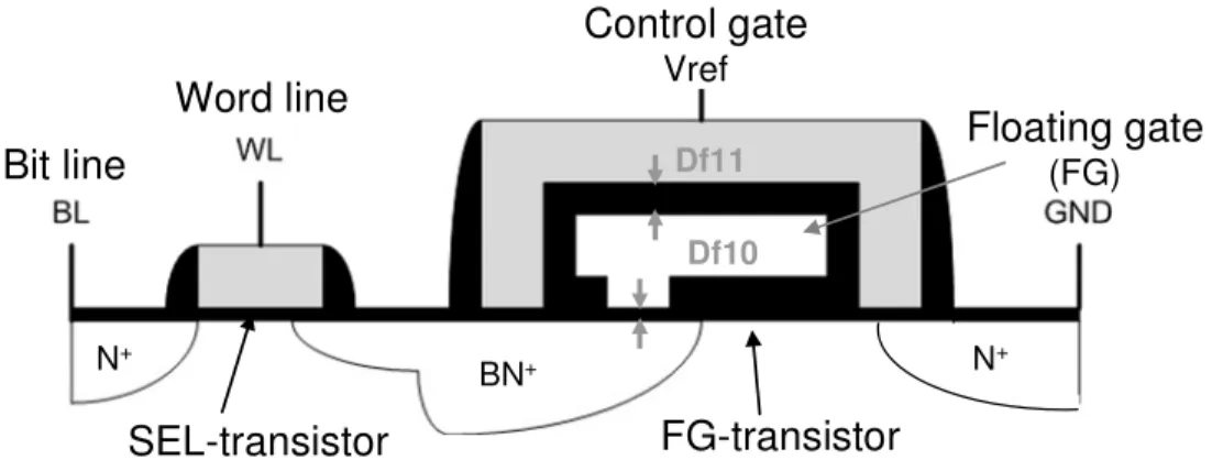
Bit Line (BLj) Word Line (WLi) Control Line (Vrefi) Source Line (Vss) SEL-transistor FG-transistor
Figure 1.3: EEPROM core cell.
Figure 1.3 presents an EEPROM core cell composed of two serial transistors. One of the two transistors is the select transistor (SEL-transistor) allowing to select the core cell from the bit-line. Note that this transistor is built with a standard NMOS transistor. The second one is the floating gate transistor (FG-transistor) that performs the memorization of the logic data [YAR82].
Unlike to the EPROM which is built with a single transistor, the EEPROM needs more area due to the presence of two transistors. Consequently, this memory is never chosen for applications that require high integration density.
1.1.2.4 FLASH
To deal with Flash memories is not an easy talk because describing this kind of memory requires to consider several parameters. Flash memories are not linked to a technology but to a structure and more precisely to a granularity. In fact, the name Flash comes from the particularity of such memory to erase a block or a page in one time. However, in almost all cases the Flash memory is built with a particular core cell technology based on a floating gate transistor. This core cell technology offers the advantage to a reduced area and can be compared to the EPROM scalability. To write a logic content in this floating gate transistor, the HEI phenomenon is used whereas to erase this core cell, the tunneling effect called Fowler-Nordheim [SHA97] is preferred. This typical Flash core cell is presented in Figure 1.4 during the write and erase operations.
Vgs>0v
Vd<Vgs Vs=0v
Hot Electrons Injection (a)
Vgs=0v
Vs>0v
Tunnelling Effect (Fowler-Nordheim) (b)
Vd=0v e
-e
Note that the Flash memory can also be built with the same core cell as the EEPROM (2 transistors) and this particular case is used for instance to design Flash memories for embedded systems.
1.1.3 FUTURE NON-VOLATILE MEMORIES
Researchers try to develop a new non-volatile memory technology taking into account all advantages from the previous described non-volatile memories (data retention, endurance …) but also from the volatile ones (high integration density, fast write speed …). Two types of memory technology seem have many of these advantages, namely the FeRAM for Ferro-electric RAM and the Phase Change RAM also called Ovonic Unified Memory (OUM).
1.1.3.1 PHASE CHANGE MEMORIES
The phase change memories (PCRAM) or OUM are one of the most interesting future non-volatile memories. The PCRAM uses the particular behavior of chalcogenide glass that can switch between two states (crystalline or amorphous) thanks to a heat application. The chalcogenide [YAM91] belongs to the same material family than that used to build re-writable optical media as CD-RW or DVD-RW. In optical media disc, a low power laser beam focuses the media to locally heat its surface and switch the material from a crystalline to an amorphous state. This phase change from a crystalline to an amorphous state corresponds to a binary data. The difference between these two states is sensed in an optical way based on the reflectivity behavior of the memory point which is either written or erased. In the PCRAM the principle of erasing and writing the core cell is different because the logic data corresponding to the material state is obtained electrically. In fact, the PCRAM undergoes a phase change (crystalline to amorphous) due to a current passing through the material and involving a joule effect. This kind of core cell is represented by a cross-section scheme in Figure 1.5. Before the joule effect, the material has a low resistance whereas after the joule effect, the material has a high resistance value due to its amorphous state. To switch the material from one state to the other, it takes less than 30ns and some prototypes built by Samsung Company achieve a phase change speed close to 5ns.
Top Electrode Polycrystalline Chalcogenide Heater Bottom Electrode Programmable Volume
Figure 1.5: Cross section of a PCRAM core cell.
To forecast the endurance of a PCRAM core cell a lot of cycling tests have been carried out by researchers and have shown that after 1012 cycles the resistance value of the material is almost unchanged. Note that this endurance has never been achieved with other non-volatile memories. Since 2001, research teams develop phase change memories prototypes [LAI01] [GIL02] and they are facing two main problems which are the programming current reduction and the design of high density array. Currently, a few companies begin to design PCRAM array containing more than 512Mbits.
1.1.3.2 FERAM
The Ferroelectric RAM (FeRAM) cell is designed with the same elements as those widely used DRAM cells, namely the access transistor and the cell capacitor. Note that this cell structure is called 1T-1C. In a DRAM, the cell capacitor is built with a linear dielectric whereas in FeRAM, the cell capacitor is based on a dielectric structure including ferroelectric material, typically Peroveskite Zirconate Titanate (PZT). Figure 1.6 describes the FeRAM core cell.
Bit Line
Word Line
CFE
Figure 1.6: 1T-C FeRAM core cell.
Operationally, a FeRAM is similar to a DRAM. To write the FeRAM cell, an electric field is applied across the ferroelectric layer by charging the plates on each side of it. The presence of the electric field forces the atoms inside into a up or down orientation according to the polarity of the charge applied and thereby a binary information can be stored, a logic ‘1’ or ‘0’. Reading the
FeRAM cell is different than reading a DRAM cell because thanks to the access transistor, the FeRAM cell is forced into a particular state, called ‘0’. If the FeRAM cell already contains a logic ‘0’, nothing occurs at the output lines. If the cell contains a logic ‘1’, the re-orientation of the atoms in the material causes a brief pulse of current through the output line as they push electrons out of the metal on the down side. The presence of this pulse is sensed and interpreted as a logic ‘1’. Moreover, the read operation has to be considered as aggressive because after this operation, if the FeRAM cell contains a logic ‘1’, this value will be over-written and replaced by a logic ‘0’. To repair the read operation the FeRAM cell rewrite to a logic ‘1’ has to be performed. However, note that in a FeRAM memory, write and read operations are quite similar to DRAM. In a near future, due to its high integration density, to its fast write and read speed but also to its high endurance and data retention characteristics, the FeRAM could be very interesting.
1.2 NON-VOLATILE MEMORY TECHNOLOGY
The non-volatile memory principle is to keep data information without any electrical supply voltage. Researchers have found a lot of solutions to develop non-volatile memory core cells that are compliant with CMOS technology. The most known solutions are based on electrical charges storage for modulating the electrical characteristics of a custom transistor such as its threshold voltage value. For instance, if two different threshold voltage values are reached in a transistor two different logic states are obtained, a logic ‘1’ or a logic ‘0’. Then, thanks to a particular polarization these two states are sensed in an electrical way. Currently, there are two charge storage technologies for non volatile memories [BRO98], the floating gate technology and the charges trap technology. In the near future, other type of storage technology for non-volatile memory, like the ferroelectric technology mentioned in the previous section, will be possibly used in production.
1.2.1 FLOATING GATE TECHNOLOGY
The floating gate principle is to catch electrical charges into an isolated gate of a double gate MOS transistor. Note that this isolated gate, called floating gate, is built with a conductor or semi-conductor. This structure is represented in Figure 1.7. With the stored electrical charges, the threshold voltage value of the MOS transistor is modulated. In almost all cases, charges are injected through a dielectric built with an oxide like SiO2. This oxide is located between the
floating gate and the channel of the double gate transistor. A second gate, called control gate, is placed under the floating gate and corresponds to the basic gate of a MOS transistor. These two gates are separated by a thick oxide layer called ONO (Oxide-Nitride-Oxide) [BRO98]. Programming a memory core cell built with the floating technology can be done by using two types of charges injection. The first one is the Hot Electron Injection (HEI) used by the technology SIMOS (Stacked gate Injection MOS) often used to build EPROM. In this technology SIMOS, the floating gate and the control gate are built in polysilicon [ROS77]. The floating gate of this SIMOS cell is charged by HEI and the charges are removed by performing UV beam insulation. During an HEI operation there is a consequent current consumption due to the conduction state of the SIMOS core cell. Moreover, the efficiency of the programming operation by HEI is related to the doping quantity present in the bulk, to the channel length and to the overlap size between the floating gate and the drain diffusion [BRO98].
The second mechanism allowing to program a floating gate core cell is the Fowler-Nordheim tunneling effect. This is a quantum phenomenon that allows injecting charges in the floating gate through a thin oxide of about 8 to 10nm. This programming mechanism is used for the specific FloTOx core cell (Floating gate Tunneling Oxide) in EEPROM. Note that a mixed solution is used to program ETOX (EPROM Tunnel Oxide) core cells used to build Flash memories. In this case, a HEI is performed to erase the core cells and a Fowler-Nordheim tunneling effect is performed to write the core cells.
N+ BN+
Bulk P type Poly-silicon
ONO
Drain diffusion Source line Control gate
Poly-silicon
Figure 1.7: Cross section of a basic floating gate structure
Figure 1.8 details a FloTOx structure in which the Fowler-Nordheim principle is used to inject or remove charges from and into the floating gate. This quantum charge injection principle was used initially in a non-volatile RAM core cell [HAR78] and was the first step before the
development of the EEPROM at the beginning of 80’s. The FloTOx technology can be either double or simple polysilicon but the most often used in EEPROM is the double polysilicon technology. BN+ FG-transistor SEL-transistor Control gate Word line Bit line N+ N+
Figure 1.8: FloTOx core cell with double polysilicon technology.
In the FloTOx structure built with double polysilicon technology the second polysilicon gate, called control gate, is above the floating gate and separated from this one by an oxide called ONO (Oxide Nitride Oxide). Whatever the technology used to build FloTOx core cells, there is always a tunnel window in which the oxide is thinner (8 to 10nm) in the oxide between the floating gate and the channel. Electrons go through this thin oxide layer tanks to the tunneling effect when an electric field is applied between the floating gate and the drain diffusion. According to the value of the electric field, electrons are injected or removed into and from the floating gate. Hence, this charge quantity increases or decreases the threshold voltage value of the FloTOx core cell.
1.2.2 CHARGE TRAP TECHNOLOGY
In this section, the non-volatile memory technology based on the charge traps principle in insulator is described. There are two main memories built with this particular technology namely the MNOS and SONOS memories [SHA97].
1.2.2.1 MNOS TECHNOLOGY
Concerning the MNOS (Metal Nitride Oxide Semiconductor), instead of storing electrical charges in a floating gate, charge traps situated in a nitride layer are used. The electrons are injected through a thin oxide layer of about 1.5nm to 3nm thickness thanks to a tunneling effect. Once the electrons are trapped, the threshold voltage value of the MNOS core cell is modified.
Figure 1.9 describes an EAROM core cell (Electrically Alterable semiconductor ROM) in MNOS technology. Like basic transistors, this EAROM core cell has a control gate in metal. The charges are injected through the central oxide layer between the channel and the nitride layer Si3N4.
However, this kind of non-volatile memory core cell features some drawbacks, such as its low speed, its limited density and the using of several electric potentials to run it.
Si3N4 Gate in Al P+ P+ SiO2 N type bulk
Figure 1.9: EAROM core cell based on MNOS structure.
In the 80’s, the MNOS technology has been improved with the SNOS technology (Silicon Nitride Oxide Silicon) based on the LPCVD (Low-Pressure Chemical Vapor Deposition) method that stacks the polysilicon on the nitride layer and the pre-metallization by an hydrogen annealing at a high temperature to enhance the nitride to thin oxide interface [BRO98].
1.2.2.2 SONOS TECHNOLOGY
The SONOS (Silicon Oxide Nitride Oxide Silicon) technology has been developed in order to reduce the charge injection from the gate to the nitride compared to the MNOS technology. An oxide layer of about 2nm to 3nm is introduced between the nitride and the polysilicon gate [CHE77]. This oxide layer is obtained by nitride oxidation, thus reducing its thickness. However, this nitride thickness reduction involves a hole leakage to the gate. In fact, as the trapping length in the nitride is higher for holes (15 to 20nm) than for electrons (5 to 10nm), reducing the nitride thickness (<20 nm) makes that the holes are trapped at the nitride to gate interface whereas the electrons are caught in the nitride. Several holes are lost through the gate even in presence of a thin oxide layer between the nitride and the gate. This involves a decrease of the threshold voltage value.
SiO2 Si3N4 SiO2 Polysilicon
a b
Figure 1.10: SONOS technology comparison between the old (a) and the new SONOS concept (b).
To avoid this trapped holes leakage through the gate, there is a new concept of SONOS structure keeping the same specificities [SUZ83] [CHA87] [DEL87]. This new concept of the SONOS structure layers is presented in the right part of the Figure 1.10. This new structure is thus composed by a thin oxide layer, a thin nitride layer (<10nm) and a thicker oxide layer (>3nm) [SUZ83] [DEL87]. These new characteristics allow to considerably reduce the SONOS structure thickness (Figure 1.10) and thus the necessary programming voltage (<5V). Moreover, the retention and the structure reliability are enhanced.
1.3 EMBEDDED FLASH (EFLASH) MEMORIES BUILT WITH FLOTOX CORE CELLS 1.3.1 EFLASH MEMORIES ARCHITECTURE
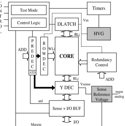
The functional scheme of an eFlash memory is presented in Figure 1.11. Like all other memories, the eFlash is composed of a core cell array (CORE), data latches (DLATCH), bit-line and word-line decoders and sense amplifiers. In addition, eFlash memories need two particular building blocks to perform dedicated functions: a Charge Pump device for the High Voltage Generation (HVG) allowing the write and erase operations and a Sense Reference Voltage used during the read operation.
Two types of core cell array can be used to realize an eFlash memory; NOR and NAND-based structures [SDC91]. Here, only the NOR-NAND-based structure is presented as this is the most often used structure in high-speed applications. In a NOR-based eFlash, core cells are placed in parallel as shown in Figure 1.12. A word-line (WLi) is shared by all the cells in the row. All the cells of one row are addressed together to form a page.
CORE R O W D E C P R E D E C ATD DLATCH Y DEC
Sense + I/O BUF Test Mode Control Logic Timers HVG Redundancy Control Sense Reference Voltage I/O WLi BLj Vsense ADD atd Margin mgm analog BLj Vm C O N T R O L ADD
Figure 1.11: Functional scheme of eFlash memories
WLi-1 Source line (Vss) WLi Source line (Vss) WLi+1 Source line (Vss) WLi+2 Source line (Vss) BLj-1 BLj BLj+1 BLj+2
Figure 1.12: NOR eFlash structure
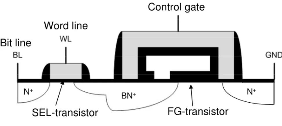
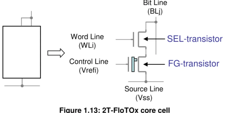
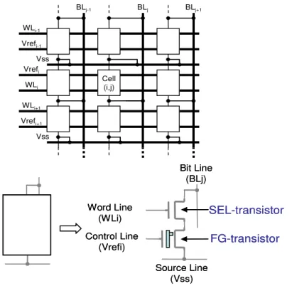
The eFlash core cell is based on the floating gate (FG) concept. As discussed previously, there are two typical mechanisms to transfer electric charges from and into the FG: hot carrier injection (HCI) [SHA97] and the Fowler-Nordheim (FN) tunneling effect [SHA97]. The FN tunneling effect is used for charge injection or removal in FloTOx core cells. In our work, we consider the FloTOx core cell structure presented in Figure 1.13 [SDC91] [SHA97]. The memory
cell is composed of a select transistor (SEL-transistor) and a floating gate transistor (FG-transistor). The SEL-transistor having the word line connection (WL) allows the selection of the targeted cell. It also avoids disturbances from the high voltage on the bit-line when the cell is not selected. The FG- transistor contains the floating gate (FG) and the control gate.
Bit Line (BLj) Word Line (WLi) Control Line (Vrefi) Source Line (Vss) SEL-transistor FG-transistor
Figure 1.13: 2T-FloTOx core cell
1.3.2 EFLASH MEMORY FUNCTIONING
Three different operations can be performed on an eFlash: Erase, Write and Read. In the following, the cell(i,j) in the NOR-based array in Figure 1.12 is considered as the target cell. The different voltage levels required for the erase, write and read operations of cell(i,j) are reported in Table 1.1. The Erase operation consists in injecting charges in the FG with a specific high voltage combination. To inject charges in the FG, the high voltage must be applied on the Vrefi node of the sense transistor while its drain must be maintained at ground. During the Erase operation, the core cell is 'on' and allows the node BLj to be pulled-down at the Vss potential.
ERASE WRITE READ
BLj 0v Vpp 1v BLx 0v HZ HZ WLi 15v 15v 3.3v WLy 0v 0v 0v Vss 0v 1.2v 0v Vrefi Vpp 0v 0.7v Vrefy HZ HZ HZ
with x≠j and y≠I Vpp ≈ 12.5v
Table 1.1: Voltage levels for Erase, Write and Read operations
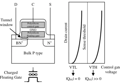
At this point, it is important to notice that the erase operation is performed simultaneously on all the cells of the same page, equivalent to all core cells belonging to a word line, and not cell by cell. At the end of the erase operation, charges in the FG have changed the VT of the sense transistor to a high VT (VTH in Figure 1.14). From a functional point of view VTH corresponds to logic '1'.
The Write operation consists in removing charges from the FG by putting the Vref node at ground while maintaining BLj at a high voltage (see Table 1). With this operation, charges of the FG are removed and so, the sense transistor has a low VT (VTL in Figure 1.14) which corresponds to logic '0'. The difference between VTH and VTL is called VT window.
As for all other kinds of memory, the read operation is performed by a sense amplifier but this time working in a current measurement mode. The Vref node is set around 0.7v during the read operation (see Table 1.1). If the sense transistor has a low VT (VTL), it delivers a current (between 10µA to 30µA) and the sense amplifier provides a logic '0' on its output. On the other hand, with the same Vref value, if the sense transistor has a high VT (VTH) there is no current through the bit-line and hence the sense amplifier gives a logic '1'.
Se ns e th re sh ol d D ra in c ur en t Control gate voltage VTL VTH |QFG| = 0 |QFG| >> 0 N+ BN+ Bulk P type Polysilicon control gate ONO D C S Charged Floating Gate Polysilicon floating gate Tunnel window
Figure 1.14: VT modulation with charge quantity
1.4 CONCLUSION
In this first chapter an overview of volatile and non-volatile memories has been presented. All these memories have several specificities and characteristics and allow to cover a large panel of electronic systems and applications. To summarize this overview, Table 1.2 presents a summary of embedded RAM and embedded Flash memories performances and, in Table 1.3 there is a characteristics comparison between actual Flash memories and future non volatile memories.
The unique memory able to be used in all of electronics systems does not exist yet and researcher work hardly in this field. Moreover, this chapter has introduced the context of our work which is related to embedded Flash memories (eFlash) built with FloTOx core cells. Due to its low access time, low power consumption and to its high density, this kind of non-volatile
embedded memory is popular for portable devices. However, the high integration density of the eFlash memories and their particular process steps make them more and more prone to inter or intra core cell defects that will be analyzed in the next chapter.
eDRAM eSRAM eFLASH
Cell size 25-30F2 120-140F2 15-30F2
Extra masks +5 0 +10-12
Read Speed Up to 200MHz
(4Mbits&90nm) Up to 1GHz (512Kbits&90nm) Up to 50MHz (4Mbits&90nm)
Comments Large amounts of cache to
justify process cost Large overhead
Leakage issue requiring process options (VT, Tox) for potable applications
Low speed programming
Potential issues Leakage
Stack capacitance value Leakage SNM Soft errors: SEU
Tunnel oxide Leff scaling with HEI Gate coupling Solutions to push the limits High K materials MIM cap ECC Design techniques ECC materials 3D structures High K materials Design techniques ECC ITRS prospects (2015) Cell size: 0.0038µ2 Up to 10Gbits
Cell size: 0.15µ2 Cell size: 0.013µ2
Table 1.2: Summary of embedded RAM and Flash performances
Flash MRAM FeRAM PCRAM
Current status Cell size Write time Mask count(*) Endurance Maturity 2.3-40F2 µs +5-10 105-106 130nm Volume Prod 20-60F2 <100ns +2-4 >1014 180nm Test chips 15-200F2 <100ns +2-3 1010 Limited prod 0.35um 12-40F2 <100ns +5-6 1012 Test chips Scalability FAIR Down to 45nm ?? ?? Good R&D SONOS Nanocristal Improve scalability and write time
TAS CIMS Improve scalability 1T,1C stacked cell, 2D-3D FeCAP Improve scalability Decrease reset current Materials
(*) depends on technology and high voltage requirements, does not reflect automatically the process complexity (MTJ stack complexity on MRAM for example)
2
C
HAPTER2:
G
ENERALA
SPECTS ONM
EMORYF
AULTM
ODELING ANDT
ESTINGIn the previous chapter, we have seen that stand alone memory market increases drastically and that embedded memory resources are continuously increasing and will approach 94% of the System on Chip (SoC) silicon area in the next ten years [SIA03]. These statements highlight the main issue that we are currently facing in the field of memory design and test. In fact, because of their high density, memories are considerably impacting test time and for the embedded ones they are becoming the main contributor of the overall SoC yield loss. Consequently, efficient test solutions and repair schemes for these memories are needed. This chapter proposes a summary of existing state of the art solutions for memory testing. Special interest will be given to eFlash memory testing.
2.1 BACKGROUND OF RAM FAULT MODELING AND TESTING
The high integration density of memories and their particular manufacturing process steps make them more and more prone to defects. Memory device failures can be classified according to three families [SHA97]:
• the infant mortality failures associated to designs errors or to process defects and to bad process steps during the production flow,
• the usage failures caused by a reliability missing, an electro-migration phenomenon or a perturbing event like a SEU (Single Event Upset),
• the wear-out failures due to operational conditions, to the aging effect of electrical contacts for instance or to mechanical stress during the device use.
To detect these failures in integrated circuits or systems, the use of comprehensive fault models is required and adequate stimuli to detect these faults have to be found. Note that fault models can be defined according to different abstraction levels as behavioral, functional, structural or electrical description levels. From a memory modeling point of view, the functional
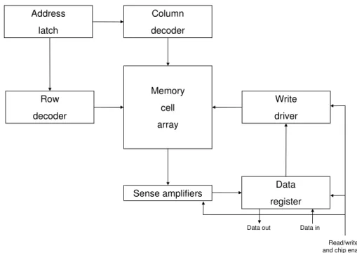
scheme of a RAM (Figure 2.1) can represent almost all semiconductor memories because the operations performed are always the same, i.e. writing a data in a core cell, storing a data or providing a data read-out from a random core cell location.
Address latch Column decoder Row decoder Memory cell array Sense amplifiers Write driver Data register Data out Data in
Read/write and chip enable
Figure 2.1: Functional scheme of a RAM chip.
2.1.1 RAM FAULT MODELS
In semiconductor memories and more especially for the RAM family, several types of physical faults can appear in a chip. Based on the general memory scheme described in Figure 2.1, we can expect to observe functional faults in different parts of a memory device:
• Cells stuck, a memory cell storing a binary value can be stuck to a logic ‘0’ or to a logic ‘1’.
• Read/write lines stuck, the lines driving the read or write signals can be stuck to a logic value ‘0’ or ‘1’ so that inhibits the read or write operations.
• Chip select line stuck, the signal ‘Chip select’ that switch ‘on’ the memory device can be stuck to a logic value and thus the memory chip can be selected or unselected every time.
• Wrong memory access, this fault induces a decoding problem in the address decoder logic and access problems occur during the write or read operation performed on victim memory cells.
This functional fault description is not enough to test precisely memory device like RAM and this is the reason why a logical fault modeling has to be performed. This modeling allows not only to test memories but also to examine precisely the physical causes of the fault based on a logical comparison with the known good dies. Note that a physical examination of the fault in a memory is not always easy due to the high cost of examination process and equipments.
In the RAM testing literature [VAN00] [ALA01], there are two main families of fault models. The first family relates to a static faulty behavior whereas the second relates to a dynamic faulty behavior.
* Static faults are sensitized with only one operation (read/write). The most known fault of
this family is the simple Stuck-At Fault (SAF) model that can alter the content of a core cell. For instance, imagine that a core cell Cx is Stuck-At zero (SAF0). This means that irrespective of the operation acted on cell Cx, its contents will remain at ‘0’. To sensitize this fault, only one operation has to be applied, a write ‘1’ in the faulty core cell. In fact, at the end of the write ‘1’ operation, the core cell has not flipped from a logic ‘0’ to a logic ‘1’, as expected. To observe the result of the write ‘1’ operation, a read ‘1’ of the core cell Cx is needed and due to the SAF0 the expected ‘1’ will never be read.
This family includes some type of other fault with a faulty behavior that can be harder to detect. There are the Address decoder Faults (AFs) present in the address decoder circuitry of a memory chip. In this fault model several combinations of addresses are possible at the same time, involving multiple core cells to be addressed simultaneously. There are also fault models involving a unique core cell at a time, like the Stuck-At Faults (SAFs), the Stuck-Open Faults (SOFs), the Transition Faults (TFs) or the Data Retention Faults (DRFs). Then, there are the fault models describing a coupling phenomenon between two core cells, an aggressor and a victim. This sub-family includes the so called Coupling Faults (CFs).
Note that the static fault models can be more complex if we consider for example that two coupling faults with two different aggressor core cells can be linked and affect the same victim core cell. The faults that occur in this configuration are called Linked Static Faults.
* Dynamic faults are sensitized with at least two operations (read/write). These faults are
harder to detect compared to the previous static faults because they appear after a particular sequence of read/write operations performed on the memory cells. These faults are currently among the main problematic in the field of RAM fault testing and a lot of research works have
been done to primarily address the problem of dynamic fault modeling [BOR05]. The well known dynamic fault models are the Address Decoder Open Faults (ADOFs), the dynamic Read Destructive Faults (dRDFs), the dynamic Data Retention Faults (dDRFs), the Un-Restored Write Faults (URWFs) and the Un-Restored Read Faults (URRFs).
To illustrate this particular fault family, the most known dynamic fault, called dynamic Read Destructive Fault (dRDF), is described. First of all let us consider the definition of dRDFs established by [VAN00]:
• A cell is said to have a dRDF if a write operation immediately followed by a read
operation performed on the cell changes the logic state of this cell and returns an incorrect value on the output.
To well understand this particular fault, the analysis of what are their probable origins is required. In [DIL05] an exhaustive analysis of actual resistive open defect occurring in an SRAM core cell has been carried out. In this work, authors shown that a particular location of a resistive open defect in an SRAM core cell could impact the logical core cell behavior and can be modeled as a dRDF. Moreover, the author showed that according to the resistive open values, the number of read operations (read destructive) required to change the logic state of the cell, is different. This statement confirms that such resistive defect configuration involves a dynamic fault.
As explained previously, dynamic faults such as dRDF are harder to test than static faults due to their nature and particular behavior. They are currently the main problematic in RAM testing.
2.1.2 RAM TEST ALGORITHMS
In the previous sections the various fault models available for memories, especially for RAM. In this section we deal with methods to test these fault models. Remember that a memory is a particular chip having a large quantity of internal states related to its size, i.e. 2n with n the number of bits in the memory. Because of time constraints, the test of all possible internal states of memory is not possible. Currently, memories achieve more than 1Gbits of storage capacity. For instance, with a O(n2) test procedure, a 4Mbits SRAM would be tested in 500 hours. Thus, based on their regular structure and on their functional fault models, researchers have developed new test methods and algorithms with a O(n) complexity.
writing in all the memory chip. In this test category, there are the Checkerboard Pattern and its inverse used to test direct shorts between topological adjacent core cells. There are other patterns like Column Bars or Row Bars. Although simple to implement and test time advantageous, these patterns present a low fault coverage and only the SAF detection is guaranteed [VAN98a].
For these reasons researchers have developed new methods, called March tests, achieving a high coverage for SAF, TF, AF or CF. March algorithms have a low complexity (O(n)) and more flexibility thanks to their Degree of Freedom (DOF) [NIG98]. We assume the definition of a March test described by [SUK81]:
A March test consists of a finite sequence of March elements. A March element is a finite sequence of operations applied to every cell in memory before proceeding to the next cell. The latter can be done in either one of two address orders: an increasing (
⇑
⇑
⇑
⇑
) address order (e.g. from address 0 to address n - 1), or a decreasing (⇓
⇓
⇓
⇓
) address order which is the opposite of the⇑
⇑
⇑
⇑
address order. When the address order is irrelevant the symbol ↕ is used. An operation can consist of: writing a ‘0’ into a cell (w0), writing a ‘1’into a cell (w1), reading a cell with expected value ‘0’ (r0), and reading a cell with expected value ‘1’ (r1). Note that all operations of a March element are performed at a certain address, before proceeding to the next address.
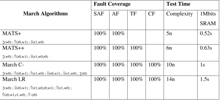
To illustrate the definition of March test algorithms, the well known March C- [MAR82] used by several semiconductor companies to test RAM is described. This is a 10N linear test, which is effective to detect Stuck-At Faults, Transition Faults and Coupling Faults. March C- has the structure shown in Figure 2.2.
↕(w0) ; ⇑(r0,w1) ; ⇑(r1,w0) ; ⇓(r0,w1) ; ⇓(r1,w0) ; ↕(r0)
Figure 2.2: March C- structureHowever, to test each kind of fault model described previously, a March test must satisfy certain conditions. For instance, to build a March test allowing to detect a Transition Fault <↑/1>, a particular sequence of predefined elements has to be implemented. Let us consider the state diagram presented in Figure 2.3 and Figure 2.4, the first diagram shows the good behavior of a memory cell whereas the second scheme describe a memory cell presenting a Transition Fault <↑/1>.
S0
S1
w0
w1
w0
w1
Figure 2.3: State diagram of a fault free SRAM core cell.
S0
S1
w0
w0
w1
Figure 2.4: State diagram of a faulty SRAM cell presenting a TF.
By looking at these two state diagrams, we can easily develop the particular sequence to implement in the March algorithm in order to detect a TF <↑/1>:
• (…, w1,r1, …)
Indeed, the presence of a TF<↑/1> on a victim memory cell can be detected by performing a write ‘1’ on the victim cell immediately followed by a read ‘1’ operation of the same cell. So that all TF<↑/1> are detected, the element (…, w1,r1, …) must be in the March test algorithm. Note that the dots (…) correspond to any operation before and after the element “w1, r1” detecting the TF<↑/1>. For each fault model like Stuck-At, Coupling Fault, etc…, we have to reproduce the same reasoning as for the TF<↑/1> and find elements to implement March test algorithm.
Table 2.1, presents a list of four March algorithms with their respective fault coverage for SAF, AF, TF and CF. We have also given the test time if we apply each algorithm in a 1Mbits SRAM.
Fault Coverage Test Time
March Algorithms SAF AF TF CF Complexity 1Mbits SRAM MATS+ ↕(w0) ; ⇑(r0,w1) ; ⇓(r1,w0) 100% 100% 5n 0.52s MATS++ ↕(w0) ; ⇑(r0,w1) ; ⇓(r1,w0,r0) 100% 100% 100% 6n 0.63s March C- ↕(w0) ; ⇑(r0,w1) ; ⇑(r1,w0) ; ⇓(r0,w1) ; ⇓(r1,w0) ; ↕(r0) 100% 100% 100% 100% 10n 1s March LR ↕(w0) ; ⇓(r0,w1) ; ⇑(r1,w0,r0,w1) ; ⇑(r1,w0) ; ⇑(r0,w1,r1,w0) ; ⇑ (r0) 100% 100% 100% 100% 14n 1.5s
Table 2.1: Comparison of four different March algorithms.
2.2 BACKGROUND OF FLASH MEMORY FAULT MODELING AND TESTING
Exploiting their similarities with RAM, some fault models have initially been adapted to Flash memories [SHA97]. As there are structural differences between RAM and Flash memories, all RAM fault models are not realistic transposed in a Flash context. Only four main fault models can be found in the Flash test literature: the Stuck-At Fault model, the Transition Fault model, Address decoder Fault and State Coupling Fault. Note that certain Coupling Fault models like the Idempotent Coupling Fault model are not present due to the specificities of Flash memories allowing to avoid such faults. In this field, there is only few research works dealing with Flash fault modeling as well as Flash testing.
2.2.1 THE 7-PATTERNS TEST SEQUENCE
To test their Flash memories, semiconductor companies exploit several functional patterns which exercised the chip to detect any address sequencing and data pattern sensitivities. In the literature we often find the most known 7-patterns sequence allowing to test Flash memories (or EEPROM) like a Static RAM by performing the following programming (erase and write) and read operations:
• Write all 0s and Read all 0s – This pattern ensures the operability of the EEPROM or Flash memory page mode. Moreover this pattern preconditions the memory for the next pattern, i.e. GalPat0.
Thanks to the GalPat0 the read disturbances is tested between byte or word by reading “00” alternately in byte or word sharing the same column or row.
• Bit Checkerboard –At first, a succession of ‘0’ and ‘1’ is written to obtain an opposite state between two adjacent core cells in the memory array. Then, there is a second pattern corresponding to the complement of the previous one. The Bit Checkerboard pattern ensures that every cell can be written to a ‘1’ or ‘0’ but also that the adjacent core cells which are written with an opposite state do not affect the state of the cell under test.
• Columns Pattern – This pattern writes alternating columns composed of a byte or a word with “00” and “FF” to precondition the memory for the next pattern.
• DRAD (Diagonal Read of Alternating Data) – During the DRAD, no write operations are performed but only read operations. Indeed, in this pattern only the bytes or word belonging to the memory array diagonal are read. This configuration is extreme because for each read cycle the address decoders change and the data read is the complement of the previous one. Moreover, this pattern is often used for AC parametric test because it corresponds to the worst case of read access time.
• Bit unique test – This pattern verifies that every bit within a byte is unique and ensures that two bits are not shorted
• March element – Based on a byte or word write operation granularity, this pattern writes a March algorithm element in the entire Flash or EEPROM memory chip. Considering the March LR algorithm, this March element pattern could be executed using the element ⇑(r1,w0,r0,w1) . However, as the Flash or EEPROM granularity is
byte even word, the March element is performed with a data background “FF” or “00” instead of ‘1’ and ‘0’ respectively. The March element is used to test address uniqueness and multiple selections.
The functional Flash test based on a 7-patterns sequence is time consuming. To reduce test time, some special functions allowing the mass (parallel) chip erase/write modes have been implemented in Flash or EEPROM. However, these particular programming modes present some limitations in the detection of CF for example due to the limited number of combinations performed in one time. Moreover, due to the particular address decoder configuration and to the electrical features required during these parallel programming modes, some new failures
mechanisms can appear. To avoid this type of problematic, accurate electrical characterizations and estimations of these modes have to be performed.
2.2.2 THE 5-STEPS TEST SEQUENCE
From a test point of view, because of the intrinsic very low speed of programming operations, Flash memories are very different from other types of memories. Only a very limited number of patterns can be used to test Flash memories in order to keep the testing cost acceptable. Assuming a Functional Write mode (FW) with 2ms to erase and 2ms to write, it takes 4ms to program a data in a word. Note that almost all Flash memories have also a Page Write mode (PW) allowing to program a page in the same duration than for a FW.
For instance, if we consider a 256 bytes per page architecture, 512 pages are necessary to build a 1Mbits memory. Using a Page Write (PW) mode, close to 2 seconds are mandatory to write one pattern to the 1Mb Flash. Consequently, programming a set of basic patterns such as “00”, “FF”, checkerboard and inverse checkerboard using PW mode will result in a testing time close to 10s per die. Decreasing the testing time per die is technology dependent, as parallel access to full or large portions of the array is possible to speed up the programming of test patterns. Programming a huge number of cells in parallel is only possible if a very low current programming mode such as FN tunneling is used. This is the case in embedded Flash (eFlash) built with FloTOx core cells. By executing dedicated test modes, a one time programming of large sectors to “00” or “FF” is possible in a few milliseconds. A Checkerboard pattern can also be programmed in a few ms using a Concurrent Chip Write Pattern (CCWP) that allows programming in one time the data loaded in the Flash page buffer in several memory blocks. For the Checkerboard pattern, the CCWP selects either odd pages or even pages to program in one time and reduces the global programming time. In any case, even if only one test pattern is programmed using the user mode (FW), testing time of medium to large Flash memories will be in the range of seconds, to compare with milliseconds in ROM testing.
In many companies, a 5-steps test sequence is typically used to test eFlash memories. From an algorithmic point view, the 5-steps testing flow is composed as follows:
• 1st step: WCCWP CKI + Read CKI
• 2nd step: WFW CKB + Read CKB
• 4th step: CE + Read all ‘1’ • 5th step: CW + Read all ‘0’
Note that CKB (CKI) stands for checkerboard (inverse checkerboard), and Diag0 is a diagonal pattern of ‘0’. WCCWP is a test mode allowing high speed programming of the CKB
(CKI). Chip Erase (CE) and Chip Write (CW) are specific test modes allowing one time programming of the full array to ‘FF’ and ‘00’ respectively. WFW is the Functional Write mode
which corresponds to the user mode.
The fault coverage analysis of this 5-steps sequence is summarized in the last section of this chapter but we can anticipate that this kind of sequence can reach a good coverage to test Stuck-At Faults, Stuck-Open Faults, Addressing decoder Faults and Transition Faults. But due to the particular programming mode used during 5-steps test sequence, the difficulty to detect more complex faults can be easily imagined. Indeed, the writing of a large amount of cells in parallel does not allow testing particular coupling faults. For example, we can imagine that all combinations of State Coupling Faults (SCF) are not detected by the 5-steps test sequence. Now, if we consider the 1Mbits eFlash memory architecture cited above (256 bytes on 512 pages), this 5-steps sequence will take close to 5sec to test the whole memory chip. In comparison, an SRAM memory, with the same storage capacity, is tested by a 14n March LR algorithm in 1,5s.
Such test sequence will have an impact on the test quality and cost of eFlash memories. For instance if the previously detailed complex fault model (SCF) is considered, the 5-steps test sequence presents some limitations to detect this kind of fault. In this 5-steps test sequence, the patterns CKB and CKI have the ability to detect certain SCF but these patterns do not perform all possible SCF combinations in the matrix due to the particular programming modes used. In Figure 2.5, the application of the two first patterns (CKI and CKB) from the 5-steps test is presented in a small array of 3*3 core cells.

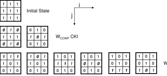
![[PDF] Cours webmaster conception et évaluation ergonomique de sites Web](data:image/gif;base64,R0lGODlhAQABAIAAAP///wAAACH5BAEAAAAALAAAAAABAAEAAAICRAEAOw==)