HAL Id: hal-00848965
https://hal.archives-ouvertes.fr/hal-00848965
Submitted on 17 Jan 2014
HAL is a multi-disciplinary open access
archive for the deposit and dissemination of
sci-entific research documents, whether they are
pub-lished or not. The documents may come from
teaching and research institutions in France or
abroad, or from public or private research centers.
L’archive ouverte pluridisciplinaire HAL, est
destinée au dépôt et à la diffusion de documents
scientifiques de niveau recherche, publiés ou non,
émanant des établissements d’enseignement et de
recherche français ou étrangers, des laboratoires
publics ou privés.
All-optical time-domain demultiplexing of 170.8 Gbit/s
signal in chalcogenide GeAsSe microstructured fibre
Sy Dat Le, Mathilde Gay, Laurent Bramerie, Thierry Chartier, Monique
Thual, Jean-Claude Simon, Laurent Brilland, David Méchin, Perrine Toupin,
Johann Troles
To cite this version:
Sy Dat Le, Mathilde Gay, Laurent Bramerie, Thierry Chartier, Monique Thual, et al.. All-optical
time-domain demultiplexing of 170.8 Gbit/s signal in chalcogenide GeAsSe microstructured fibre.
Electronics Letters, IET, 2013, 49 (2), pp.136-138. �10.1049/el.2012.4104�. �hal-00848965�
Manuscript for Review
All-optical time-domain demultiplexing of a 170.8 Gb/s
signal in a chalcogenide GeAsSe microstructured fiber
Journal: Electronics Letters Manuscript ID: Draft
Manuscript Type: Letter Date Submitted by the Author: n/a
Complete List of Authors: Le, Sy Dat; CNRS Foton, GAY, MATHILDE
Bramerie, Laurent
Chartier, Thierry; CNRS Foton, Thual, Monique
Simon, Jean-Claude; CNRS Foton,
Brilland, Laurent; Perfos/Photonics Bretange, Méchin, David; Perfos/Photonics Bretange,
Toupin, Perrine; CNRS Institut des Sciences Chimiques, Troles, Johann; CNRS Institut des Sciences Chimiques,
Keywords:
OPTICAL FIBRES, NONLINEAR OPTICS, OPTICAL SIGNAL PROCESSING, OPTICAL TIME DIVISION MULTIPLEXING, CHALCOGENIDE GLASSES, DEMULTIPLEXING
1
All-optical time-domain demultiplexing of a
170.8 Gb/s signal in a chalcogenide
GeAsSe microstructured fiber
S. D. Le, M. Gay, L. Bramerie, T. Chartier, M. Thual,
J.-C. Simon, L. Brilland, D. Méchin, P. Toupin, J. Troles
We report on four-wave-mixing-based all-optical time-domain demultiplexing of a 170.8 Gb/s signal down to 42.7 Gb/s in a chalcogenide GeAsSe microstructured fiber. The high nonlinearity of the fiber allows error-free and low power penalty operation with only 56 mW of total input average power.
Introduction: All-optical signal processing is one of the key
technologies for future telecommunication networks which require high-bit-rate data signals. The limitation of electronic bandwidth makes electronic components not suitable for bit rates higher than 100 GHz. All-optical signal processing can, not only increase the capacity, but also avoid the optical-electrical-optical conversion process. It can thus reduce the power consumption of systems. Among several all-optical functions, time-domain demultiplexing plays an important role. Several schemes have been proposed to perform all-optical time-domain demultiplexing. They can be based on nonlinear effects in highly-nonlinear fibers (HNLF) [1], waveguides [2], silicon nanowires [3], or nonlinear optical loop mirrors [4], etc. Devices based on four-wave mixing (FWM) [1-3] offer a potential for ultrafast operation owing to the femtosecond response time of the Kerr nonlinearity. The key parameters of nonlinear devices used for demultiplexing are the nonlinear coefficient, the loss and the dispersion. These parameters must match the specifications of demultiplexers which are in general low power consumption, high bandwidth and compactness. Due to their recent growth, chalcogenide microstructured fibers [5] offer now a great potential to implement all-optical signal demultiplexing at high bit rate.
In this letter, we experimentally demonstrate, for the first time to our best knowledge, all-optical demultiplexing of a 170.8 Gb/s on-off-keying signal in a chalcogenide GeAsSe microstructured fiber with a total average power of 56 mW and low power penalties. The performances of the demultiplexer in terms of power and penalty are comparable or better than the state of the art. Fiber characterization is firstly described. The demultiplexing experiment is then presented.
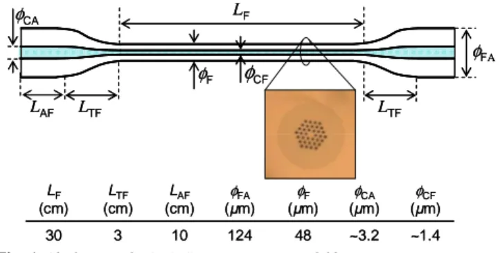
Chalcogenide microstructured fiber: The fiber is fabricated by the
casting method described in Ref. [6]. The composition of the glass is Ge10As22Se68. The structure of the fiber is designed with three rings of
holes around a solid core as seen in Fig. 1. The fiber is fabricated with a core diameter as small as possible to enhance the nonlinear coefficient
γ, while the core diameter of input and output ends is kept larger to reduce the coupling loss. The geometrical parameters of the fiber are summarized in the table of Fig 1.
10 LAF (cm) 3 LTF (cm) ~1.4 ~3.2 48 124 30 φCF (µm) φCA (µm) φF (µm) φFA (µm) LF (cm) 10 LAF (cm) 3 LTF (cm) ~1.4 ~3.2 48 124 30 φCF (µm) φCA (µm) φF (µm) φFA (µm) LF (cm) LTF LF φFA φF LTF
φ
CF φCA LAF LTF LF φFA φF LTFφ
CF φCA LAFFig. 1 Chalcogenide GeAsSe microstructured fiber.
The fiber is drawn with a core diameter of only 1.4 µm on a length LF
of 30 cm. The external diameter φF is 48 µm. The fiber loss is measured
to be 0.9 dB/m. Based on self-phase modulation (SPM) as well as FWM experiments, the nonlinear coefficient γ and the group-velocity dispersion D are evaluated to be 25 000 W−1km−1 and −310 ps/km/nm, respectively. These values of length and dispersion allow us to reduce
the temporal walk-off between two pulses propagating in the fiber at different wavelength and experiencing the fiber dispersion.
Experiment and results: Fig. 2(a) illustrates the experimental setup for
the generation of both the 170.8 Gb/s signal and the 42.7 GHz signal and Fig. 2(b) represents the FWM-based demultiplexing setup.
1 nm VA EDFA PC EDFA GeAsSe fiber Free-space Coupling Free-space Coupling PC 170 Gb/s 42.7 GHz Rx 3 nm EDFA POF 8 nm EDFA 3.5 nm MZI PRBS MUX 42.7→170 EDFA 3 nm 170 Gb/s 42.7 GHz 3 dB coupler EDFA QD-MLLD MZI CW Electrical Clock 42.7 GHz ∆
τ
20 m SMF (a) (b)Fig. 2 Experimental setup of 170.8-to-42.7 Gb/s demultiplexing: (a) generation of the data clock signals and (b) FWM experiment.
Firstly, a 42.7 GHz optical clock signal is generated at a wavelength of 1535 nm by a LiNbO3 Mach-Zehnder interferometer (MZI) from a
continuous wave laser and a 42.7 GHz electrical clock signal. It is then injected in the cavity of a quantum-dash mode-locked laser diode (QD-MLLD) through an optical circulator to generate a 42.7 GHz optical clock signal centered at 1553 nm. The spectrum of this clock signal is as broad as 13 nm, allowing thus its tunability by using a tunable filter. To compensate the chirp induced by the laser, a 20-m-long single-mode fiber is used to obtain Fourier-transform-limited pulses. The 42.7 GHz optical clock signal is amplified and then divided into two parts by a 3 dB coupler. One part is filtered by a 3.5 nm Gaussian filter centered at 1556.2 nm and encoded with a pseudo-random bit sequence (PRBS) of 27−1 pattern length by a second LiNbO3 MZI. It is then optically
time-division multiplexed to generate the 170.8 Gb/s data signal. The second part of the 42.7 GHz signal is passed through a 3 nm filter centered at 1550.8 nm and an optical delay-line (∆τ).
Wavelength (nm) In te n s it y (a .u .) 1545 1550 1555 1560 -50 -45 -40 -35 -30 -25 -20 -15 Wavelength (nm) In te n s it y (a .u .) 1545 1550 1555 1560 -50 -45 -40 -35 -30 -25 -20 -15 42.7 Gb/s demux 1545 1550 1555 1560 -50 -45 -40 -35 -30 -25 -20 -15 Wavelength (nm) In te n s it y (a .u .) 170 Gb/s 42.7 GHz 1545 1550 1555 1560 -50 -45 -40 -35 -30 -25 -20 -15 Wavelength (nm) In te n s it y (a .u .) 170 Gb/s 42.7 GHz (a) (b) 10 30 50 70 90 0 20 40 60 80 Time (ps) P o w e r (a .u .) 1 2 3 4 10 30 50 70 90 0 10 20 30 40 50 60 70 80 90 0 20 40 60 80 Time (ps) P o w e r (a .u .) 1 2 3 4 (c)
Fig. 3 Spectra at the input (a) and at the output (b) of the GeAsSe fiber, and (c) input eye-diagram of both 170.8 Gb/s and 42.7 GHz signals.
As illustrated in Fig. 2(b), both signals are then amplified by erbium-doped-fiber amplifiers (EDFAs) and aligned in polarization by polarization controllers (PCs). A programmable optical filter (POF) is used to filter and to compensate for the residual chirp of both signals. It is also used as a coupler to combine both signals. To reject the amplified spontaneous emission (ASE) noise due to amplifiers, a tunable filter with a bandwidth of 8 nm is used. The power launched into the fiber is adjusted by an optical variable attenuator (VA) just before the fiber. To perform light coupling in the chalcogenide fiber, microlensed fibers with a mode field diameter of 3.1 µm are used.
2
By monitoring the optical delay line, the eye diagrams of the 170.8 Gb/s and the 42.7 GHz signals are synchronised on an optical sampling oscilloscope at the input of the chalcogenide fiber (Fig. 2(c)). The pulse widths of the 170.8 Gb/s and 42.7 GHz signals are 2.5 ps and 3.4 ps, respectively. Fig. 3(a) and 3(b) depict the spectra at the input and at the output of the GeAsSe fiber, respectively. Due to FWM, an idler wave, down-shifted with respect to the clock wavelength and corresponding to one tributary channel at 42.7 Gb/s, is generated. A maximum FWM idler power at the output of the chalcogenide fiber is found when both input signals are well synchronized. By varying the optical delay line by step of one bit time (5.9 ps in our case), one can choose which 42.7 Gb/s tributary channel is demultiplexed from the 170.8 Gb/s signal. In the experiment, the total average power is 56 mW at the output of the microlensed injection fiber, including a 42.7 GHz clock power of 32 mW.
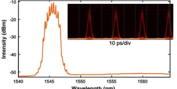
At the output of the GeAsSe fiber, a 2 nm filter is used to extract the idler wave centered at 1545.4 nm. The power of the idler wave is measured to be −18.5 dBm. It is then amplified by an EDFA and then re-filtered by a 1 nm Gaussian filter to reshape the signal. The pulse duration of the demultiplexed signal is measured to be 3.9 ps. Fig. 4 shows an example of the spectrum of one demultiplexed 42.7 Gb/s tributary channel and its corresponding eye diagram.
10 ps/div 10 ps/div Wavelength (nm) In te n s it y (d B m ) 1540 1545 1550 1555 1560 -50 -40 -30 -20 -10 1540 1545 1550 1555 1560 -50 -40 -30 -20 -10
Fig. 4 Spectrum of the 42.7 Gb/s demultiplexing signal. The inset is the corresponding eye-diagram.
To assess the performance of our FWM-based all-optical demultiplexer, the bit-error-rate (BER) has been measured for the 4 demultiplexed channels. Fig. 5 represents the BER evolution as a function of the received power for the best channel and the worst channel. The back-to-back (B2B) cases at 42.7 Gb/s and 170.8 Gb/s are also represented. We observe a maximum power penalty of 3.5 dB with respect to the 42.7 Gb/s B2B. The power penalty can be attributed to dispersion and nonlinear effects. Indeed chromatic dispersion introduces a walk-off delay of about 500 fs between the data signal and the clock signal after 30 cm of propagation. This can cause noise fluctuations on the demultiplexed signal. Spectral broadening of the 42.7 GHz clock due to SPM can also cause optical signal-to-noise degradation of the demultiplexed signal. 1.0E-10 1.0E-09 1.0E-08 1.0E-07 1.0E-06 1.0E-05 1.0E-04 -35 -33 -31 -29 -27 -25 Received power (dBm) B E R 170 Gb/s B2B 42.7 Gb/s B2B
42.7 Gb/s Demux - best case 42.7 Gb/s Demux - worse case
Fig. 5 BER evolution of the demultiplexed signal and B2B.
Conclusion: We have presented a chalcogenide GeAsSe
microstructured fiber with a high nonlinear coefficient and low losses. All-optical time-domain demultiplexing of a 170.8 Gb/s signal down to 42.7 Gb/s has been experimentally demonstrated with a total average power of only 56 mW. These results show the capability of
chalcogenide microstructured fibers to perform all-optical signal processing at high bit rate.
Acknowledgments: This work is supported by the Conseil Régional de
Bretagne, the Conseil Général des Côtes d’Armor, the European Union Feder program and the French government.
S. D. Le, M. Gay, L. Bramerie, T. Chartier, M. Thual, J.-C. Simon (CNRS Foton (UMR 6082), 6 rue de Kerampont, BP 80518, 22305
Lannion cedex, France)
E-mail: sy-dat.le@enssat.fr
L. Brilland, D. Méchin (PERFOS, R&D platform of Photonics
Bretagne, 11 rue Louis de Broglie, 22300 Lannion, France)
P. Toupin, J. Troles (CNRS Institut des Sciences Chimiques de Rennes
(UMR 6226), Université de Rennes 1, 35000 Rennes, France)
S. D. Le, M. Gay, L. Bramerie, T. Chartier, M. Thual, J.-C. Simon, P. Toupin, J. Troles are also with Université européenne de Bretagne, 5
Boulevard Laënnec, 35000 Rennes, France References
1 B. Olsson and D. Blumenthal, “All-optical demultiplexing using fiber cross-phase modulation (XPM) and optical filtering,” IEEE Photon.
Technol. Lett., 2001, 13, p. 875.
2 T. Vo, H. Hu, M. Galili, E. Palushani, J. Xu, L. Oxenløwe, S. Madden, D. Choi, D. Bulla, M. Pelusi et al., “Photonic chip based transmitter optimization and receiver demultiplexing of a 1.28 tbit/s OTDM signal,” Opt. Express, 2010, 18, p. 17252.
3 F. Li, M. Pelusi, D-X. Xu, A. Densmore, R. Ma, S. Janz, and D.J. Moss, “Error-free all-optical demultiplexing at 160 Gb/s via FWM in a silicon nanowire,” Opt. Express, 2010, 18, p. 3905.
4 T. Yamamoto, E. Yoshida, and M. Nakazawa, “Ultrafast nonlinear optical loop mirror for demultiplexing 640 Gbit/s TDM signals,”
Electron. Lett., 1998, 34, p. 1013.
5 S. D. Le, D. Nguyen, M. Thual, L. Bramerie, M.C. e Silva, K. Lengle, M. Gay, T. Chartier, L. Brilland, D. Mechin, P. Toupin, and J. Troles, “Efficient four-wave mixing in an ultra-highly nonlinear suspended-core chalcogenide As38Se62 fiber,” Opt. Express, 2011, 19, p. B653.
6 P. Toupin, L. Brilland, J. Troles, and J.-L. Adam, “Small core GeAsSe microstructured optical fiber with single-mode propagation and low optical losses,” Opt. Mater. Express, 2012, 2, p. 1359.