HAL Id: hal-01226769
https://hal.archives-ouvertes.fr/hal-01226769
Submitted on 10 Nov 2015
HAL is a multi-disciplinary open access
archive for the deposit and dissemination of
sci-entific research documents, whether they are
pub-lished or not. The documents may come from
teaching and research institutions in France or
abroad, or from public or private research centers.
L’archive ouverte pluridisciplinaire HAL, est
destinée au dépôt et à la diffusion de documents
scientifiques de niveau recherche, publiés ou non,
émanant des établissements d’enseignement et de
recherche français ou étrangers, des laboratoires
publics ou privés.
A Thresholder for All-Optical Digitising
Radio-over-Fibre Transceivers
Ricardo Ribeiro, Frédéric Lucarz, Bruno Fracasso
To cite this version:
Ricardo Ribeiro, Frédéric Lucarz, Bruno Fracasso. A Thresholder for All-Optical Digitising
Radio-over-Fibre Transceivers. OMDM 2013 : 17th international conference on Optical Network Design and
Modeling, Apr 2013, Brest, France. pp.161 - 166. �hal-01226769�
1 2 3 4 5 6 7 8 9 10 11 12 13 14 15 16 17 18 19 20 21 22 23 24 25 26 27 28 29 30 31 32 33 34 35 36 37 38 39 40 41 42 43 44 45 46 47 48 49 50 51 52 53 54 55 56 57 60 1
Abstract—This paper describes an optical Thresholder
(o-Thresholder) intended to be part of a transmitter module for
future all-optical Digitising Radio-over-Fibre (o-DRoF) transceivers. The proposed device is based on an
Attenuation-Imbalanced Semiconductor Laser Amplifier Loop Mirror
(AI-SLALOM) in self-switching regime, using the nonlinearities of a semiconductor optical amplifier. Simulations of the proposed AI-SLALOM based o-Thresholder have shown promising results in comparison with the use of standard optical fibre and highly nonlinear fibre only. The newly proposed device is rather compact, optically integrable and requires much less input optical power than conventional devices (by several orders of magnitude). It provides enhanced optical RZ bits at 1550 nm wavelength window, 1.25 GHz repetition rate and 80 ps time-width.
Index Terms—Analogue-digital conversion, Microwave Photonics, Optical Signal Processing, Semiconductor optical amplifiers.
I. INTRODUCTION
NALOGUE Radio-over-Fibre (ARoF) is a key-technology for the convergence of fibre-based wireline and wireless networks [1] and by means of which a large variety of mobile and wireless services including UMTS, LTE, Wi-Fi and WiMAX may be seamlessly delivered to customers. Merging RoF and FTTx (Fibre-To-The-x) technologies, namely FTTA (A = Antenna), is a promising approach to provide reliable mobile and wireless broadband access with a higher level of densification and enhanced network capacity. ARoF allows a relatively simple distribution of RF signals over an optical carrier along optical fibres connecting a Central Station (CS) to Base Stations (BSs) or Remote Antenna Units (RAUs). Therefore, all signal processing may be centrally carried out at the CS [1,2], leading to simple RAUs design that only needs to implement optoelectronic conversion and power amplification.
Ricardo M. Ribeiro is permanently with the Laboratório de Comunicações Ópticas, Departamento de Engenharia de Telecomunicações, Universidade Federal Fluminense, 24.210-240, Niterói, RJ, Brasil (phone: +55-21-2629-5602; fax: +55-21-2629-5521) and thanks Foundation Capes/MEC-Brasil for the financial support through a Post-Doctoral fellowship under the grant BEX 9096/11-6.
Ricardo M. Ribeiro, Frédéric Lucarz and Bruno Fracasso are with the Département d’Optique, Telecom Bretagne, Technopôle Brest-Iroise, CS 83818, 29238, Brest, Cedex 3, France (e-mails: [email protected],
[email protected], [email protected]).
However, ARoF systems are constrained by two basic requirements, which are inherent to analogue transmissions [1]: all used devices should be highly linear and the received signal should have higher SNR (Signal to Noise Ratio) when compared with digital systems. Since ARoF networks require high SNRs, their analogue nature limits the accepted fibre attenuation and the splitting ratio of optical signals, both critical in FTTH (H = Home) networks. Furthermore, the accelerated deployment of wireless networks operating at increased carrier frequencies up to ~ 100 GHz, leads to networks with naturally reduced coverage area per antenna.
In order to circumvent the limitations of ARoF networks, the use of digitised radio-over-fibre (DRoF) technologies [2,3] is an interesting alternative. In electronic DRoF links, the analogue RF input signal is first digitised by an analogue-to-digital converter (ADC). The generated electrical bits drive a light source thus generating optical bits then transported over optical fibre and finally reconstructed by a digital-to-analogue converter (DAC) at the output of a photo-detector. Each BS (or RAU) comprises one ADC and one DAC, while more complex digital signal processing is carried out in the CS [2]. Due to the digital nature of the optical link, the dynamic range is independent of the fibre length as long as the power of the received signal is lower than the link sensitivity. Electronic DRoF technologies still exhibit some advantages of ARoF [2,3] except for its relative higher complexity, but include further characteristics as follows: centralized digital signal processing such as digitisation itself, enhanced sharing capacity and better compatibility of digital equipments and communication channels, significant increase in transmission distance using optical fibre (larger dynamic range), larger coverage capacity or larger number of RAUs, possible cost reduction and energy saving.
The all-photonic signal conversion and processing are required due to the accelerated growth of demanded traffic reaching Exabyte per month. Therefore, high-speed processing and transmission are essential. Next-generation networks will face congestion in the backbone, metropolitan and access networks. Congestion in the backbone is due to the bottleneck of 3R processing (re-timing, re-shaping and re-amplifying) in the electronic domain. All these processes require optical/electrical (O/E) conversion that introduces complexities and delays. The switching and routing electronic process of the traffic in the backbone and metropolitan networks may also cause congestion. The use of all-optical switching and routing devices together with proper protocols
A Thresholder for All-Optical Digitising
Radio-over-Fibre Transceivers
Ricardo M. Ribeiro, Frédéric Lucarz and Bruno Fracasso
1 2 3 4 5 6 7 8 9 10 11 12 13 14 15 16 17 18 19 20 21 22 23 24 25 26 27 28 29 30 31 32 33 34 35 36 37 38 39 40 41 42 43 44 45 46 47 48 49 50 51 52 53 54 55 56 57 60 61 2 can significantly mitigate this problem. Therefore, by using
all-photonic DRoF more operations and signal processing centralisation at the CS could be achieved. The main challenges in the electronic DRoF link implementation are: high-speed ADC and DAC, dispersions, nonlinearities (in the electrical and optical domains), additive noise, integration of system and devices, size and system cost.
An o-DRoF transmitter comprises an RF interface, an all-optical ADC and an enhancer/amplifier to significantly increase the optical-bit contrast. To the best of our knowledge, no complete experimental all-optical DRoF communication system has been reported in the literature. However, some recently published papers [3-6] from Brunel University (UK) report valuable theoretical simulations of an o-DRoF system but without any detailed description of the operational principles of both all-optical ADC and DAC.
In the present paper, the use of an AI-SLALOM configuration is proposed as a self-switched o-Thresholder circuit to be part of a future o-DRoF transceiver. Simulation results on VPI Transmission Maker TM and comparisons of the proposed AI-SLALOM and Attenuation Imbalanced Nonlinear Optical Loop Mirrors (AI-NOLMs) using standard (SF) and highly nonlinear optical fibres (HNLFs)
o-Thresholder configurations are presented for 1550 nm
wavelength window, 1.25 GHz repetition rate with 80-ps RZ pulses. Because the proposed o-Thresholder uses a laser
amplifier as the nonlinear optical element, their optical circuit may potentially perform additional signal processing, such as wavelength conversion and modulation format conversion [7,8]. The o-DRoF systems may well integrate the next generation of all-photonic telecommunication networks [3-6] and provide the connection between the access and metropolitan or even transport networks.
II. ALL-OPTICAL DIGITISING RADIO-OVER-FIBRE (O-DROF) TRANSMITTER
This section proposes an o-DRoF transmitter able to receive and process ARoF signals that essentially comprises a photonic-ADC and a photonic-thresholder.
Electronic ADC and DAC boards seem to exhibit an intrinsic limitation in their stability, “bit resolution x input frequency” product and data conversion rates of up to a few tenths of GSa/s [3-6,9]. Besides, the vast majority of all-optical ADC and DAC systems have always been separately reported and for various types of applications, but excluding any communication link application.
Figure 1 depicts a typical and simplified transmitter module flowchart of an o-DRoF link [9,10].
Fig. 1. The simplified flowchart of a complete o-DRoF transmitter. The o-Thresholder sub-module treated in this paper is numbered as (5). The o-DRoF transmitter comprises at least five main optical
sub-modules: (1) optical pulse generator (o-Generator), (2) optical sampler (o-Sampler), (3’and 3’’) temporal interleavers (o-Interleaver), (4) encoder (o-Encoder) and (5) thresholder (o-Thresholder). The o-Sampler carries out the optical sampling of an input ARoF signal. It is driven by an optical pulse comb that is generated by the o-Generator. This pulse
comb is also used as a reference clock signal by the o-Encoder that optically encodes the sampled signal, thereby accomplishing the photonic AD-conversion itself.
The o-Thresholder is provided mainly to enhance the contrast between the “0” and “1” optical bits at the output of the o-Encoder.
The o-Generator is preferably implemented by a mode-locked laser, a key component used to generate a series of
1 2 3 4 5 6 7 8 9 10 11 12 13 14 15 16 17 18 19 20 21 22 23 24 25 26 27 28 29 30 31 32 33 34 35 36 37 38 39 40 41 42 43 44 45 46 47 48 49 50 51 52 53 54 55 56 57 60
picosecond pulses at GHz rates with high temporal stability, i.e. with very low jitter in the femtosecond time-scale [9,10] so that these pulses can be used as the clock signal for the optical sampling and coding. The o-Interleavers essentially multiply the repetition rate of the clock signal generated by the
o-Generator.
III. MODELLING AND SIMULATIONS OF THE O-THRESHOLDER Sagnac interferometric fibre rings have been used as a nonlinear device based on self-phase modulation (SPM) or cross-phase modulation (XPM) – NOLMs – that are very useful for many ultrafast signal-processing applications [11]. The use of a laser amplifier as a nonlinear medium instead of the optical fibre leads to an interesting class of devices usually named as SLALOM [12] or Terahertz Optical Asymmetric Demultiplexer (TOAD) [13].
Three different optical circuits of the o-Thresholder were designed and simulated using VPI Transmission MakerTM. All circuits were probed at 1550 nm wavelength window with 1.25 GHz repetition rate, 80 ps time-width RZ pulse stream. The peak power of the input pulses (Pinput) could be varied from 10 µW to 10 W in order to obtain the transfer functions – the Poutput /Pinput curves – for the three optical circuits.
The input pulses at 1553.6 nm wavelength were generated from a continuous-wave laser diode with null linewidth after traversing a Mach-Zehnder modulator (MZM). The MZM is biased at the quadrature point and is driven by 2.5 Gb/s RZ electrical pulses in an alternate pattern with 0.1 duty-cycle.
The optical circuits are attenuation-imbalanced Sagnac interferometers instead of using fibre-couplers with coupled-ratio ≠ 50:50 thus allowing a maximum interference visibility contrast. The insertion of an attenuator (passive component) in the Sagnac fibre ring provides the necessary differential phase-shift between the clockwise (CW) and counter-clockwise pulses (CCW). The polarisations of the CW and CCW pulses are assumed to be always aligned. Such a condition can be achieved in practice by using polarisation controllers in the optical circuits or by using polarisation-maintaining fibres.
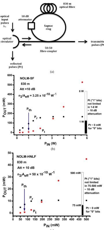
Figure 2a depicts a first design of the o-Thresholder with an optical circuit using a NOLM with standard fibre. Table I shows the optical fibre parameters as used in the simulations. The Aeff is the effective area of the fibre. The physical model solves the nonlinear Schrödinger equation (NLSE) taking into account the SPM and XPM in the single-mode fibre [14].
The 10 dB attenuator breaks the reciprocity of the Sagnac ring thus CW and CCW pulses accumulate a Δφ differential phase-shift. Therefore, the Δφ parameter determines the relative amount of reflected (Pr) and transmitted (Pt) power.
(a)
(b)
(c)
Fig. 2. (a) The optical circuit of the o-Thresholder based on NOLM-SF (according to the first design) or NOLM-HNLF (according to the second design), (b) the transfer function of the NOLM-SF and the (c) NOLM-HNLF
1 2 3 4 5 6 7 8 9 10 11 12 13 14 15 16 17 18 19 20 21 22 23 24 25 26 27 28 29 30 31 32 33 34 35 36 37 38 39 40 41 42 43 44 45 46 47 48 49 50 51 52 53 54 55 56 57 60 61 4
Figure 2b shows the result of the transfer function simulations according to the first design (see Figure 2a). All pulses up to ~1 W peak power are reflected, i.e. the “0” bits with almost zero power are transmitted. A least from 1 W to 6 W input, the power of the transmitted “1” bits are not really limited. As expected, despite the PIN input power, the Pr + Pt power sum is 10 dB attenuated. For this first design the threshold power Pth of the AI-NOLM-SF may be set at 1 W.
According to a second design, the topology of the NOLM-HNLF optical circuit was exactly the same as shown in Figure 2a, with the exception that now the fibre is Dispersion-Shifted Fibre (DSF) [9]. Table I shows the optical fibre parameters as used in the simulations where the optical nonlinearity of the HNLF is 50/3.25 ~15 times higher than that of the SF. Figure 2c shows the result of the simulations obtained with the
second design. All pulses up to 75 mW peak power are
reflected, i.e. the “0” bits with almost zero power are transmitted. A least from 75 to 500 mW input peak power, the output power of the transmitted “1” bits are not really limited. As again expected, despite the PIN input power, the Pr + Pt power sum is 10 dB attenuated. For this second design the threshold power of the AI-NOLM-HNLF may be set at Pth = 75 mW. In these first two designs, the switching mechanism is driven by the SPM effect occurring into the optical fibre [11,14].
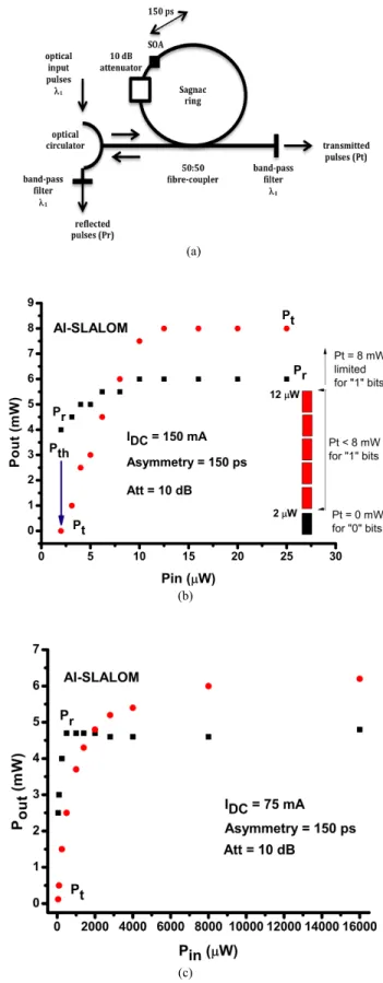
Figure 3a depicts a third design of the o-Thresholder based now on an AI-SLALOM optical circuit using a SOA as the nonlinear optical element instead of an optical fibre. The physical model takes into account a bulk SOA with low feedback neglecting the polarisation effects (isotropic model) and uses the Transmission Line Model (TLM) to compute the differential nonlinear phase-shift induced by a change in carrier density in the semiconductor. In this way, the switching
is again driven by the SPM effect now occurring into the SOA. Table I shows the SOA parameters as used in the computer simulations.
(a)
(b)
1 2 3 4 5 6 7 8 9 10 11 12 13 14 15 16 17 18 19 20 21 22 23 24 25 26 27 28 29 30 31 32 33 34 35 36 37 38 39 40 41 42 43 44 45 46 47 48 49 50 51 52 53 54 55 56 57 60 (d)
Fig. 3. (a) The optical circuit of the AI-SLALOM based o-Thresholder (according to the third design), the transfer function as a result from simulations (b) with IDC = 150 mA and (c) IDC = 75 mA bias current, and the
zoom of the transfer function at low input power (from Fig. (c)). The asymmetric placement of the SOA at 150 ps from the mid-point of the fibre ring ensures that the gain is completely recovered for either the CW or CCW pulses. This limits the speed of the device as explained in the “Conclusions”. The optical circulator allows the separation between the input and reflected pulses. The band-pass filters reduce the Amplified Spontaneous Emission (ASE) generated by the SOA and detected by the analysers. The centre frequency and spectral width of the filters are set to be 1553.6 nm and 100 GHz (0.8 nm), respectively.
Figure 3b shows the simulation results obtained for the
third design (see Figure 3a) with a bias current set to IDC = 150 mA. All pulses with a peak power of up to 2 µW are reflected, i.e. the “0” bits with almost zero power are transmitted. In the 2-10 µW range is observed a fast transition from ~ 0 to 8 mW output power. For input optical pulses with a peak power greater than 10 µW, the output power of the transmitted “1” bits are now limited at 8 mW. Therefore, the transmitted (and also the reflected) pulses are now optically amplified/limited. For this third design with IDC = 150 mA, the threshold power may be set at Pth = 2 µW.
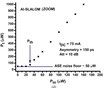
Figure 3c shows the simulation results obtained for the third
design (see Figure 3a) with a bias current set to IDC = 75 mA. Figure 3d is the zoom of Figure 3c at low input powers. All pulses with peak power of up to Pth = 30 µW are essentially reflected because only noisy signals are calculated, even for Pin = 0 µW. This may be due to ASE noise combined with numerical artefacts. Therefore, the “0” bits with almost zero power are transmitted. In the 30 µW - 6 mW input power range is observed a non-abrupt transition presenting output gain. For input optical pulses with a peak power greater than 8 mW, the output power of the transmitted “1” bits are now limited at 6 mW (negative gain). Therefore, the transmitted (and also the reflected) pulses are optically amplified and/or limited. For this third design with IDC = 75 mA, the threshold power may be set at Pth = 30 µW. As expected, the amplifier gain is reduced because the bias current is also reduced.
However, the ASE power level is also significantly reduced. It is also shown that it is possible to easily tune the threshold power of the o-Thresholder from 2 µW to 30 µW.
Comparing the three designs of o-Thresholders, the use of HNLF instead of SF requires over 11 dB less input power. The use of SOA instead of HNLF requires less than 30 dB input power to obtain the switching. Furthermore, the SOA is only 1-mm long while the HNLF is 830 m in length. The results with SOA are in agreement with a similar work [15]. For fibre lengths greater than a few hundred meters, the stability of the NOLM is significantly degraded. Furthermore, the long fibre introduces excessive latency for some optical processing applications [16]. By comparing the active length and threshold power between the AI-SLALOM and the AI-HNLF configurations, i.e. by setting (Δφ)AI-SLALOM = (Δφ)AI-HNLF, it is easy to estimate an optical nonlinearity (n2) of ~ 5 x 10¹⁰ times greater when a semiconductor laser amplifier is used as a nonlinear optical element instead of a DSF-fibre. D. Cotter et
al have described the implementation of a SLALOM circuit on
a single 1x2 mm InP semiconductor chip [16] that demonstrates the possibility of optical integration of the proposed o-DRoF transmitter.
Figure 4 shows an example of application of the AI-SLALOM based o-Thresholder with the SOA set at IDC = 75 mA bias current, useful for an o-DRoF transmitter.
Fig. 4. An example of application of the 1-stage AI-SLALOM based o-Thresholder that is useful for an o-DRoF transmitter.
After the simulation of Figure 3c and 3d using an AI-SLALOM biased at IDC = 75 mA, the threshold power of 30 µW at 50 % (or the corresponding threshold voltage level) may be a conservative choice for the decision circuit of a digital receiver. The example of Figure 4 shows a “00010101010” poor quality input bits sequence assumed to be generated by the Encoder. After traversing 1-stage
1 2 3 4 5 6 7 8 9 10 11 12 13 14 15 16 17 18 19 20 21 22 23 24 25 26 27 28 29 30 31 32 33 34 35 36 37 38 39 40 41 42 43 44 45 46 47 48 49 50 51 52 53 54 55 56 57 60 61 6
Thresholder, the output optical bits are fairly enhanced, i.e. the
“0” bits present 50 µW maximum output power whereas the “1” bits are all amplified to reach (175 ± 25) µW peak power. Using 4-stage o-Thresholders with alternated 3-dB attenuators, it is now possible to achieve “0” bits presenting 50 µW maximum output power whereas the “1” bits are all amplified to reach (3.1 ± 0.1) mW peak power, i.e. a highly improved limitation. Of course, a better design of the
o-Thresholder shall enable the use of 1 or 2 circuit stages only.
Alternatively, the transmission port of a first AI-SLALOM biased at IDC = 75 mA may be followed by an ~17 dB optical attenuator in turn connected to the input port of a second AI-SLALOM biased at IDC = 150 mA (or 75 mA < IDC < 150 mA) presenting a threshold power of 2 µW or (2 µW Pth < 30 µW) (or the corresponding threshold voltage level). The previous optical circuit comprising 2-stage AI-SLALOMs allows that the transmission output could be almost perfect “0” bits (null optical power) and “1” bits with 1.0 – 2.5 mW optical power.
IV. CONCLUSIONS
To the best of our knowledge, neither experimental nor commercially available o-DRoF links or networks have been reported as they are still under R&D stage. This paper proposes a system comprising five optical sub-modules for use in an o-DRoF transmitter link. The present paper only described the back-end sub-module of the o-DRoF transmitter, i.e. the AI-SLALOM based o-Thresholder in a self-controlled (or self-switched) regime operating at 1550 nm wavelength window. The proposed AI-SLALOM configuration when compared with the AI-HNLF [9] may provide some advantages: compactness, prone to optical integration, requirement of ~103 less optical power and automatically amplified output optical bits. Mainly to demonstrate the
proof-of-principle, in this paper the simulations were constrained to
only 1.25 GHz & 80-ps RZ input pulses. However, SOAs operating at 80 Gb/s are already commercially available. Furthermore, SOAs in R&D stage able to operate up to 160 Gb/s [17] and beyond were already reported. The newly proposed o-Thresholder is intended to significantly enhance the contrast of digitised signals (optical bits) exiting an
o-Encoder thus improving the Bit-Error Rate (BER) and also
providing optical amplification eventually dispensing the use of Erbium-Doped Fibre Amplifier (EDFAs) in a fibre link transmission.
Further simulations (and laboratory experiments) of the
o-Thresholder and the other sub-modules of the o-DRoF
transmitter are currently planned or in progress and will be presented in a near future. Examples of scheduled device simulation improvements to be carried out include: operation at higher pulse rate (> 1.25 GHz) with shorter timewidth (< 80-ps), smaller asymmetry (< 150 ps) of the SOA placement in the Sagnac fibre ring in order to speed the operation [12], to tune the threshold power and to obtain a steeper transition region, etc.
ACKNOWLEDGMENT
Ricardo M. Ribeiro would like to thank the team at Département d’Optique of Telecom Bretagne and the CapilRTM platform for hosting his Post-Doctoral study during which the present work was carried out.
REFERENCES
[1] R. C. Williamson and R. D. Esman, RF Photonics, Journal of Lightwave Technology, Vol. 26, No. 9, 2008, pp. 1145-1151.
[2] A. Nirmalathas et al, Digitized Radio-Over-Fiber Technologies for Converged Optical Wireless Access Network, IEEE Journal of Lightwave Technology, Vol. 28, No. 16, 2010, pp. 2366 –2375. [3] S. R. Abdollahi, H. S. Al-Raweshidy and R. Nilavalan, Fully-Photonic
Analogue-to-Digital Conversion Technique for Super-Broadband Digitized-Radio over Fibre Link, 16th European Conference on Networks and Optical Communications, Newcastle, UK, 20-22 July, 2011, pp. 72-75.
[4] S. R. Abdollahi et al, Digital Radio over Fibre for Future Broadband Wireless Access Network Solution, 6th International Conference on Wireless and Mobile Communication, Valencia, Spain, September, 20-25, 2010.
[5] S. R. Abdollahi et al, Non-Uniform Wavelength Allocation in All-Photonic Digitized-Radio over Fibre Access Network, 14th International Symposium on Wireless Personal Multimedia Communications, Brest, France, October, 2011.
[6] A. Viglienzoni and H. Al-Raweshidy, Net! Works - Next Generation Network: Wireless-Optics Technology, European Technology Platform, White Paper, 2011, June 06.
[7] I. D. Phillips et al, Simultaneous demultiplexing, data regeneration, and clock recovery with a single semiconductor optical amplifier-based nonlinear-optical loop mirror, Optics Letters, Vol. 22, No. 17, 1997, pp. 1326-1328.
[8] X. Yang et al, Application of Semiconductor Optical Amplifiers in High-Speed All-Optical NRZ to RZ Format Conversion, ICTON 2007, Paper We.D2.3, 2007, pp. 228-231.
[9] Y. Miyoshi et al, All-Optical Analog-to-Digital Conversion Using Split-and-Delay Technique, Journal of Lightwave Technology, Vol. 25, No. 6, 2007, pp. 1339-1347.
[10] M. Currie, High-Performance Photonic Analog-to-Digital Converter and Low-Noise Mode-Locked Fiber Laser, U.S. Navy, Final Report, NRL/MR/5650--03-8679, 2003, May 26.
[11] G. Huang et al, All-Optical OOK to 16-QAM Modulation Format Conversion Employing Nonlinear Optical Loop Mirror, Journal of Lightwave Technology, Vol. 30, No. 9, 2012, 1342-1350.
[12] M. Eiselt, Optical Loop Mirror with Semiconductor Laser Amplifier, Electronics Letters, Vol. 28, No. 16, 1992, pp. 1505-1507.
[13] J. P. Sokoloff et al, A Terahertz Optical Asymmetric Demultiplexer (TOAD), IEEE Photonics Technology Letters, Vol. 5, No. 7, 1993, pp. 787-790.
[14] G. P. Agrawal, Self-Phase Modulation in Optical Fiber Communications: Good or Bad?, CLEO 2007, paper JTuB5, 2007, May 6-11.
[15] A. W. O’Neill and R. P. Webb, All-Optical Loop Mirror Switch Employing an Asymmetric Amplifier/Attenuator Combination, Electronics Letters, Vol. 26, No. 24, 1990, pp. 2008-2009.
[16] D. Cotter et al, Nonlinear Optics for High-Speed Digital Information Processing, Science, Vol. 286, 1999, pp. 1523-1528.
[17] K. Szuki et al, Error-free demultiplexing of 160 Gbit/s pulse signal using optical loop mirror including semiconductor laser amplifier, Electronics Letters, Vol. 30, No. 18, 1994, pp. 1501-1503.
![Figure 1 depicts a typical and simplified transmitter module flowchart of an o-DRoF link [9,10]](https://thumb-eu.123doks.com/thumbv2/123doknet/11654067.308901/3.918.270.674.541.910/figure-depicts-typical-simplified-transmitter-module-flowchart-drof.webp)