HAL Id: hal-03175704
https://hal.archives-ouvertes.fr/hal-03175704
Submitted on 20 Mar 2021
HAL is a multi-disciplinary open access
archive for the deposit and dissemination of
sci-entific research documents, whether they are
pub-lished or not. The documents may come from
teaching and research institutions in France or
abroad, or from public or private research centers.
L’archive ouverte pluridisciplinaire HAL, est
destinée au dépôt et à la diffusion de documents
scientifiques de niveau recherche, publiés ou non,
émanant des établissements d’enseignement et de
recherche français ou étrangers, des laboratoires
publics ou privés.
toward new micro-architectural fault models
Thomas Trouchkine, Sébanjila Kevin Bukasa, Mathieu Escouteloup, Ronan
Lashermes, Guillaume Bouffard
To cite this version:
Thomas Trouchkine, Sébanjila Kevin Bukasa, Mathieu Escouteloup, Ronan Lashermes, Guillaume
Bouffard. Electromagnetic fault injection against a complex CPU, toward new micro-architectural
fault models. Journal of Cryptographic Engineering, Springer, 2021, �10.1007/s13389-021-00259-6�.
�hal-03175704�
(will be inserted by the editor)
Electromagnetic fault injection against a complex CPU,
toward new micro-architectural fault models
Thomas Trouchkine · Sébanjila Kevin Bukasa · Mathieu Escouteloup · Ronan Lashermes · Guillaume Bouffard
Received: date / Accepted: date
Abstract The last years have seen the emergence of fault attacks targeting modern central processing units (CPUs). These attacks are analyzed at a very high abstraction level and, due to the modern CPUs com-plexity, the underlying fault effect is usually unknown. Recently, a few articles have focused on characterizing faults on modern CPUs.
In this article, we focus on the electromagnetic fault injection (EMFI) characterization on a bare-metal im-plementation. With this approach, we discover and un-derstand new effects on micro-architectural subsystems. We target the BCM2837 where we successfully demon-strate persistent faults on L1 instruction cache, L1 data cache and L2 cache. We also show that faults can cor-rupt the memory management unit (MMU). To validate our fault model, we realize a persistent fault analysis to retrieve an AES key.
Keywords Physical attacks · Fault models · Electro-magnetic Fault Injection (EMFI) · System-on-Chip (SoC)
S. K. Bukasa· M. Escouteloup INRIA/CIDRE, Rennes, France R. Lashermes
INRIA/SED, Rennes, France T. Trouchkine· G. Bouffard
National Cybersecurity Agency of France (ANSSI) 51, boulevard de La Tour-Maubourg
75700 Paris 07 SP, France
E-mail: [email protected] G. Bouffard
DIENS, École normale supérieure, CNRS, PSL University, Paris, France E-mail: [email protected]
1 Introduction
Sensitive operations are usually performed on secure-oriented devices such as smartcards. These kinds of vices are hardened microcontroller units (MCUs) de-signed to be tamper resistant against hardware and software attacks. They are evaluated under a scheme, e.g. Common Criteria, to ensure a high security level. Smartcards are the most studied secure-oriented de-vices.
Recently, sensitive operations are increasingly per-formed on more powerful and complex devices: the system-on-chips (SoCs). These SoCs are powered by central processing units (CPUs) with a complex micro-architec-ture including memory virtualization, several cache lev-els, speculative or out-of-order execution.
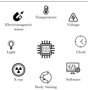
To behave correctly, components have to fulfill phys-ical constraints. These constraints are directly linked to their design and, if they are respected in their nominal operation point, it is possible to break these constraints conditions by inducing stimuli in the component as pre-sented in Figure 1.
When a stimuli perturbs the component, it is pushed to its operation limit. Therefore, faults can be induced. Among all the fault injection methods, electromag-netic fault injection (EMFI) has been demonstrated to be effective on the complex CPUs with a minimal effort on target preparation [8] and without chip alteration.
Complex CPUs are tuned for the best performance/en-ergy consumption trade-off and are focused on software hardening. However, hardware security is not the main
Clock Voltage Temperature Electromagnetic waves Light X-ray Body biasing Software
Fig. 1: Stimuli able to perturb a component
concern and past works [8, 11, 12, 18, 19, 20, 25] have shown that physical attacks are effective against them. These articles demonstrate the need for hardening complex CPUs against fault attacks. To achieve that goal, we first need to understand the effects of such faults on the micro-architecture.
To model the fault effects, literature [1, 2, 10, 13, 15, 26, 28] covers mostly a simple component: the MCU. The MCU is cheaper and smaller than a complex CPU without advanced micro-architectural components. Their works improve the hardware security of MCU and a lot of introduced countermeasures are embedded in smart-cards. However, the obtained fault model cannot be scaled up on complex CPUs embedded in SoCs due to the latter’s hardware complexity.
Some recent papers [14, 21] have proposed fault characterizations on complex CPUs. However, since they use a device running a complex operating system (OS), their analysis cannot precisely infer the impact on micro-architectural elements.
In this work, we propose instead to run our open-source characterization software1as a bare-metal
appli-cation for the Raspberry Pi 3 B (RPi3)’s CPU embed-ded in the BCM2837 SoC. This implementation allows us to have control of software/hardware interactions. Therefore, we can realize a finer grained characteri-zation on several micro-architectural components. To fault the BCM2837 CPU, we first make EMFI and we next use a forensic process based on JTAG debug port
1 This implementation and the experiment data are released
as open-source software (MIT License) here: https://gitlab. inria.fr/rlasherm/rpi3_fault_analysis.
to understand fault effects.
In this article, we highlight several new fault ef-fects at the micro-architectural level, in particular in the memory hierarchy.
This article is organized as follows. The BCM2837 is described in section 2. On its complex CPU, we run a nested for loop and we vary the injection delay. The experimentation modus operandi is explained in sec-tion 3.
Regarding this experimentation, we observed faults on different micro-architecture blocks:
– on the L1 instruction cache where we achieve a per-sistent fault in the L1 instruction cache as described in section 4,
– on the memory management unit (MMU); we con-fuse the virtual-to physical memory mapping. This fault is introduced in section 5,
– on the L2 cache; we also achieve a persistent fault in the L2 cache demonstrated in section 6.
A fault exploitation demonstration is given in sec-tion 7 with a persistent fault in the L1 data cache, where an AES cryptographic key is recovered with one fault injection and 224
hypotheses.
We finish with propositions to protect complex CPUs against these attacks in section 8. Section 9 puts our work in the state of the art and we conclude in sec-tion 10.
2 BCM2837 description
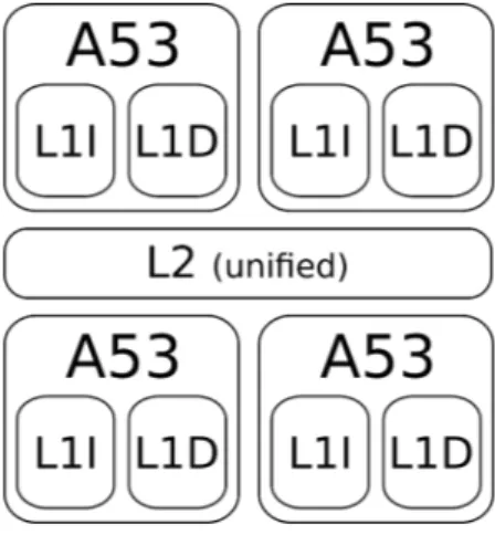
The RPi3 is a low-cost single-board computer. It fea-tures a complete system able to run a complex OS such as Linux or Windows and their applications. The SoC powering this board is the BCM2837 from Broadcom, a 28 nm quad-core Cortex-A53 CPU running at 1.2 GHz with the help of a dual-core VideoCore IV GPU at 400 MHz. This SoC also features 512 kB of cache mem-ory and various wireless or contact connections such as HDMI, Wi-Fi, ethernet, USB, etc.
Our experiments are performed with our own soft-ware stack, with only one core active. Indeed, even if we tested EMFI with several cores enabled, it is hard to pinpoint the exact effect on the micro-architecture in this configuration since we cannot easily link a fault in unified memory with a particular core. Therefore, to in-crease our confidence in our characterization, we enable only one core.
To control the chip’s behavior, we have implemented the minimum to run our applications: initialization of
JTAG, UART, GPIO, CPU caches and MMU. We want to stress out that no complex OS is running during our experiments in sections 4, 5, 6 and 7, to avoid interfer-ence that could hinder our ability to infer more precise fault models. In particular, we try to avoid the context switching effects due to preemptive scheduling by the OS, the error recovery mechanisms (if an error occurs, we want to know it) and the cache maintenance per-formed by the OS.
In order to later explain the causes of the failures observed, we describe in more details two important micro-architecture blocks of this complex CPU: the cache hierarchy and the MMU.
2.1 Cache hierarchy
In modern systems, memory accesses are a lot slower than the arithmetic logic unit (ALU). To avoid losing too much performance to this latency difference, small and fast memories called caches are used to mirror a part of the memory space.
First, in the targeted CPU, each core has two L1 caches (the smallest and fastest kind), one dedicated to instructions (L1I), one to data (L1D). These caches are 16 kB in size with 64 B line width.
Second, the second layer of cache memory, the L2 cache, is common to all cores and thus provides a unified view of the memory space. Its size is 512 kB with 64 B line width.
The cache organization is displayed in Figure 2. The bus sizes between memory elements are given in Table 1
Fig. 2: BCM2837 memory hierarchy.
Source Destination Bus size (bits)
RAM L2 128 L2 L1I 128 L2 L1D 128 L1D L2 256 L1D pipeline 64 pipeline L1D 128
Table 1: BCM2837 memory hierarchy bus sizes
2.2 Memory management unit
The MMU is a central component for all multi-application systems. It aims to virtualize the physical memory of the system into a virtual one to segregate each app in their own address space. Therefore, the CPU only works with virtual addresses, and during a memory ac-cess to one of them, the MMU translates it into the corresponding physical address, which is transmitted to the memory controller. The information required for the translation of an address is called a page table en-try (PTE), and it is stored in the physical memory and cached in the translation lookaside buffer (TLB). There is a PTE for all allocated pages in the physical mem-ory. Our bare-metal implementation allocates the whole address space with an identity mapping (virtual and physical addresses are the same) with 64 kB pages.
In modern systems, the translation phase does not only compute the physical address but also realizes dif-ferent checks. These checks are monitoring if the page can be written or not, which kind of process (user or supervisor) can access it or should the page be stored in cache or not.
Among all its roles, the MMU is also a security mechanism. Ensuring that a read-only page cannot be written to and ensuring that only authorized processes can access their corresponding pages. This last secu-rity mechanism is the memory partitioning. On multi-application systems, it avoids a process to spy or cor-rupt the memory area used by another one.
In complex OSs, the MMU and the PTEs are critical assets set up by the kernel.
3 Experimental process methodology
In this section, we introduce our benchmark to char-acterize the fault model and which micro-architecture blocks are faulted.
3.1 Electromagnetic fault injection bench
Some apparatus are required in order to inject faults into the BCM2837. Our experimental setup has been
designed to be highly configurable and to operate at higher frequencies than most setups targeting micro-controllers. First, we use a Keysight 33509B (waveform generator) to control the delay between a trigger issued by the RPi3 board before the instructions of interest. Second, a Keysight 81160A generates the signal shape for the EM injection: one sinus period. A sinus is used instead of the usual pulse since it gives fewer harmon-ics at the output of the signal generation chain. Third, this signal is amplified with a Milmega 80RF1000-175 (80 MHz – 1 GHz bandwidth). Finally, the high-power signal is connected to a Langer RF U 5-2 near-field probe, in contact with the packaged chip. A part of this electromagnetic energy is, therefore, transmitted in the chip’s metal lines, which can lead to a fault.
The minimum latency between the initial trigger and the faulting signal reaching the target is high: around 700 ns. As a consequence, the targeted application must run enough time to be reachable by our fault injection bench.
3.1.1 Bench parameters
To properly inject a fault, the experimenter must tune several parameters, namely the 1) injection signal, 2) the probe spatial location, and 3) temporal synchroniza-tion.
Fault effects are reproducible with a low ratio; mean-ing that if a fault has been achieved, it will be achieved again with the same parameters but only for a small ratio of the fault injections. In other cases, no failure occurs, or another effect is observed (mostly due to jit-ter). Unfortunately, we are not able to measure the fault ratio. Indeed a manual forensic analysis must be per-formed in order to establish the cause for a fault. Since this step is not automated, it is too time consuming to measure a fault ratio.
Injection signal. The signal parameters (shape, frequency, number of periods) have an optimal value with respect to our requirements:
– The shape is a sinus to reduce the presence of har-monics in the amplification chain.
– The frequency (275 MHz) maximizes the probe gain as measured in the probe characterization phase. As a consequence the sinus period is 3.6 ns, or ≈ 4.3 clock periods.
– The amplitude (−14 dBm) has been manually tuned during the fault injection until the desired effect is achieved: if too low, no faults are observed; if too high, the chip crashes and must be rebooted.
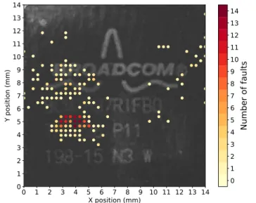
Probe spatial location. A sensitivity map has been made to find the sensitive places on the chip. By setting a high signal amplitude, we repeatedly try to inject a fault in every possible place on the chip. Next, we observe where the faults (the tested application, Listing 1, returns an incorrect result or no result at all) are obtained. The result, shown in Figure 3, clearly indicates an area of interest. 14 13 12 11 10 9 8 7 6 5 4 3 2 1 0 X position (mm) 0 1 2 3 4 5 6 7 8 9 10 11 12 13 14 Y position (mm) 0 1 2 3 4 5 6 7 8 9 10 11 12 13 14
Number of faults
Fig. 3: EMFI BCM2837 sensitivity map
(Dot size is not correlated with probe size.)
For all experiments below, the probe is placed at the most sensitive location (X = 4 mm, Y = 4.5 mm on Figure 3).
Temporal synchronization. The main difficulty for fault injection is the temporal synchronization: when to in-ject a fault on the targeted and vulnerable instructions. We first need a temporal reference, given here by a GPIO: a rising electrical edge is sent to a board pin by our application just before the area of interest. This signal is used by our apparatus to trigger the fault in-jection.
Our setup is using the evaluator approach: the at-tacker can instrument the system to ease the experi-ments. In the case of a real attack, the adversary would have to generate this trigger signal: it can be done by monitoring communications, IOs, or EM radiation to detect patterns of interest. In all cases, it is a tricky business, highly application dependent.
The trigger signal is just part of the problem: from that moment on, we must wait the correct duration to inject the fault. In other words, we want to con-trol the injection time relatively to the trigger signal, in order to inject a fault when processing the targeted
instruction. Propagation times are not negligible. On a complex CPU, the issue is more difficult due to the memory hierarchy. Since cache misses are highly unpre-dictable, they imply a corresponding jitter. It is difficult to predict the duration of memory access accurately and therefore, the waiting time to inject the fault.
Synchronization is a problem, but not an obstacle at this point. Indeed, the attacker only has to inject faults until the correct effect is achieved. Because of the jitter, for the same delay (time expected between the trigger and fault injection), different timings are tested with respect to the running program. For the same bench timing parameters, we will inject a fault during a dif-ferent instruction at each execution, but a difdif-ferent one among a small set of instructions, depending on the jit-ter. If a fault with an interesting effect is possible, it is eventually achieved.
Additionally, as we will see in the next sections, memory transfers are particularly vulnerable to EMFI. They are also slower than the core pipeline, allowing for a bigger fault injection timing window.
3.2 Forensic methodology
Contrary to the state-of-the-art fault model character-ization on complex CPUs, we target a bare-metal sys-tem, meaning that no complex OS, to characterize the effect of a fault in the micro-architecture. Removing the complex OS aims at improving the fault effect char-acterization with a better granularity by accessing to low-level micro-architecture blocks and instrumenting them.
As the targeted component is closed, we do not have any insider information and no way to analyse the hard-ware layout. Therefore, we can only characterize a fault from the instruction set architecture (ISA). Moreover, we have also limited means to explore what is happen-ing in the system, mainly the JTAG. With it, we are able to halt the chip execution to read or write the reg-ister values and to read and write memory as seen by a particular core (with a data viewpoint).
Therefore, to pinpoint the particular effects of a fault injection, we force the system state such that an observable change gives us information on the fault mechanism. In particular, we have put several cache invalidation instructions in memory. During our foren-sic process, we can therefore call them by modifying the program counter (PC) by writing directly to it with the JTAG.
A technique used to detect the fault location is to execute the suspected instructions step-by-step (with the JTAG), and the verify the side effects after each instruction (by reading memory and registers).
Our software footprint has to be minimal to main-tain controllability on the system state. As such, we will not describe how to breach a particular system with our faults since any exploit is highly application-dependent, and our setup is not representative of a stan-dard application environment. Instead, we will suggest exploit strategies: how a malicious attacker could use such faults?
A demonstration of a fault exploitation, given in sec-tion 7, is done on our own AES encrypsec-tion implemen-tation. However, those results cannot be extrapolated to any real-world application.
3.3 Characterization modus operandi
The application targeted during this experiment is two nested loops shown on Listing 1. This program is built without compiler optimizations. We set the compiler optimization level at -O0 to have better debuggable code and correspondence between C-code and gener-ated assembly. Moreover, -O0 increases the number of memory accesses. This behavior helps us to analyse them against fault attacks.
Listing 1: Loop target application
1 trigger_up();
2 wait_us(1); // wait to compensate bench latency 3 invalidate_icache();
4 for(int i = 0; i<50; i++) { 5 for(int j = 0; j<50; j++) { 6 cnt++;
7 } }
8 trigger_down();
Before running the nested for loop, we invalidate the CPU caches (line 3) to detect modifications. Our bench has a latency of 700 ns, so we can still hit this memory transfer. To be able to observe the effect of a fault on the full-timing range, a 1 µs (line 2) wait has been inserted between the trigger and the cache invalidation. Moreover, a MMU is enabled to be closer to market deployed applications.
A fault occurs when the cnt variable value at the end of the program is not equal to 2500 or if the pro-gram crash. When a fault is detected, we use the JTAG to re-execute our for loop, in the Listing 1, by directly setting the PC value at the start of the loops. Executing instruction by instruction, we monitor the expected side effects. This execution is done without fault injection.
Based on this code, we vary the injection delay. Varying the injection delay confuses different micro-architecture blocks: L1 and L2 caches and the MMU. The L1 and L2 caches are confused at 3134 ns and the MMU is targeted at 25 400 ns.
With this setup, we disclose different fault models with EM fault injection on L1I cache, on MMU and on L2 cache.
4 Fault on the instruction cache
In this experiment, we achieve a fault in the L1 instruc-tion cache (L1I).
4.1 On the impossibility to fault the instruction execution flow
Before reporting our positive results, we must report a negative one. Contrary to previous works on micro-controllers (where, e.g. instructions are replaced with a NOP instruction), we are not able to prevent or mod-ify the execution of an instruction directly. Even if we cannot be sure that no set of experimental parameters would achieve such a fault, we thoroughly explored the parameters without success.
Instead, we get faults during cache transfers, which is probably because the buses involved in these trans-fers are easily coupled with our EM probe. In the case of a minimal application that can fit in the cache, the memories are filled only once at the first execution. As a consequence, to repeatedly observe our fault, we in-validate the cache memory of interest (L1I) just before launching our application, artificially triggering a mem-ory transfer.
4.2 Forensic
As the instruction cache is invalidated before the loop of the Listing 1 is executed, the following instructions must be (re)loaded into the cache before execution. Moreover, it is this memory transfer that we target with our fault injection. By executing the same application with and without the cache invalidation and measuring the duration of the high state of the trigger, we deduce that loading instructions in the cache has an overhead of 2 µs.
To analyze the fault, we debug, without fault and step by step, the for loop through the JTAG interface. Each instruction was correctly executed except for the addinstruction, in red, at address 0x48a08 on Listing 2. Listing 2: Assembly version of the for loop (Listing 1) without optimisation. ... 0x48a04: b94017a0 ldr x0, [x29,#20] 0x48a08: 11000400 add x0, x0, #0x1 0x48a0c: b90017a0 str x0, [x29,#20] 0x48a10: b9401ba0 ldr x0, [x29,#24] 0x48a14: 11000400 add x0, x0, #0x1 0x48a18: b9001ba0 str x0, [x29,#24] 0x48a1c: b9401ba0 ldr x0, [x29,#24] 0x48a20: 7100c41f cmp x0, #0x31
0x48a24: 54ffff0d b.le 48a04 <loop+0x48> ...
By monitoring the x0 register before and after the cntincrementing instruction, in red in the Listing 2, we observe that the value is kept unchanged: the increment is not executed. Since the fault is still present after the EM injection, we can conclude that a wrong instruc-tion value is stored in L1I. We confirm this fault model by executing an L1I cache invalidation instruction ic iallu2. By re-executing our application, the fault has disappeared.
We can infer that the injected fault has affected a part of the L1I cache. However, it is impossible to ac-cess (read) the new instruction value. Since the fault happens during the cache filling, we can suppose that the memory transfer had been altered.
Moreover, this fault model matches the observation made by Trouchkine et al. in [21]. In this work, the authors characterize a fault model while perturbing a BCM2837 using EMFI. The model they observe is the corruption of the executed instruction second operand, which is forced to 0. This ISA fault model matches the one we observe in the cache as the corruption of the instruction add x0, x0, #0x1 by forcing the second operand to 0 gives the instruction add x0, x0, #0x0 which explains why the increment is not executed as we add 0 to the register. They identify that their faults happen during the instruction fetch. However, as they work with an OS, they cannot reliably test if the fault they observe is persistent in the cache, while we can with our bare-metal setup.
4.3 Exploits
This fault is one of the easiest to exploit since it in-duces an instruction replacement fault model, where an instruction is replaced by another. It can often be re-duced to the classical instruction skip model, if the new instruction has no side effects on the application. There-fore, most exploits based on this classical model apply here. Since the faulted value is still present in the cache, it will stay faulted until the cache is invalidated: we can call this model “sticky instruction skip”. Bukasa et al. [7] demonstrated applications of this fault model: hi-jacking the control flow and initiating a return-oriented programing (ROP) attack, among others.
2 We set the PC value to the ic iallu instruction address in
5 Targeting the memory management unit The MMU is a critical component of the complex CPUs. It is in charge of the virtual memory mechanism and en-sure memory partitioning between applications. In this section, the fault corrupts the virtual-to-physical mem-ory mapping albeit in an uncontrolled manner. The tar-geted application is the same as in section 4, shown in Listing 1; only the fault injection timing has changed. We inject the fault at 25 400 ns after the trigger instead of 3144 ns when the L1I is confused. The faults, ana-lyzed in this section, always crash the program in List-ing 1.
We show in this section that this delay enables to perturb the MMU micro-architectural block. Regarding the results from the other characterization works in this paper, the cache hierarchy is the most sensitive CPU micro-architectural block.
5.1 Configuration of a working MMU
To understand the fault effect on the MMU, we begin to explore the state of an application without any fault. This state is a legitimate one.
5.1.1 Page tables
The page tables are used to memorize the mapping be-tween virtual and physical memory. In our configura-tion, we have 3-page table directory (PTD) (mapping 512 MB chunks), and for each of them, we have 8 192 PTE pages of 64 kB.
In the page tables, the most and least significant bits are used for the page metadata (access rights, caches configuration, etc.).
5.1.2 Translation lookaside buffer
TLBs (plural since there are several of them) are small buffers used to speed up virtual-to-physical memory translation. As in a cache memory, the last mappings are saved from being reused later without a full-page walk by the MMU. In the targeted CPU, TLB hier-archy mirrors cache hierhier-archy: the TLB designates the unified Level2 buffer while micro-TLBs are dedicated to instructions or data in each core.
5.1.3 Operating system
In our bare-metal application, all the pages are initial-ized in the page tables with an identity mapping (vir-tual and physical addresses are identical). In a system with an OS, pages are allocated on-the-fly. On the one
hand, this simplifies the forensic analysis since we are sure that page tables are correct prior to the fault. On the other hand, interesting faults may be missed if the OS page allocation is disrupted.
5.2 Forensic
To reconstruct the memory mapping, we use a pair of instructions computing the physical address (and the corresponding metadata) for a given virtual one. A script has been designed to extract the memory map-ping. By using the JTAG, first, the two instructions at s1e3r, x0 and mrs x0, PAREL1 are written at a given address, then the x0 register is set to one virtual address, the two instructions are executed, and finally, the x0 register contains the corresponding physical ad-dress.
With this method, we compare the memory map-pings with (Table 3) and without (Table 2) a fault.
Virtual Address Physical Address
Virtual Address Physical Address 0x0 0x0 0x80000 0x80000 0x10000 0x10000 0x90000 0x90000 0x20000 0x20000 0xa0000 0xa0000 0x30000 0x30000 0xb0000 0xb0000 0x40000 0x40000 0xc0000 0xc0000 0x50000 0x50000 0xd0000 0xd0000 0x60000 0x60000 0xe0000 0xe0000 0x70000 0x70000 0xf0000 0xf0000
Table 2: Correct identity mapping
Virtual Address Physical Address
Virtual Address Physical Address 0x0 0x0 0x80000 0x0 0x10000 0x10000 0x90000 0x0 0x20000 0x20000 0xa0000 0x0 0x30000 0x30000 0xb0000 0x0 0x40000 0x40000 0xc0000 0x80000 0x50000 0x50000 0xd0000 0x90000 0x60000 0x60000 0xe0000 0xa0000 0x70000 0x70000 0xf0000 0xb0000
Table 3: Mapping after fault
Three different effects can be observed depending on the page:
1. Pages are correct with an identity mapping up to 0x70000. Remarkably, these are all the pages used to map our application in memory. Therefore, a hy-pothesis is that the corresponding translations are present in caches and are not impacted by the fault (in green in Table 3).
2. Pages are incorrectly mapped to 0x0. For instance, a read at 0x80000 reads, with success, physical mem-ory at 0x0 (in blue in Table 3).
3. Pages are shifted. For example, a read at 0xc0000 gives the physical memory value at 0x80000 (in red in Table 3).
If we invalidate the TLB after a fault, nothing changes: the mapping is still modified. We conclude that the fault does not affect the cache mechanism to address transla-tion (at least what can be invalidated by software) but directly the MMU configuration.
The fault on the MMU shifts the page tables in memory and inserts errors on it. The tables are still present, with small modifications, but at another base address.
Since the memory translation is still valid after the fault (translations are considered valid by the CPU), and do not correspond to the shifted page tables (we can reconstruct the virtual to physical mapping from the new page tables), this shift is not the only source of incorrect translation. Finally, we do not have enough control over the CPU to observe the failure cause with precision.
5.3 Exploit
This fault shows that the cornerstone of the key security feature in any CPU, namely memory isolation, does not withstand fault injection. In [23], the authors use the Rowhammer attack to fault a PTE. The faulted PTE accesses the kernel memory, which allows the attacker to obtain a privilege escalation: by overwriting a user-land PTE for accessing all the memory, by changing the user ID to root or by changing the entry point of an executable.
Additionally, this fault model is a threat to pointer authentication countermeasures, as proposed in the re-cent ARMv8.3 ISA. This pointer protection mechanism works by storing authentication metadata in the most significant bits (usually useless) of a pointer value. The chip first validates the authentication metadata in or-der to use a pointer. In our case, the attacker does not need to alter the pointer value; it can alter where it physically points to, at a coarse (page) granularity.
6 Shifting data chunks in L2
We showed that the attacker could inject faults in the L1I cache and the MMU. In this section, we will demon-strate that another cache memory can be targeted: the L2 cache.
Another interesting behavior when faulting a modi-fied version of the loop target, c.f. Listing 3, was inves-tigated with JTAG.
The initial goal was to try to modify register values to see if we could confirm the fault model as in [21]. Instead, we observed an original behavior described in this section. Inside each loop iteration, we call a func-tion, register_transfer, that self copies all registers (e.g., mov x1, x1). init_registers fills registers x0 to x7 with constants (9 instructions with the ret). Listing 3: Assembly for the modified loop target, the
framed instructions have been added with respect to Listing 2. We also show the instructions just before in our function. 0x489bc: a9be7bfd stp x29, x30, [sp,#-32]! 0x489c0: 910003fd mov x29, sp 0x489c4: b9001fbf str wzr, [x29,#28] 0x489c8: b9001bbf str wzr, [x29,#24] 0x489cc: b90017bf str wzr, [x29,#20] 0x489d0: 900001a0 adrp x0, 7c000 <RT2+0xb0> 0x489d4: 912d2000 add x0, x0, #0xb48 0x489d8: d2802002 mov x2, #0x100 0x489dc: 52800001 mov w1, #0x0 0x489e0: 94000b28 bl 4b680 <memset> 0x489e4: 97fefe67 bl 8380 <fast_trig_up> 0x489e8: d2800040 mov x0, #0x2
0x489ec: 97feffe2 bl 8974 <wait_us>
0x489f0: 94008765 bl 6a784 <invalidate_icache> 0x489f4: 940087ad bl 6a8a8 <init_registers> 0x489f8: b9001fbf str wzr, [x29,#28] 0x489fc: 14000010 b 48a3c <loop+0x80>
0x48a00: b9001bbf str wzr, [x29,#24] 0x48a04: 14000008 b 48a24 <loop+0x68>
0x48a08: 940087c1 bl 6a90c <register_transfer> 0x48a0c: b94017a0 ldr w0, [x29,#20] 0x48a10: 11000400 add w0, w0, #0x1 0x48a14: b90017a0 str w0, [x29,#20] 0x48a18: b9401ba0 ldr w0, [x29,#24] 0x48a1c: 11000400 add w0, w0, #0x1 0x48a20: b9001ba0 str w0, [x29,#24] 0x48a24: b9401ba0 ldr w0, [x29,#24] 0x48a28: 7100c41f cmp w0, #0x31
0x48a2c: 54fffeed b.le 48a08 <loop+0x4c>
The pulse parameters are strictly identical to the ones used for injecting a fault on L1I (in particular, we have the same delay of 3144 ns). But the different observed behaviors may be explained by the modifica-tion of the program under test (framed instrucmodifica-tions in Listing 3). This modification has, in our opinion, no ef-fect on the fault due to the functionality, but instead because it modifies the cache timings.
We show in this section that data are shifted in the L2 cache as if addresses had been slightly modified in the transfer from RAM to L2.
6.1 Forensic
6.1.1 Cache coherency methodology
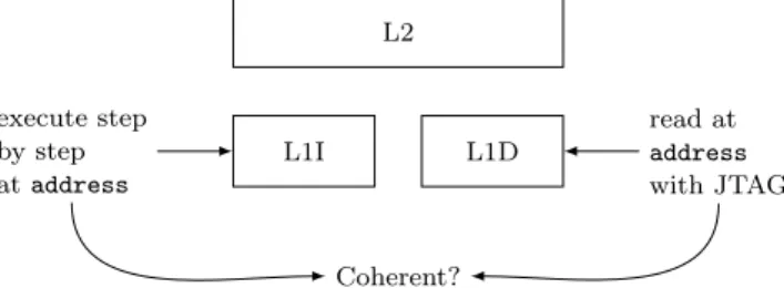
The difficulty to identify the presence of a fault in the cache L2 is that we cannot observe it. Instead, we will locate the fault indirectly by testing the coherency of the L1I, L1D and L2 caches with the methods illus-trated in Figures 4, 5 and 6.
First, to check the coherency of L1D and L1I, we use the JTAG as illustrated on Figure 4. We compare the instructions read from L1D with the JTAG with the ones executed (fetched from L1I) by checking on their side effects, one instruction at a time.
L2 L1I L1D read at address with JTAG execute step by step at address Coherent?
Fig. 4: Method for testing cache coherency between L1D and L1I using JTAG
Next, to verify the coherency of L1D with respect to L2, we force a new fetch from L2 after invalidating L1D as illustrated on Figure 5.
L2
L1I L1D
1. Read with JTAG 2. Invalidate 3. Read = first read? Fetch on2ndread
Fig. 5: Method for testing cache coherency between L1D and L2 using JTAG
Finally, it is also possible to force a new fetch from L2 after invalidating L1I (cf. Figure 6). We compare the executions before and after this new fetch by executing instructions step-by-step.
6.1.2 Incoherent cache fault
With the same injection parameters as in section 5, we can achieve a new reproducible faulted behavior where the chip is trapped in an infinite loop, as seen with a step-by-step execution. However, when we repeat
L2
L1I L1D 1. Execute
2. Invalidate
3. Execute = first execution?
Fetch on2ndexecution
Fig. 6: Method for testing cache coherency between L1I and L2 using JTAG
the fault and observe the dumps with JTAG, we have two observable states (both are reproducible), called CoherentState and IncoherentState, that differ by the data read in L1D.
A JTAG memory dump (from L1D point of view) at the instruction memory location for CoherentState shows modified instructions as seen on Listing 4a, to be compared to the unfaulted dump on Listing 4b.
The dump for IncoherentState shows different val-ues in L1D memory with respect to CoherentState (for the first two instructions), as seen on the Listing 5. Listing 5: Memory dump showing the instructions in the infinite loop as seen by the JTAG (L1D point of view) for IncoherentState.
0x000489f8: 940087c1 b94017a0 11000400 b90017a0
0x00048a08: b9401ba0 11000400 b9001ba0 b9401ba0
0x00048a18: 7100c41f 54fffeed b9401fa0 11000400 0x00048a28: b9001fa0 b9401fa0 7100c41f 54fffded
The step-by-step execution is coherent with the in-structions shown by the JTAG dump for CoherentState (registers are loaded, stored and incremented as speci-fied in this dump), which means that L1I and L1D are identically faulted. Therefore, we can suppose that the fault is present in the L2 cache (the first unified cache). The reconstructed instructions can be seen in Listing 6.
Listing 6: Assembly reconstruction of the faulted in-structions from the Listing 4a.
address binary value Instruction
0x489f8: b9001bbf str wzr, [x29,#24] 0x489fc: b90017bf str wzr, [x29,#20] 0x48a00: 11000400 add w0, w0, #0x1 0x48a04: b90017a0 str w0, [x29,#20] 0x48a08: b9401ba0 ldr w0, [x29,#24] 0x48a0c: 11000400 add w0, w0, #0x1 0x48a10: b9001ba0 str w0, [x29,#24] 0x48a14: b9401ba0 ldr w0, [x29,#24] 0x48a18: 7100c41f cmp w0, #0x31 0x48a1c: 54fffeed b.le 489f8
0x489d8: d2800040 97feffe2 00000002 00000008 0x489e8: 00000002 00000008 910003fd b9001fbf
0x489f8: b9001bbf b90017bf 11000400 b90017a0
0x48a08: b9401ba0 11000400 b9001ba0 b9401ba0
0x48a18: 7100c41f 54fffeed b9401fa0 11000400 0x48a28: b9001fa0 b9401fa0 81040814 77777777 (a) Memory dump showing the instructions as seen by the JTAG (L1D point of view) for CoherentState. The instruc-tions in the infinite loop are underlined.
0x489b8: d65f03c0 a9be7bfd 910003fd b9001fbf
0x489c8: b9001bbf b90017bf 900001a0 912d2000 0x489d8: d2802002 52800001 94000b28 97fefe67 0x489e8: d2800040 97feffe2 94008765 940087ad 0x489f8: b9001fbf 14000010 b9001bbf 14000008
0x48a08: 940087c1 b94017a0 11000400 b90017a0
0x48a18: b9401ba0 11000400 b9001ba0 b9401ba0
0x48a28: 7100c41f 54fffeed b9401fa0 11000400 (b) Memory dump showing correct (without fault) instruc-tions for the same memory region.
Listing 4: Comparison of the memory dumps with and without fault.
It is impossible to observe the L2 cache content, we must therefore confirm our hypothesis with additional indirect evidence, using our methodology introduced in section 6.1.1.
L1 fault. The L1I is modified by the fault since the behavior of the application is modified. However, the execution is coherent with the JTAG dump (showing the L1D cache) for CoherentState, hinting that L2 is impacted too.
In this case, if we invalidate the whole L1I cache (with ic iallu instruction), as illustrated on Figure 6, nothing changes (either in the execution trace or in the JTAG dump).
For IncoherentState, 940087c1 (first brown in-struction in Listing 5) encodes a direct unconditional jump (bl) instruction that is not followed in the step-by-step execution. Therefore, in this case the JTAG dump (corresponding to data in L1D) does not reflect the values in the L1I cache. However, if we invalidate a cache line of L1D at address 0x489f8 (with dc ivac instruction), as illustrated on Figure 5, then L1D is modified, as seen with JTAG, and becomes the same as for CoherentState. Therefore, the L1D data seen in CoherentStateis present in L2.
However, to the best of our knowledge, it is not pos-sible to directly invalidate the L2 cache to directly con-firm our hypothesis.
memory management unit. A possibility that would ex-plain coherent faults in L1D and L1I but not L2 is a modification of the memory mapping if the fault im-pacted the MMU.
After verification as in section 5, we observe that the MMU mapping is indeed modified but not for the mem-ory region of interest. In particular, memmem-ory addresses from 0x0 to 0x7FFFF are still correctly mapping iden-tically virtual and physical addresses. The fault on the MMU cannot, therefore, explain our observations.
Hypotheses. The effect of these faults seems to manifest itself in the L2 cache. We can observe that it consists in shifting groups of 4 instructions (128 bits or 16 B, under the cache line size of 64 B) at a nearby memory location. 128-bit is the size of the external memory bus connected to L2. The fault model could be that the address corresponding to a cache transfer toward L2 has been modified by a few bits.
Our model has some limits: with one fault, values in L2 and in L1D are modified simultaneously in an incoherent way for IncoherentState. Is it due to the EM probe coupling with several buses or to a micro-architectural mechanism?
6.2 Exploits
A fault in the L2 cache can impact either the instruc-tions or the data giving more power to the attacker. Nevertheless, she does not control in what way the memory will be modified. Why have these particular 16-byte blocks been shifted? Nevertheless, just corrupting data or instruction randomly is often enough to achieve the desired effect (as in the NOP fault model).
7 When persistent fault analysis meets L1D cache
To demonstrate the applicability of a cache memory fault model, a persistent fault analysis (PFA) [29] is performed on a bare-metal AES implementation. In this section, we show how to reduce the AES key to 224
possibilities instead of 2128
, with one persistent fault in L1D.
7.1 Setup
With the same experimental setup as before, we now target an AES encryption. Our AES implementation is
a naive one without countermeasures. The sboxes are implemented with a lookup table. Before the actual en-cryption, we pre-warm the cipher: in order to limit tim-ing leakages due to caches, we first invalidate L1I and L1D. Then we perform a dummy AES encryption to fill the caches with data and instructions of interest. This is the step where we inject the fault.
In a second step, we encrypt 10 000 random plain-texts, without any new fault injection, and try to de-duce the key from the observed (faulty) ciphertexts.
7.2 Persistent fault analysis: the theory
We target the sbox lookup table: by modifying at least one bit in the table, the operation is now biased. For example, for the input x, the output is now
y∗= SB∗(x), (1)
instead of y = SB(x).
Since a sbox is a bijection, now y cannot be out-putted by SB∗, the faulted sbox. We say that y is
for-bidden. At the last round of the AES encryption, for each byte index i ∈ [[0, 15]], we have
SB∗(x
i) ⊕ K10i= Ci∗, (2)
where x is an intermediate state, K10 the last round key and C∗ the faulty ciphertext. We consider, as an
approximation, that the distribution of xi is uniform
for all i.
Since y is a forbidden value, y ⊕ K10i cannot be
ob-served as a result for any C∗
i and this for all byte index
i∈ [[0, 15]]. We note C0
i the forbidden value for the
cor-responding ciphertext at byte index i. The attacker can easily observe C0
i, it is enough to count the occurrences
of the byte values and find the specific one that never occurs.
While we try to guess for the forbidden value y (28
possibilities), we can compute:
∀i, K10i= C 0
i ⊕ y. (3)
From there, the master key is trivially recovered from K10, and a known pair with a plaintext and the corresponding correct ciphertext allows the attacker to validate the correct guess.
7.3 Results
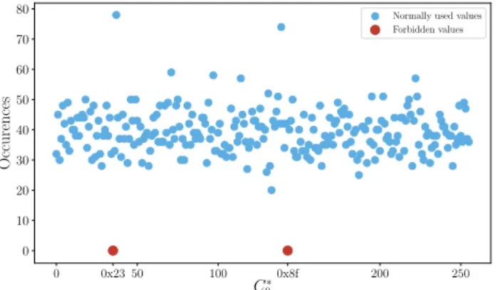
In order to detect the forbidden values, we simply count the number of occurrences for all bytes values in the ci-phertext, for the first byte, then the second byte, etc.
On Figure 7, we can observe that 2-byte values are forbidden. Therefore, in our case, two bytes have been faulted in the sbox lookup table.
0 0x2350 100 0x8f 200 250 C∗ 0 0 10 20 30 40 50 60 70 80 Occurences
Normally used values Forbidden values
Fig. 7: For the first ciphertext byte, a number of occur-rences for each value; for a total of 10000 occuroccur-rences.
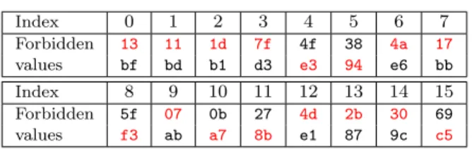
The analysis has to be adapted to the two faults case. For each byte index from 0 to 15, we get the two ciphertext forbidden values, as shown in Table 4.
Index 0 1 2 3 4 5 6 7 Forbidden 23 21 2d 4f 7f 08 7a 27 values 8f 8d 81 e3 d3 a4 d6 8b Index 8 9 10 11 12 13 14 15 Forbidden 6f 37 3b 17 7d 1b 00 59 values c3 9b 97 bb d1 b7 ac f5
Table 4: Ciphertext forbidden values. For each byte in-dex, we have 2 forbidden values. The first two forbidden values are the ones that we can observe in Figure 7.
Since we have 2 forbidden values y1and y2, we need
to create 224
hypotheses to recover the key. First, we have 28
guesses for y1 then, for each guess, we need
to choose one value out of two possibilities for each of the byte index (216
possible choices). The possible key bytes for a correctly guessed forbidden value y1 = 30
are displayed in Table 5. In other words, Table 5 is Table 4 xored with y1. Finding the key then consists in
choosing the correct value (shown in red on Table 5) out of the two, for each byte index.
In total, we have 224
key hypotheses, with a pair of plaintext and corresponding ciphertext to validate the correct key, recovering the AES key can be done on a desktop computer in a few minutes. It takes 145 s on an Intel E5-1620 v3 CPU to find y1= 30, so it would take
by extrapolation 757 s, or less than fifteen minutes, to test all keys.
Index 0 1 2 3 4 5 6 7 Forbidden 13 11 1d 7f 4f 38 4a 17 values bf bd b1 d3 e3 94 e6 bb Index 8 9 10 11 12 13 14 15 Forbidden 5f 07 0b 27 4d 2b 30 69 values f3 ab a7 8b e1 87 9c c5
Table 5: Possible key bytes for the correct guess y1 =
30. The correct K10 key is 13 11 1d 7f e3 94 4a 17 f3 07 a7 8b 4d 2b 30 c5.
7.4 Forensic
The fault exploited here is actually in L1D and can be directly observed with the JTAG. We show on Listings 7 and 8 the correct and faulty lookup tables as seen by the JTAG.
0x0006b510: 7b777c63 c56f6bf2 2b670130 76abd7fe 0x0006b520: 7dc982ca f04759fa afa2d4ad c072a49c
Listing 7: Part of the correct sbox lookup table.
0x0006b510: 7b777c63 c56f6bf2 2b670136 76abd7fe 0x0006b520: 7dc982ca f04759fa afa2d4ad c072a498
Listing 8: Part of the faulty sbox lookup table. The two faults are displayed in red.
We can notice that the sbox output 30 has been replaced by 36. 30 is, therefore, a forbidden value at sbox output, at the origin of the correct guess y1= 30.
The two faulted values are more than 128 bits apart, but on the same cache line (if we suppose that they are aligned in memory). The only memory bus (cf. Table 1) with a size greater than 128 bits is the one that write L2 from L1D values. Since we are reading sbox values, not writing them, it is highly improbable that such a bus transfer was hit. Instead, we should consider that the fault impacted several memory transfers, which has been shown possible in section 6 by the incoherence be-tween the L2 and L1D caches in the IncoherentState case.
8 Defense mechanisms
In this paper, we have shown that you cannot rely on hardware for critical functionality. Our forensic analy-ses show that the memory hierarchy and the MMU can easily be corrupted. However, other micro-architectural elements might also be confused by the injected fault.
We can conjecture that the subsystems ensuring data coherence, speculative execution, etc. will one day be the victims of fault attacks.
As such, protecting a CPU against fault attacks re-quires to ensure the integrity of their micro-architectural blocks. If this problem is well known for secure compo-nents such as smartcards, hardening blocks which com-pose a modern and complex CPU is an open problem.
In this section, we discuss how to protect complex CPUs to fault injection attacks inside the CPU or out of it through the SoC organization.
8.1 Inside the CPU
Instead of solving the integrity problem for all micro-architectural blocks, which is a complex research pro-gram in itself, we focus on the cache memories. 8.1.1 Ensuring integrity and authenticity in cache memories
Two strategies can be deployed to detect memory faults. On the one hand, a common solution to quickly verify data integrity in memory hierarchy is the error correct-ing codes (ECCs). They are efficient to detect a a lim-ited number random faults : this solution is relatively low-cost but assumes that the attacker has no control over the fault value and cannot inject a lot of faults. In the other case, the attacker would be able to inject random faults until one passes the ECC scheme.
If we only consider the attacks introduced in this pa-per, this mechanism is enough due to the lack of con-trol on the fault injection and the low automation of the forensic process; the fault rate is low if we need to check the fault effects. However, face a more powerful attacker, it can only slightly slow the attack down.
On the other hand, the use of cryptography in the form of one message authentication code (MAC) can detect memory faults. A generic solution is KECCAK message authentication code (KMAC) with a small out-put length since the lifetime of the integrity and authen-ticity protection is limited and to reduce the memory overhead. With an output length of 64 bits (we store 8 B of MAC for each 64 B cache line), the protection increases by 12.5% the memory footprint than the un-protected version (without taking into account tags and flags).
Key generation. The key k is a true random value that the system should generate at boot time. It must be kept secret so that the attacker cannot know the correct MAC value for a given cache line.
Signing. For each cache line modification, total or par-tial, the KMAC must be computed again. For a cache line tag t, data block d and flags f let h = KM AC(k, t|d|f ) be the MAC value stored along the cache line. Instead of the tuple (t, d, f ), we now store (t, d, f, h).
Verifying. When a cache line is read, the MAC must be verified. For a read in the cache line constituted by the tuple (t, d, f, h), we compute hverif = KM AC(k, t|d|f ).
Finally, we compare h and hverif. If they are equal, the
read value is correct. Otherwise, we trigger the alarm: an exception is raised to allow custom software man-agement.
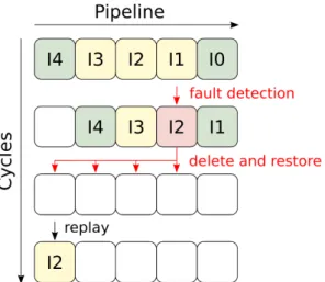
8.1.2 Speculative memory accesses
To ensure data integrity, a MAC is necessary against powerful attackers. However, computing a KMAC re-quires multiple cycles which drastically decrease the performances of the whole system, especially in the memory hierarchy which already constitutes a bottle-neck.
To tackle this problem, we introduce a speculative mechanism for integrity verification. By default, all data coming from memory are considered as usable but not verified : we speculate that they are correct. Therefore, load instructions must be dealt with similarly to specu-lative branches: the core can continue its execution, but without committing the load until the integrity verifica-tion. If the chip is under attack, the verification would fail and the chip can be restored to its initial state, before the incriminated load.
Fig. 8: Integrity speculation in a pipelined core. A green instruction means that no speculation is involved, a yel-low one that speculation is pending. The red instruction denotes a speculative load that is dismissed.
Figure 8 illustrates with an example how integrity speculation can be managed in a pipelined core.
With this speculation strategy, verification and nor-mal computation can be performed simultaneously. It allows increasing the latency margin to perform the verification, enabling the use of MACs. Obviously, this kind of mechanism would be made simpler and less crit-ical by low latency cryptographic hashes, which have yet to be invented.
8.1.3 The path to secure cores
Complex cores today are mainly split into two classes, the high-performance ones and the low energy consump-tion ones. The security problems are addressed through software modification (e.g. retpoline [22] against the Spectre attack [11]) or minimal hardware modification (e.g. TrustZone to protect against rich OS vulnerabili-ties). Security is considered as an implementation issue, where attacks happen only if a designer made a mistake. However, this work shows that a modern complex core is not a reliable substrate for secure computations. Generic secure cores must be designed to handle all the security needs. These secure cores will have to be de-signed from the ground up, to guarantee security prop-erties across all micro-architectural blocks. We envision a future where the SoCs will be composed of 3 kinds of cores: a core can either grant high performance, low energy consumption or high security.
8.2 Through the SoC organization
It is worth mentioning a natural countermeasure that may complicate fault attacks on SoCs, 3D packaging. This technique consists in stacking the dies (CPU, mem-ory, baseband, etc.) in the same package. Experimen-tally, the attacker may find it difficult to target dies that are not on the surface of the package. Yet it has been demonstrated possible: for example, Vasselle et al. [25] show a laser fault injection attack on a SoC where the external RAM is stacked on it.
9 Related works
In the literature, fault attacks are a hot topic where studies are focused on effects, targetting both MCUs and complex CPUs. Despite the works made on MCUs, recent complex CPUs are still vulnerable to fault at-tacks mainly because the manufacturers prefer perfor-mance or low consumption than security [11, 12]. In this section, we made an overview of state-of-the-art fault
attacks.
Fault attacks on hardware components have been studied starting from the seminal work of Skoroboga-tov et al. [17] in 2002. Significant works which focus on MCUs have been devoted to demonstrating how fault attacks can break security mechanisms where both cryptography [16, 24, 27] and critical applications [3, 5] are targeted.
Until recently, MCUs were the favourite targets since they are cheaper and simpler (no memory virtualiza-tion, simple cache levels if any, no speculative nor out-of-order execution) than the complex CPUs. Therefore, it was a good target to evaluate the fault effects. Mainly within a black box approach, several works [1, 2, 10, 13, 15, 26] focus on characterizing fault effects from the ISA level. Characterizing ISA faults is an interesting approach when you have no access to the hardware IP. Another approach [4, 9] is to focus on characterizing faults at the level of transistors and logic gates.
Recently, inspired by the works made on MCUs, fault attacks targeting complex CPUs have emerged. They target the secure boot [8, 20, 25], the trusted exe-cution environment (TEE) [18], the memory partition-ing [23] or some OS security mechanisms [19]. However, due to the complexity of both hardware and software on these targets, characterizing the fault effects are more difficult than on MCUs.
Characterizing fault effects on complex CPUs is a hot topic to improve their hardware security; for in-stance, to prevent attacks by implementing efficient coun-termeasures. Few works [14, 21] focus on this research area.
In [14], the authors develop a fault model at the ISA level. In other words, they identify how the data and the instructions of a program are affected by the fault. It is essential to understand the impact on a pro-gram and to propose software-based countermeasures, but some works have shown that software-based coun-termeasures are not sufficient [27] and hardware ones are needed. However, for building hardware counter-measures, the fault model must be characterized at the micro-architectural level, not the ISA level.
To complete this approach, Trouchkine et al. [21] propose a model for complex CPUs and a method to ob-tain micro-architectural information on the fault from observations at the ISA level. By using this method, the authors are able to identify the defects that appear in the registers, pipeline or cache of an x86 CPU and an ARM CPU. Although this method is able to iden-tify the affected CPU micro-architectural components,
due to the complex OS presence and from an ISA per-spective, they are not able to accurately determine the micro-architectural fault model.
In our article, we focus on a target without a com-plex OS. Therefore, we relax hypotheses about the ef-fect of a complex software on the fault efef-fect charac-terization. Within this approach, we disclose new fault effects on the memory hierarchy.
10 Conclusion
In this paper, we have demonstrated that complex CPUs are vulnerable to fault injection attacks. In particular, the memory hierarchy and the MMU can be changed, which creates a mismatch between hardware behavior and software expectations. Nowadays, the security of computing systems is focused on the software side; there are no efficient countermeasures against hardware per-turbations in complex CPUs. Pointer authentication, as proposed by the ARMv8.3 ISA, for example, does not resist the introduced fault model.
Exploitation heavily depends on the interaction be-tween the hardware (the specific device) and the soft-ware (including applications and OS). Therefore the cautious developer cannot predict where vulnerabilities will occur and, as a consequence, cannot efficiently pro-tect its application. Today, such attacks using EMFI are still quite hard to realize: they require expensive ap-paratus, human resources to do the experiments, etc. However, they are within reach of small organizations, and we can expect that the difficulty and cost of these attacks will be lower in the future.
Actions must be taken to ensure that computing sys-tems handle sensitive information securely. The perfor-mances/energy consumption trade-off has been settled by implementing the two kinds of cores in the same SoC. In the same way, we need secure cores as well that com-promise both on performances and energy consumption but can offer much stronger security guarantees.
References
1. J. Balasch, B. Gierlichs, and I. Verbauwhede. An in-depth and black-box characterization of the ef-fects of clock glitches on 8-bit mcus. In 2011 Work-shop on Fault Diagnosis and Tolerance in Cryptog-raphy, FDTC 2011, Tokyo, Japan, September 29, 2011, pages 105–114, 2011.
2. H. Bar-El, H. Choukri, D. Naccache, M. Tunstall, and C. Whelan. The sorcerer’s apprentice guide to fault attacks. Proc. IEEE, 94(2):370–382, 2006.
3. G. Barbu, H. Thiebeauld, and V. Guerin. Attacks on java card 3.0 combining fault and logical at-tacks. In D. Gollmann, J. Lanet, and J. Iguchi-Cartigny, editors, Smart Card Research and Ad-vanced Application, 9th IFIP WG 8.8/11.2 Inter-national Conference, CARDIS 2010, Passau, Ger-many, April 14-16, 2010. Proceedings, volume 6035 of Lecture Notes in Computer Science, pages 148– 163. Springer, 2010.
4. N. Beringuier-Boher, M. Lacruche, D. El-Baze, J. Dutertre, J. Rigaud, and P. Maurine. Body bi-asing injection attacks in practice. In M. Palkovic, G. Agosta, A. Barenghi, I. Koren, and G. Pelosi, editors, Proceedings of the Third Workshop on Cryptography and Security in Computing Systems, CS2@HiPEAC, Prague, Czech Republic, January 20, 2016, pages 49–54. ACM, 2016.
5. G. Bouffard, J. Iguchi-Cartigny, and J. Lanet. Combined software and hardware attacks on the java card control flow. In E. Prouff, editor, Smart Card Research and Advanced Applications -10th IFIP WG 8.8/11.2 International Conference, CARDIS 2011, Leuven, Belgium, September 14-16, 2011, Revised Selected Papers, volume 7079 of Lec-ture Notes in Computer Science, pages 283–296. Springer, 2011.
6. L. Breveglieri, S. Guilley, I. Koren, D. Naccache, and J. Takahashi, editors. 2011 Workshop on Fault Diagnosis and Tolerance in Cryptography, FDTC 2011, Tokyo, Japan, September 29, 2011. IEEE Computer Society, 2011.
7. S. K. Bukasa, R. Lashermes, J.-L. Lanet, and A. Legay. Let’s shock our iot’s heart: Armv7-m under (fault) attacks. In Proceedings of the 13th International Conference on Availability, Reliabil-ity and SecurReliabil-ity, ARES 2018, pages 33:1–33:6, New York, NY, USA, 2018. ACM.
8. A. Cui and R. Housley. BADFET: Defeating Mod-ern Secure Boot Using Second-Order Pulsed Elec-tromagnetic Fault Injection. In W. Enck and C. Mulliner, editors, 11th USENIX Workshop on Offensive Technologies, WOOT 2017, Vancouver, BC, Canada, August 14-15, 2017. USENIX Asso-ciation, 2017.
9. M. Dumont, M. Lisart, and P. Maurine. Electro-magnetic fault injection : How faults occur. In 2019 Workshop on Fault Diagnosis and Tolerance in Cryptography, FDTC 2019, Atlanta, GA, USA, August 24, 2019, pages 9–16. IEEE, 2019.
10. L. Dureuil, M. Potet, P. de Choudens, C. Dumas, and J. Clédière. From code review to fault injection attacks: Filling the gap using fault model inference. In N. Homma and M. Medwed, editors, Smart Card
Research and Advanced Applications - 14th Inter-national Conference, CARDIS 2015, Bochum, Ger-many, November 4-6, 2015. Revised Selected Pa-pers, volume 9514 of Lecture Notes in Computer Science, pages 107–124. Springer, 2015.
11. P. Kocher, J. Horn, A. Fogh, D. Genkin, D. Gruss, W. Haas, M. Hamburg, M. Lipp, S. Mangard, T. Prescher, et al. Spectre attacks: Exploiting spec-ulative execution. In 2019 IEEE Symposium on Se-curity and Privacy (SP), pages 1–19. IEEE, 2019. 12. M. Lipp, M. Schwarz, D. Gruss, T. Prescher,
W. Haas, A. Fogh, J. Horn, S. Mangard, P. Kocher, D. Genkin, Y. Yarom, and M. Hamburg. Melt-down: Reading kernel memory from user space. In W. Enck and A. P. Felt, editors, 27th USENIX Se-curity Symposium, USENIX SeSe-curity 2018, Balti-more, MD, USA, August 15-17, 2018, pages 973– 990. USENIX Association, 2018.
13. N. Moro, A. Dehbaoui, K. Heydemann, B. Robis-son, and E. Encrenaz. Electromagnetic fault in-jection: Towards a fault model on a 32-bit micro-controller. In 2013 Workshop on Fault Diagnosis and Tolerance in Cryptography, Los Alamitos, CA, USA, August 20, 2013, pages 77–88, 2013.
14. J. Proy, K. Heydemann, F. Majéric, A. Berzati, and A. Cohen. A first isa-level characterization of em pulse effects on superscalar microarchitectures – a secure software perspective. In ARES 2019, 2019. 15. L. Rivière, Z. Najm, P. Rauzy, J. Danger,
J. Bringer, and L. Sauvage. High precision fault injections on the instruction cache of armv7-m architectures. In IEEE International Symposium on Hardware Oriented Security and Trust, HOST 2015, Washington, DC, USA, 5-7 May, 2015, pages 62–67, 2015.
16. J. Schmidt and C. Herbst. A practical fault at-tack on square and multiply. In L. Breveglieri, S. Gueron, I. Koren, D. Naccache, and J. Seifert, ed-itors, Fifth International Workshop on Fault Diag-nosis and Tolerance in Cryptography, 2008, FDTC 2008, Washington, DC, USA, 10 August 2008, pages 53–58. IEEE Computer Society, 2008. 17. S. P. Skorobogatov and R. J. Anderson. Optical
fault induction attacks. In B. S. K. Jr., Ç. K. Koç, and C. Paar, editors, Cryptographic Hardware and Embedded Systems - CHES 2002, 4th International Workshop, Redwood Shores, CA, USA, August 13-15, 2002, Revised Papers, volume 2523 of Lecture Notes in Computer Science, pages 2–12. Springer, 2002.
18. A. Tang, S. Sethumadhavan, and S. J. Stolfo. CLKSCREW: exposing the perils of security-oblivious energy management. In E. Kirda and
T. Ristenpart, editors, 26th USENIX Security Sym-posium, USENIX Security 2017, Vancouver, BC, Canada, August 16-18, 2017., pages 1057–1074. USENIX Association, 2017.
19. N. Timmers and C. Mune. Escalating privileges in linux using voltage fault injection. In 2017 Work-shop on Fault Diagnosis and Tolerance in Cryptog-raphy, FDTC 2017, Taipei, Taiwan, September 25, 2017, pages 1–8. IEEE Computer Society, 2017. 20. N. Timmers, A. Spruyt, and M. Witteman.
Con-trolling PC on ARM using fault injection. In 2016 Workshop on Fault Diagnosis and Tolerance in Cryptography, FDTC 2016, Santa Barbara, CA, USA, August 16, 2016, pages 25–35, 2016.
21. T. Trouchkine, G. Bouffard, and J. Clediere. Fault Injection Characterization on modern CPUs – From the ISA to the Micro-Architecture. In WISTP 2019, Paris, France, 2019.
22. P. Turner. Retpoline: a software construct for preventing branch-target-injection. https: // support. google. com/ faqs/ answer/ 7625886, 2018.
23. V. van der Veen, Y. Fratantonio, M. Lindorfer, D. Gruss, C. Maurice, G. Vigna, H. Bos, K. Razavi, and C. Giuffrida. Drammer: Deterministic rowham-mer attacks on mobile platforms. In Proceedings of the 2016 ACM SIGSAC Conference on Com-puter and Communications Security, Vienna, Aus-tria, October 24-28, 2016, pages 1675–1689, 2016. 24. J. G. J. van Woudenberg, M. F. Witteman, and
F. Menarini. Practical optical fault injection on secure microcontrollers. In Breveglieri et al. [6], pages 91–99.
25. A. Vasselle, H. Thiebeauld, Q. Maouhoub, A. Morisset, and S. Ermeneux. Laser-induced fault injection on smartphone bypassing the secure boot. In 2017 Workshop on Fault Diagnosis and Toler-ance in Cryptography, FDTC 2017, Taipei, Taiwan, September 25, 2017, pages 41–48, 2017.
26. I. Verbauwhede, D. Karaklajic, and J. Schmidt. The fault attack jungle - A classification model to guide you. In Breveglieri et al. [6], pages 3–8. 27. B. Yuce, N. F. Ghalaty, H. Santapuri, C.
Desh-pande, C. Patrick, and P. Schaumont. Software fault resistance is futile: Effective single-glitch at-tacks. In 2016 Workshop on Fault Diagnosis and Tolerance in Cryptography, FDTC 2016, Santa Barbara, CA, USA, August 16, 2016, pages 47–58. IEEE Computer Society, 2016.
28. B. Yuce, P. Schaumont, and M. Witteman. Fault attacks on secure embedded software: Threats, de-sign, and evaluation. Journal of Hardware and Sys-tems Security, 2(2):111–130, Jun 2018.
29. F. Zhang, X. Lou, X. Zhao, S. Bhasin, W. He, R. Ding, S. Qureshi, and K. Ren. Persistent fault analysis on block ciphers. IACR Transactions on Cryptographic Hardware and Embedded Systems, 2018(3):150–172, Aug. 2018.