HAL Id: hal-01879173
https://hal.archives-ouvertes.fr/hal-01879173
Submitted on 22 Sep 2018
HAL is a multi-disciplinary open access
archive for the deposit and dissemination of
sci-entific research documents, whether they are
pub-lished or not. The documents may come from
teaching and research institutions in France or
abroad, or from public or private research centers.
L’archive ouverte pluridisciplinaire HAL, est
destinée au dépôt et à la diffusion de documents
scientifiques de niveau recherche, publiés ou non,
émanant des établissements d’enseignement et de
recherche français ou étrangers, des laboratoires
publics ou privés.
Benattou Sadani, Salvatore Pes, Sophie Bouchoule, Laurent Dupont,
Jean-Baptiste Doucet, Mehdi Alouini, et al.
To cite this version:
Christophe Levallois, Cyril Paranthoen, Benjamin Boisnard, Thierry Camps, Benattou Sadani,
et al.. Liquid crystal based tunable PIN-photodiodes for detection around 1.55-µm. SPIE
Op-tics+Photonics - Nanoscience+Engineering 2018, Aug 2018, San Diego, United States. pp.107290H,
�10.1117/12.2322138�. �hal-01879173�
Liquid Crystal based Tunable PIN-Photodiodes for detection around
1.55-µm
C. Levallois*
a, C. Paranthoen
a, B. Boisnard
b, T. Camps
b, B. Sadani
b, S. Pes
a, S. Bouchoule
c,
L. Dupont
d, J.-B. Doucet
b, M. Alouini
a, and V. Bardinal
ba
Univ Rennes, INSA Rennes, CNRS, Institut FOTON – UMR 6082, F-35000 Rennes, France;
b
Univ Toulouse, CNRS, LAAS, 7 Ave Colonel Roche, F-31400 Toulouse, France;
cCentre de
Nanosciences et de Nanotechnologies, CNRS, Université Paris-Sud, 91360 Marcoussis, France;
d
Telecom Bretagne, Dept Opt, 655 Ave Technopole, F-29200 Plouzane, France
ABSTRACT
In this work, we report InGaAs based photodiodes integrating liquid crystal (LC) microcells resonant microcavity on their surface. The LC microcavities monolithically integrated on the photodiodes act as a wavelength selective filter for the device. Photodetection measurements performed with a tunable laser operating in the telecom S and C bands demonstrated a wavelength sweep for the photodiode from 1480 nm to 1560 nm limited by the tuning range of the laser. This spectral window is covered with a LC driving voltage of 7V only, corresponding to extremely low power consumption. The average sensitivity over the whole spectral range is 0.4 A/W, slightly lower than 0.6 A/W for similar photodiodes that do not integrate such a LC tunable filter. The quality of the filter integrated onto the surfaces of the photodiodes is constant over a large tuning range (70 nm), showing a FWHM of 1.5 nm.
Keywords: Liquid-crystal, Photodetectors, Photodiodes, Integrated optics, Optical communications, WDM
1. INTRODUCTION
Miniaturized tunable photonics devices can be of great interest for applications in wavelength division multiplexing (WDM) systems or metrology applications. Within the optical communications systems or for the realization of microspectrometers, compact sources or detectors dynamically reconfigurable in wavelength are highly desirable. However, to be truly attractive these tunable photonic devices must be robust, have low power consumption and a low cost.
Tunable photonic devices have been a subject of strong interest for the two last decades, with works mainly focused on tunable optical sources such as VCSEL[1]. Studies have also been conducted on tunable photodiodes[2]-[10] (PDs), and as for VCSEL, such tunable devices have been mainly developed by using MEMS technologies. In this case, a movable mirror, electrostatically or electrothermally actuated, allows the change of the cavity length and then the change of the resonant wavelength. Different approaches are commonly used for the realization of MEMS-PDs, with the use of a Resonant-Cavity-Enhanced design where thin absorbing layers are inserted inside the microcavity[2], or with the simple assembly of a PD with a wavelength resonant MEMS filter [3],[4]. Recently, a promising MEMS-PD has been reported, with the demonstration of a 180 nm tuning range around 1.55 µm[5]. However, thermally actuated MEMS solutions may have some drawbacks related to slow tuning speed and power consumption. In the case of electrostatic actuation, a high level driving voltage can be also required. Thus, alternative approaches to MEMS have been also investigated. The use of quantum confined Stark effect (QCSE) can be cited for a PD integrating multi-quantum wells as absorbing material[6],[7]. Also, monolithic approaches attempts with resonant microcavities tuned by thermo-optical effect and directly bonded or grown on PD arrays were also reported[8],[9]. However, the major drawback remains the achievable tuning range, limited to ten nm for QCSE or monolithic approach, and a poor spectral selectivity in the case of QCSE. A promising alternative to all these approaches is the use of liquid crystal (LC) which can provide a large refractive index difference with a moderate driving voltage and very low power consumption. Passive and macroscopic devices consisting in a LC-based tunable Fabry-Perot filter have been demonstrated for a long time[10],[11]. However, the combi-
-nation of LC monolithically integrated with micronic size devices to obtain wavelength-selective PDs have never been demonstrated. In this work, we report InGaAs based PDs integrating LC-microcells resonant cavity on their surfaces, which act as a wavelength-selective filter for the PDs. Characterization of the tunable filter and photocurrent measurements are presented and discussed.
2. FABRICATION OF THE TUNABLE PD
The semiconductor part of the PD was grown by molecular beam epitaxy on a 2 inches (001)-oriented InP substrate. The epitaxial layers of the PIN structure consist of a 200 nm InP n-type buffer layer, a 1 µm undoped In0.53Ga0.47As
absorption layer and a 200 nm p-type In0.53Ga0.47As contact layer. This PIN structure is then processed to define arrays of
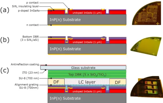
circular or square PDs with photosensitive areas ranging from 0.01 mm2 to 0.3 mm2. Figure 1(a) shows a schematic cross-section view as well as a top view image of the InP substrate at the end of the PD process. To fabricate these PDs, first, a dry etching of In0.53Ga0.47As layers down to the n-type InP contact layer is done to form mesas providing electrical
insulation between the different PD. Second, a 200 nm PECVD insulating layer of silicon nitride is deposited and etched to define electrical contact apertures at the surface of each mesa. Third, a 20 nm Ti and a 500 nm Au layers are evaporated and patterned by a liftoff process to form the top p-type contact when bottom n-type contact is ensured by the deposition of a 300 nm AuGe layer on the backside of the InP wafer.
Figure 1. Cross-section views and images of the tunable PD sample at different steps of the fabrication process, (a) after PD fabrication, (b) after deposition of the aSi/SiNx bottom DBR, (c) at the end of the process.
Then, a collective fabrication of microscopic LC cells monolithically integrated on each PD is done. These LC microcells act as tunable filters to operate at the end the device as a selective-wavelength PD. As shown in Figure 1(b), a first distributed Bragg reflector (DBR), consisting in 2.5 periods of amorphous silicon (aSi) and silicon nitride (SiNx) is
deposited by magnetron sputtering on the PD sample. This bottom DBR is added to the quarter-wave SiNx layer already
deposited by PECVD to finally form a DBR of 3 periods with a theoretical reflectivity of 97%. This DBR covers the main part of the sample except at the edges where an electrical access to the different PDs must be ensured (see image in Figure 1(b)). Then, on this bottom DBR, the surface has to be prepared for the future integration of LC microcells. Indeed, to benefit from the large refractive index variation offered by the LC, it is mandatory to orient the LC molecules in the same direction. This can be ensured by the creation of anisotropic surfaces which are put in contact with the LC material. Usually, for large and flat LCD display surfaces, it is done by a polyimide surface rubbing, which is a
well-known and effective method. However, this approach is not compatible with a micro-scale device process, especially when non-planar surface topography exists. In our fabrication process, this has been done by imprinting a sub-wavelength grating mold into a 700 nm thick SU-8 layer previously spin-coated on the DBR surface. After pattern transfer, the sub-wavelength grating has a period of 800 nm, a duty cycle of 50:50, and a depth in the range of [70-80 nm]. The details of this process are described elsewhere [12]. LC microcells are then defined by polymer walls made of an epoxy photosensitive film named DF-1005. This dry polymer film of 5 µm in thickness is applied to the surface of the sample by a soft thermal transfer[13]. Then this film is delimited to form DF walls and square shaped openings of 3.5×3.5 mm2 by a standard photolithography step (see image of Figure 1(c)). As illustrated in the cross-section view of the Figure 1(c), these microcells are then covered by a top DBR with a theoretical reflectivity of 95%, consisting of 5 x (SiO2/TiO2)
periods deposited on a glass substrate, previously coated with a 23 nm ITO transparent electrode having a sheet resistance of 100 Ω/□. This upper part of the device, covered by an antireflection layer at 1.55 µm, is then sealed to the top surfaces of the DF walls. The sealing is performed using 700 nm thick SU-8 layer spin-coated on the top DBR followed by an UV exposure through the UV-transparent SiO2/TiO2 DBR. Finally, the microcells are filled under
vacuum by a typical nematic LC (E7). This filling is achieved at a temperature higher than the nematic-isotropic transition (i.e. >70 °C) by using lateral apertures previously defined in the DF-1005 cells’ walls. At this stage, the fabrication of our device is completed and it can be used as a wavelength tunable PD.
3. RESULTS AND DISCUSSION
3.1 Tunable filter characterization
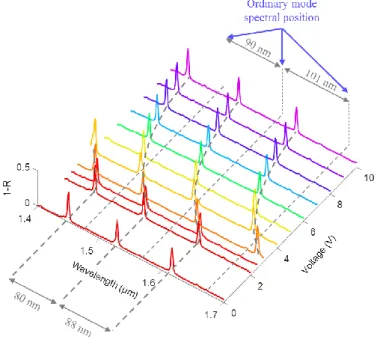
Before photocurrent measurements, the fabricated LC microcells integrated above the PDs have been characterized by a Fourier Transform InfraRed (FTIR) spectrometer. Here, the experiment consists in the polarization-resolved reflectivity measurements of the tunable filter. Figure 2 shows an overview of all the spectra recorded for an applied AC voltage at 2 kHz and different amplitudes comprised between 0 and 10V. The voltage is applied through the ITO and AuGe electrodes. These measurements were performed above the photosensitive area of a PD (380×380 μm2) which is larger than the area analyzed by the FTIR (150×150 μm2).
Figure 2. Evolution of reflectivity spectra (plotted as 1-R for improved clarity) measured by localized FTIR spectroscopy on a PD area for different AC voltages (2 kHz) varying from 0 to 10V in amplitude. The orientation of the polarizer was chosen to attenuate the “ordinary” modes.
In this experiment, the linear polarization of the incident light is parallel to the lines of the alignment grating. Thus, the resonant modes having this polarization are affected by the refractive index change when a voltage is applied on the LC
microcells. In the following, the modes with such a polarization will be referred as the “extraordinary modes” and those with a polarization perpendicular to the lines of the grating will be referred as the “ordinary modes”. In Figure 2, as the incident light is polarized to observe extraordinary modes only, ordinary modes are not visible but their spectral positions are indicated for information, as well as the corresponding values of free spectral ranges between successive modes (FSR). When a voltage higher than 2V is applied, the extraordinary modes are shifted towards shorter wavelengths, which is consistent with the fact that the extraordinary index (ne) decreases when the voltage is increased. The spectral
differences between ordinary and extraordinary modes have been studied by modeling the structure reflectivity using the transfer matrix method (TMM). The 90 and 101 nm spacings between the ordinary modes are correctly reproduced considering a LC thickness of 6.4 μm and an ordinary index (no) of 1.508. This thickness is higher than the expected one,
i.e. higher than the nominal thickness of the DF walls, and it can be explained by a SU-8 layer which is locally thicker than expected due to the spin-coating of this polymer on the non-planar topography of the InP sample after PD process. By tracking the extraordinary modes wavelength position with the voltage, the refractive index variation as a function of the applied voltage can be deduced with the TMM confrontation. The value deduced for ne is 1.689, close to that already
measured for this type of LC at 25 °C (ne = 1.697) [10],[12]
, confirming that the alignment of the LC molecules along the grating lines is efficient. This calculation leads to a refractive index variation of 0.15 for a voltage of 10V. This value is lower than the difference between ordinary and extraordinary indices (ne–n0 0.19) and it could be increased with the
use of higher voltage. However, as seen in figure 2, the wavelength shift efficiency with the voltage decreases beyond 7V, and a voltage of 10V is already sufficient to cover a large spectral window of 100 nm which is higher than the FSR of the filter. Regarding, the spectral width of the resonance modes, it was not measured from these FTIR spectra since the numerical aperture of the microscope objective used for focusing is not suitable for such measurements. These measurements have been performed from photocurrent experiments described in the next paragraph.
3.2 Tunable PD characterization
Photocurrent measurements were carried out using a tunable external cavity laser, delivering a continuous mode-hop-free tuning over 80 nm [1480 nm - 1560 nm] with a 5 MHz FWHM. The laser beam was focused with a lens of 40 mm focal length to form on the PD a spot with a diameter of 100 µm. This spot size is smaller than any PD area on the sample to ensure accurate efficiency calculation for each PD. Figure 3(a) shows the I-V curves without any LC voltage for a square PD (380 × 380 μm2) including the tunable filter whose characteristics have been described previously. As it can be seen in figure 3(a) where the excitation wavelength at 1527 nm is resonant with the LC filter, a photocurrent higher than 0.6 mA is detected without any LC voltage and when the PD is illuminated with an incident power of 1.4 mW. In the following, we have fixed the PD bias at 0V and measured the photocurrent amplitude as function of the applied LC voltage, and for different laser incident wavelengths (see figure 3(b)).
Figure 3 (a) I-V curves in the dark and under 1.4 mW illumination at 1527 nm for a 380 × 380 µm² PD without any LC voltage (b) Photocurrent for the same PD related to resonant extraordinary modes vs AC voltage (2 kHz) applied on the LC microcell for different lasing wavelengths fixed at an input power of 1.4 mW.
For the starting wavelength of 1527 nm, the photocurrent is almost constant at 0.62 mA over the LC voltage range [0V-2V], then it falls to almost the dark current value (around 1µA) from 2.5V to 7V, and finally presents a peak for a
voltage of 7.5V. As shown previously in figure 2, the LC extraordinary index remains constant over the [0V-2V] range, meaning that this high value of photocurrent corresponds to a match of the filter with the lasing wavelength of 1527 nm (central resonant mode at 0V in figure 2). The photocurrent peak at 7.5 V is related to the shift of the adjacent extraordinary mode previously measured by FTIR, initially located around 1600 nm (resonant mode on the right at 0V in figure 2) and found at 1527 nm for a LC voltage of 7V. As shown in figure 3(b), these measurements were performed for several wavelengths. For each wavelength, a photocurrent peak was detected for a particular LC voltage remaining below 7V, clearly demonstrating that this PD operates as a wavelength-selective PD over the whole available spectral characterization range (80 nm).
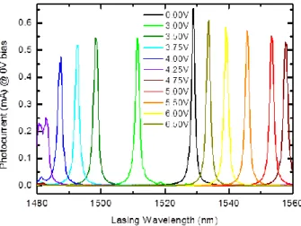
Figure 4. Photocurrent spectra of the resonant extraordinary modes measured for different AC voltage applied on the LC microcell as a function of the incident laser wavelength.
In order to evaluate the quality factor (Q-factor) of the resonant tunable filter and responsivity of the PD, photocurrent measurements with a continuous sweep on the incident laser wavelength and at a fixed LC voltage were also performed. (see figure 4). As it can be seen in this figure, without LC voltage, a resonant mode is detected slightly below 1530 nm with a maximum photocurrent of 0.65 mA for an illumination still set at 1.4 mW. As seen previously for a LC voltage higher than 2V, the resonant mode is blue-shifted. For a LC voltage of 4.5V, the resonant mode is outside the spectral window of the tunable laser, but from 4.75V a photocurrent can be detected again for wavelengths below 1560 nm. It corresponds to the extraordinary mode initially set around 1600 nm at 0V (see figure 2) which comes into the tuning band of the laser for LC voltage higher than 4.5V. Finally, for a voltage of 6.5V this resonant mode is found almost on the same spectral position as the one detected when no LC voltage is applied. Thus, the tuning range of the laser is fully covered for a driving voltage of 7V. Regarding the peak amplitude of the photocurrent, the values remain above 0.5 mA except in the band [1480 nm - 1490 nm] where a decrease in photocurrent is observed. This is related to the crossing between the ordinary and extraordinary modes (see Figure 2) leading to a coupling between them and a degradation of the Q factor for the tunable filter in this wavelength range. The same observation was made for the non-tunable ordinary mode located at 1482 nm by rotating the polarization of the laser by 90°. Regarding the responsivity, which is a key parameter for a PD, our results show that over a wide spectral range [1490 nm - 1560 nm], a responsivity comprised between 0.35 to 0.46 A/W is measured. A comparison with a reference PD was also made at the end of the PD process to evaluate the influence of the filter insertion on the device responsivity. In this case, the SiNx PECVD layer deposited on
the surface of the PD arrays plays the role of an antireflection coating to maximize the light absorbed by the PDs. The measured responsivities for these reference PDs are from 0.57 to 0.64 A/W in the same spectral range, which is consistent with values expected for such PDs integrating only a 1 µm thick In0.53Ga0.47As absorbing layer. In an
improved design, responsivities close to 0.8 and up to 1 A/W could be obtained with such tunable PDs by simply doubling the thickness of the absorbing layer[5]. Finally, the losses related to the integration of the tunable filter on the PD are estimated to be around 2 dB. As already mentioned above, these losses are not related to absorption from any materials within the microcavity. These 2 dB losses are mainly related to the maximal transmission of the filter at the
resonance, which is estimated to be around 80% due to a slight reflectivity mismatch between bottom DBR (97%) and top DBR (95%), and to residual absorption within the ITO layers located outside the microcavity.
4. CONCLUSION
In this work, we demonstrate tunable PDs consisting in LC microcells integrated on the surface of InGaAs PDs and acting as resonant microcavities. The tunable part of this device has been characterized by polarization-resolved reflectivity measurements with a FTIR spectrometer. A wavelength tuning higher than 100 nm at 1550 nm with a maximum driving voltage of 10V is achieved. Photodetection measurements were also performed thanks to a tunable laser, demonstrating that the PD is spectrally-tunable and can be swept from 1480 nm to 1560 nm. This spectral window was covered with a LC driving voltage of 7V only. The average responsivity over the major part of this spectral range is measured to be 0.4 A/W, corresponding to less than 2 dB of insertion loss. Q-factor of 103 and spectral linewidth of 0.15 nm have been measured, remaining almost constant over the considered spectral window [1490 nm - 1560 nm]. Some improvements could be achieved in the future by increasing the thickness of the absorbing layer, the Q-factor value and the FSR of the filter. Such improvements would allow for a significant increase in the PD responsivity, wavelength sensitivity and tunability. Considering these improvements, LC based approaches may become a relevant technology for the fabrication of tunable PDs in the visible and infrared wavelength range, especially if we consider that the presented technology can be easily adapted to any type of PDs. In addition, as the optical losses induced by LC are negligible, it may also be possible to consider using these LC microcells into a laser cavity to develop tunable emitters.
ACKNOWLEDGMENTS
The research leading to these results has received funding from Direction Générale de l'Armement (DGA) and Agence Nationale de la Recherche (ANR) through the followings programs: ANR-ASTRID HYPOCAMP (grant ANR-14-ASTR-0007-01), DGA-MRIS and Région Bretagne (grant ARED-VELOCE 8917) and grant ANR-15-CE19-0012 DOCT VCSEL. The authors acknowledge RENATECH (French Network of Major Technology Centers) for technological support. The tunable LC-PD technology was developed at LAAS, Nanorennes, and C2N (in collaboration with IMT Atlantique). The authors also acknowledge X. Lafosse from C2N for his technical support, R.-M. Sauvage (DGA/DS/MRIS) and H. Folliot (Institut FOTON) for fruitful discussions.
REFERENCES
[1] Qiao, P., Cook, K., Li, K., and Chang-Hasnain, C. J., “Wavelength-swept VCSELs”, IEEE J. Sel. Topics Quantum Electron. 23(6), 1700516 (2017).
[2] G. L. Christenson, A. T. T. D. Tran, Z. H. Zhu, Y. H. Lo, M. Hong, J. P. Mannaerts, and R. Bhat, “Long-Wavelength Resonant Vertical-Cavity LED/Photodetector with a 75-nm Tuning Range”, IEEE Photon. Technol. Lett. 9(6), 725–727 (1997).
[3] D. Zhou, M. Garrigues, J. L. Leclercq, J. Peng, and P. Viktorovitch, “A Phase-Matching and Pseudoresonance-Enhanced Design for Tunable Micromachined Photodetectors”, IEEE Photon. Technol. Lett. 15(10), 1443–1445 (2003).
[4] H. Halbritter, F. Riemenschneider, S. Syguda, C. Dhanavantri, M. Strassner, A. Tarraf, B.R. Singh, I. Sagnes and P. Meissner, “Tunable and wavelength selective PIN photodiode”, Electon. Lett. 40(6), 388–390 (2004). [5] J. Cesar, S. Paul, M. T. Haidar, B. Corbett, A. Chipouline, and F. Küppers, “Surface Micromachined
MEMS-Tunable PIN-Photodiodes around 1550-nm”, in Conference on Lasers and Electro-Optics, OSA Technical Digest (online) (Optical Society of America, 2017), paper STu1N.7.
[6] T. H. Wood, C. A. Burrus, A. H. Gnauck, J. M. Wiesenfeld, D. A. B. Miller, D. S. Chemla, and T. C. Damen, “Wavelength-selective voltage-tunable photodetector made from multiple quantum wells”, Appl. Phys. Lett. 47(3), 190–192 (1985).
[7] Y. Shi, J. H. Zhao, J. Sarathy, G. H. Olsen, and H. Lee, “Tunable resonant cavity enhanced photodetectors with GaInAsSb/AlGaAsSb multiple quantum well structure grown by molecular beam epitaxy”, Electron. Lett. 33(17), 1498–1499 (1997).
[8] W. Wang, X. Ren, H. Huang, X. Wang, H. Cui, A. Miao, Y. Li, and Y. Huang, “Tunable Photodetector Based on GaAs/InP Wafer Bonding”, IEEE Electron Device Letters 27(10), 827–829 (2006).
[9] J. Lv, H. Huang, X. Ren, A. Miao, Y. Li, H. Song, Q. Wang, Y. Huang, and S. Cai, “Monothically Integrated Long-Wavelength Tunable Photodetector”, IEEE J. Of lightwave Technol. 26(3), 338–342 (2008).
[10] K. Hirabayashi, H. Tsuda, and T. Kurokawa, “Tunable Liquid-Crystal Fabry-Perot Interferometer Filter for Wavelength-Division Multiplexing Communication Systems,” IEEE J. of Lightwave Technol. 11(12), 2033– 2043 (1993).
[11] W. Vogel and M. Berroth, “Tunable liquid crystal Fabry-Perot filters,” Proc. SPIE 4944 (2003).
[12] B. Sadani, B. Boisnard, X. Lafosse, T. Camps, J.-B. Doucet, E. Daran, C. Paranthoen, C. Levallois, L. Dupont, S. Bouchoule, and V. Bardinal, “Liquid-Crystal alignment by a nanoimprinted grating for wafer-scale fabrication of tunable devices,” IEEE Photon. Technol. Lett. (Early access: DOI 10.1109/LPT.2018.2849641) [13] S. Abada, L. Salvi, R. Courson, E. Daran, B. Reig, J.B. Doucet, T. Camps, and V. Bardinal, “Comparison of
lamination and soft thermal printing of dry thick photoresist films for the uniform fabrication of polymer MOEMS on small-sized samples,” J. Micromech. Microeng. 27, 055018, (2017).