This is an author-deposited version published in:
http://oatao.univ-toulouse.fr/
Eprints ID: 2835
To cite this document:
WANE, Sidina. BAJON, Damienne. Characterisation and
macro-modeling of patterned micronic and nano-scale dummy metal-fills in
integrated circuits. In: 2009 International Microwaves Symposium, 07-12 June
2009, Boston, USA.
Any correspondence concerning this service should be sent to the repository
administrator:
[email protected]
Characterisation and Macro-modeling of Patterned
Micronic and Nano-Scale Dummy Metal-Fills in
Integrated Circuits
Sidina Wane
1and Damienne Bajon
21
NXP-Semiconductors Campus-EffiScience, Caen– France Email: [email protected]
2ISAE-Toulouse Université, 10 avenue Edouard Belin 31055, Toulouse-France, Email: [email protected]
Abstract— In this paper, a wideband characterization and
macro-modeling of patterned micronic and nano-scale dummy metal-fills is presented. Impacts of patterned dummy metal-fill topologies including square, cross, vertical and horizontal shaped arrays on electrical performances (isolation/coupling, attenuation, guiding properties, etc…) are investigated. The validity of the proposed macro-modeling methodology is demonstrated by comparison with high frequency measurements of dedicated carrier structures including on-chip interconnects and RF inductive loops. An original extraction approach, based on local ground concept, is proposed to capture high frequency behaviour of dummy metal-fill in physics-based compact broadband SPICE model. The RLC parameters are accurately derived using fully scalable closed-form semi-analytical expressions.
Keywords— Patterned Metal-Fills, Broadband Scalable Macromodeling, Wideband SPICE model extraction.
I.INTRODUCTION
In modern integrated circuits, operating at increasingly higher frequencies, multi-physics design constraints resulting from process technology requirements can impact systems electrical performances. Among such constraints is the significant number of patterned dummy metal-fills introduced to adjust the metal density for controlled thichness of inter-level dielectrics using chemical-mechanical-polishing (CMP) techniques. In [1] challenges of inter-level dielectric thichness uniformity are discussed in the context of ASIC applications. CMP techniques suffer from layout pattern sensitivity which causes certain regions of a chip to have thinner dielectric layers than other parts. Such effects, when coupled with statistical variations in process parameters spread can jeopardize circuit functionality. The resulting inter-level dielectric thickness variations in combination with potential effects of patterned dummy metal-fills require efficient characterization and modeling techniques to be properly taken into account.
The multi-scale characteristics resulting from the discrepancy between the dummy metal-fill dimensions compared to the wavelength of circuits operating frequencies involve high complexities and memory requirement for available full-wave electromagnetic simulators and quasi-static extraction tools. This makes their simulation extremely challenging. Therefore, impact of dummy metal-fill at chip
scale is not yet well understood, hence the need for global characterization and macro-modeling approaches.
In previous research work, some potential benefits and limitations of floating/grounded dummy metal-fill on integrated on-chip interconnects have been discussed. In [2] metal-fills are seen reducing IR-drop and electromigration effects on power delivery network, while in [3] influence of patterned ground-shield on high-frequency eddy-current losses for RF inductors are studied from full-wave analysis. In [4] RF isolation enhancement using dummy metal-fills based on capacitive loading is discussed. Most of previous investigations on dummy metal-fills have mainly focused on capacitive type of effects, with very limited analysis of inductive and resistive type of effects. While, at low frequency, capacitive, inductive and resistive effects due to dummy metal-fills can be assumed independent, they are coupled at high frequencies and require global analysis.
In this paper a global macro-modeling approach based on broadband analysis and characterization (beyond 100GHz) of patterned dummy metal-fills is proposed. Impact of patterned dummy metal-fill topologies including square, cross, vertical and horizontal shaped arrays on electrical performances (isolation/coupling, guiding properties, etc…) are investigated. The proposed approach, in its ability to accurately capture the wideband characteristics of metal-fills attributes in physics-based equivalent circuit models, opens the door for unification of micronic metal-fills macro-modeling and meta-material analysis. The limits of classical homogenisation techniques are discussed based on physical considerations. The validity of the methodology is demonstrated by comparison with high frequency measurement for a wide-range of carrier structures (CPW Transmission Lines, integrated loops/RF-inductors) designed with different metal-fill topologies.
II.EFFECTS OF PATTERNED DUMMY METAL-FILLS ON ON-CHIP
TRANSMISSION LINES
A) Description of Characterization Structures
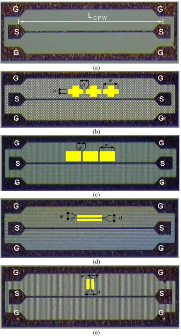
To investigate effects of patterned dummy metal-fills on on-chip transmission lines five different structures have been designed, fabricated and measured using a Network Analyzer (reference E8364B_HP4141) and a coplanar G-S-G probes in
the frequency band 100MHz -110GHz. The microphotographs of the designed structures are shown in Fig.1 (a), (b), (c), (d), (e). Fig.1 (a) represents the reference CPW line without tiling. In the other structures a metal-fill patterning layer underneath the CPW line (0.5 μm below) is introduced with different tiling topologies. Fig.2 (b) and Fig.2(c) respectively represent CPW lines with cross and square shaped tiling. The Fig.1 (d) and Fig.1(e) refer to horizontal (parallel) and vertical (orthogonal) tiling. S G G S G G LC P W S G G S G G S G G S G G S G G S G G LC P W (a) S G G S G G S G G S G G S G G S G G w h d (b) S G G S G G S G G S G G S G G S G G w d (c) S G G S G G w d S G G S G G S G G S G G S G G S G G w d (d) S G G S G G S G G S G G S G G S G G w d (e)
Fig 1. Microphotographs of designed CPW on-chip transmission lines without tiling (a), with different metal-fill patterning: Cross-tiling (b), Square-tiling (c), Horizontal-tiling (d) and Vertical-tiling (e).
B) Effects of Dummy Metal-Fill on Transmission-Lines Primary Parameters
In order to evaluate effects of dummy metal-fills on the primary parameters ((Propagation Constant, Characteristic Impedance and Effective Permittivity) of the designed CPW transmission line structures the associated Y-matrix in (1) is
extracted from S-parameters where θ =γL is the electrical length,γ =α+ jβ being the propagation constant:
[ ]
[ ]
[ ]
[ ]
¸¸¹· ¨¨© § − − = − − − θ θ θ θ coth sinh sinh coth 1 1 1 C Z Y (1)The propagation constant is classically extracted from chain-matrix ABCD given by:
[
]
=§¨¨© ·¸¸¹=¨¨©§ −[ ]
[ ]
[ ]
[ ]
·¸¸¹ θ θ θ θ cosh sinh sinh cosh 1 C C Z Z D C B A ABCD (2)in taking the inverse of hyperbolic functions sinh or cosh. Due to high inaccuracies that result from the numerical evaluation of inverse hyperbolic functions, an alternative extraction approach is introduced for high frequency applications. In Fig.2, such numerical inaccuracies are illustrated for the calculation of a well-known identity cosh²(x)-sinh²(x)=1, using Matlab. The existence of an instability region where the identity is not fulfilled for numerical reasons is demonstrated. So, high frequency applications extraction of transmission lines primary parameters using hyperbolic functions, without precautions, can lead to inaccurate results.
Fig.2. Illustration of numerical inaccuracies in computing the classical identity cosh²(x)-sinh²(x)=1.
To circumvent the numerical problems illustrated in Fig.2, the introduced methodology extracts the transmission line primary parameters directly giving compact closed-form expressions with strong numerical stability. From the complex eigen-values of the chain matrix given in (2) expressed in terms of S-parameters, the broadband complex effective permittivityε : eff
(
)
(
(
)
)
i eff r eff eff γ jβ α jβ jβ ε jε ε = = + 2 = + 0 2 0 (3)whereβ is the wave-number in free-space and such that 0
0 =
i eff
ε indicates stop-band in band-gap structures.
The attenuation constant α can be derived using the following closed-form expression:
(
)(
)(
)(
)
[
]
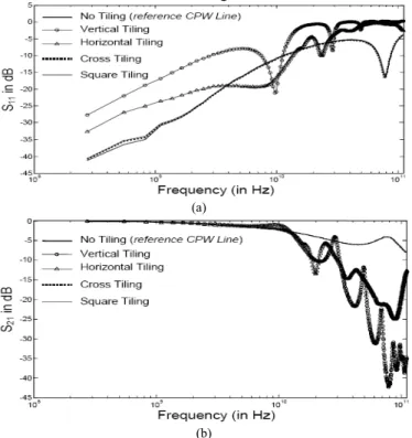
¸¸ ¸ ¹ · ¨¨ ¨ © § Δ − Δ Δ + Δ − Δ + Δ − ± Δ Δ − − = − = − + − − + + − + 12 0 1 1 1 1 1 log 1 2 L k r eff eff ε ε α (4) with Δ+ =S11+S12 and Δ−=S11−S12. 172The transmission S12 parameters of the five structures in
Fig.1 show in Fig. 4(a) significant effect of vertical and horizontal tiling. The wave-numberβ extracted from (3) and (4) as β = k εeff +εeffr
2
0 and the attenuation (4) can be
easily extracted from measurement. Fig. 4(a)-(b) show measured S11 and S21 against frequency for the different
patterned metal-fills in Fig.1. Flat parts observed in stepped wave-number variations, associated to high attenuation levels, denote periodic strong decay in group velocity or band gaps for the structure with vertical tiling.
(a)
(b)
Fig 3. Measured S11 (a) and S21(b) parameters of the different patterned metal-fills in Fig.1 (no-tiling, cross-tiling, square-tiling,
horizontal-tiling and vertical-tiling ).
B) Derivation of Broadband Scalable Physics-based SPICE Macromodels
A compact scalable broadband equivalent circuit model is derived to capture the behavior of the CPW transmission line including the effects of the patterned metal-fills, without any limitation with respect to frequency. The proposed extraction methodology [5] uses Mittag-Leffler expansion of hyperbolic functions. In the lossless case without loss of generality the following Mittag-Leffler expansions can be derived to extract wideband SPICE models for the input admittance of transmission structures with open and short conditions at one of the access ports.
[ ]
(
( )
)
[ ]
° ° ¯ ° ° ® ¸ ¸ ¹ · ¨ ¨ © § − ¸ ¹ · ¨ © § − = = = »¼ º «¬ ª + − − = − = =¦
¦
∞ = − − − ∞ = − − − 1 1 2 2 2 1 1 1 1 2 2 1 1 2 1 2 tan 1 2 1 cot 1 k C C o Short k C C e Open k jZ jZ Z Y k jZ jZ Z Yθ
π
θ
θ
π
θ
θ
θ
θ
(5)Pole expansion of the input admittances given in relations (5) gives a straightforward derivation of SPICE equivalent circuit models. In the lossy case, the equivalent circuit architecture in Fig.4 can be considered for casting the admittance parameters in canonical RLC branches. Classical Π and/or T equivalent circuit representations are generally based on global ground reference assumptions (signal-input and signal-output in Fig.4 being referenced to same ground node). The proposed Trellis architecture topology introduced in [5] circumvents such limitations. Extracted circuit elements from structures defined in Fig 1 are given in TABLE I where high resistive values are closely related to observed band gaps.
Fig 4. Scalable Broadband equivalent circuit macro-model accounting for floating ground references.
TABLE I:EFFECTS OF TILING ON EXTRACTED BROADBAND EQUIVALENT
CIRCUIT MODEL PARAMETERS
Extracted Broadband Equivalent Circuit Model Parameters (for k=1 in Fig.4)
Measured Options L0 (nH) C0k (fF) CSk (fF) Rok (Ω) Rek (Ω) RLF (Ω) Cross Tile 0.23 21.3 5.34 65 15.84 0.37 Vertical Tile 0.148 290 72.6 10-4 >10+4 >10+4 Horizontal Tile 0.135 28.6 7.15 >10+4 163 >10+4 Square Tile 0.228 21.02 5.25 69 15.84 0.35 No-Tiling 0.23 20.3 5.09 65 16.85 0.35
The reactive elements in TABLE I (inductive and capacitive parameters) in the equivalent circuit of Fig 4 are given by the following closed-form expressions requiring only the two complex valued parameters Zc and εeff .
( )
(
)
(
)
1 1 2 1 1 0 1 1 2 1 1 2 , 2 1 2 2 , 2 , , − − − − − ¸¹ · ¨© § = ¸ ¹ · ¨ © § − = = = = = = r eff CPW c C k C Sk LF sk ok C L v k Z C Z k C L L L L L Z L ε ω πω πω πωwhere
v
cis the light velocity in free space.III.EFFECTS OF PATTERNED DUMMY METAL-FILLS ON LOOPS AND RF-INDUCTORS.
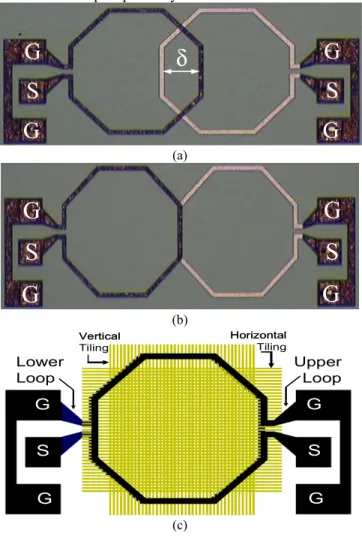
Different coupled inductive loops are designed, measured (up to 110 GHz) and modeled to evaluate effects of dummy metal-fills on isolation performances. The inductive loops are on two different layers separated by an intermediate tiling layer where the metal-fills are drawn. Fig. 5(a) and (b) show the
microphotographs of the coupled inductive loops with δ=20% and δ=0% overlap respectively.
δ
G
S
G
G
S
G
(a)G
S
G
G
S
G
(b) G G S G G S LowerLoop Upper Loop
Vertical Tiling Horizontal Tiling G G S G G S Lower
Loop Upper Loop
Vertical Tiling
Horizontal Tiling
(c)
Fig 5. Microphotographs of designed on-chip inductive loops with different overlap (δ in percentage of loop-area): option (a) is for δ=20%, option (b) is for δ=0%. Option (c) represent a top-view of the coupled loops with Vertical+Horizontal metal-fill for δ=100%.
Fig.6 (a) shows the influence of overlap between inductive loops on measured isolation performances, where a non-monotic behavior is observed, a maximum coupling been obtained for a δ=100% overlap. In Fig.6 (b), the effects of different tiling topologies (square, horizontal, vertical, horizontal + vertical) on coupling between the loops is presented. Micronic squared-shaped metal-fill are seen to have limited impact on coupling between the loops while vertical and horizontal wires tiling lead to non-negligible influences. Resonant effects are observed for the vertical and horizontal tiling topologies, the location of the resonant frequencies can be accurately predicted based on the topology of the considered metal-fill elements and the previously described primary parameter extraction in section II.A.
The particular attributes of the coupled loops probing in Fig.5 regarding local grounding references is used to assess the robustness of the proposed extraction methodology.
(a) 10 20 30 40 50 60 70 80 90 100 110 120 -25 -20 -15 -10 -5 0 Frequency (in GHz) S21 ( in dB ) Square-shaped Metal-Fill Horizontal Wires Metal-Fill Vertical Wires Metal-Fill
Vertical+Horizontal Wires Metal-Fill
(b)
Fig 6. Influence of overlap between inductive loops on measured isolation performances (a), effects of metal-fill topology shapes (square, horizontal, vertival, horizontal+vertical) on simulated EM coupling (b).
IV.CONCLUSION
A wideband characterization and macro-modeling of patterned micronic and nano-scale dummy metal-fills has been presented. Impact of patterned dummy metal-fills arrays on electrical performances has been investigated. The validity of the proposed macro-modeling methodology is demonstrated by comparison with high frequency measurement of dedicated carrier structures including on-chip interconnects and RF inductive loops. The proposed extraction approach captures high frequency behaviour of dummy metal-fills in compact broadband SPICE models accounting for local ground references not possible with classical Π and/or T equivalent circuit representations. The proposed methodology opens the door for unification of micronic/nanoscale metal-fills and meta-material analysis.
REFERENCES
[1] B. Stine, D. Boning, et al., “The physical and electrical effects of metal-fill patterning practices for oxide chemical mechanical polishing processes,” IEEE Trans. Electron Devices, vol. 45, p. 665, Mar., 1998. [2] K.-S. Leung, “SPIDER: Simultaneous Post-Layout IRDrop and Metal
Density Enhancement with Redundant Fill,” Int. Conf. on Computer-Aided Design, ICCAD- 2005, pp. 33 – 38, Nov. 2005.
[3] S.Wane and D.Bajon, “Full-Wave Analysis of Inhomogeneous Deep-Trench Isolation Patterning for Substrate Coupling Reduction and Q-Factor Improvement, ”IEEE Trans. Microwave Theory Tech., vol. 54, no.12, Part 2, pp. 4397 – 4411, Dec. 2006.
[4] S. G. Gaskill, V.S. Shilimkar, and A. Weisshaar, “Isolation Enhancement in Integrated Circuits Using Dummy Metal Fill,” IEEE RFIC Symp. June 2008, pp.483 – 486.
[5] S.Wane, D.Bajon, P.Russer, Y. Kuznetsov, A.Baev, N. Fichtner and Uwe Siart, “Broadband Equivalent Circuit Derivation for Multi- Port Circuits Based on Eigen-State Formulation”, accepted for IEEE-IMS 2009.