O
pen
A
rchive
T
oulouse
A
rchive
O
uverte (
OATAO
)
OATAO is an open access repository that collects the work of Toulouse researchers and
makes it freely available over the web where possible.
This is an author deposited version published in: http://oatao.univ-toulouse.fr/
Eprints ID: 3344
To link to this article: DOI: 10.1109/ICECS.2009.5410825
URL: http://dx.doi.org/10.1109/ICECS.2009.5410825
To cite this document: MARTIN-GONTHIER, Philippe, MAGNAN, Pierre. RTS Noise
Impact in CMOS Image Sensors Readout Circuit. In : 16th IEEE International
Conference on Electronics, Circuits, and Systems, 2009, ICECS 2009, Hammamet,
Tunisia, 13-16 December 2009. Piscataway NJ : IEEE, 2010, pp. 928-931. ISBN
978-1-4244-5090-9
Any correspondence concerning this service should be sent to the repository administrator:
Abstract—CMOS image sensors are nowadays widely used in
imaging applications even for high end applications. This is really possible thanks to a reduction of noise obtained, among others, by Correlated Double Sampling (CDS) readout. Random Telegraph Signal (RTS) noise has thus become an issue for low light level applications especially in the context of downscaling transistor dimension. This paper describes the analysis of in-pixel source follower transistor RTS noise filtering by CDS circuit. The measurement of a non Gaussian distribution with a positive skew of image sensor output noise is analysed and dimension (W and L) impact of the in-pixel source follower is analysed.
Index Terms—Image sensors, RTS noise, low frequency noise,
Correlated Double Sampling
I. INTRODUCTION
CMOS image sensors are nowadays extensively used in commercial applications. CMOS standard processes, which are developed for digital and mixed signal applications, are really attractive particularly because of their low power consumption, applicability for on-chip signal processing and large availability. Several ways have been explored to improve image sensor performances to a very high level and performances have been significantly enhanced with the use of CIS (CMOS Image Sensor) processes [1] [2] [3].
Image sensors performances are described by key parameters which are Quantum Efficiency (QE), Conversion gain (CG), Dark Current (DC), Noise, Full Well Capacity (FWC), Photo-Response and Dark Signal Non-Uniformities (respectively PRNU and DSNU) and Modulation Transfer Function (MTF). Noise impacts strongly the Dynamic Range. In order to maximize the pixel photosensitive area, the use of aggressive technologies and small MOS transistors in the pixel are required. That leads to an increase of MOS transistor low frequency noise impact. The use of Correlated Double Sampling (CDS) circuits and readout mode allow elimination of photodiode reset noise (KTC noise) which is usually the major noise contributor. At the same time, it reveals the Random Telegraph Signal (RTS) noise impact of the in-pixel source follower transistor. This RTS noise becomes an issue for the low light sensitivity [4].
In the first part of section II, a description of RTS noise and its parameters is done. Then, standard CMOS image sensor architecture with CDS readout circuit is given. The last part of section II illustrates impact of RTS noise of the in-pixel source follower transistor on the sensor output noise response. Section III shows the impact of CDS parameters, such as CDS period and sampling time, on RTS noise filtering by CDS circuit. That leads to an accurate model in order to predict impact of CDS parameters changes.
Section IV is devoted to the image sensor output noise histogram analysis. The effects of in-pixel source follower transistor size changes on RTS noise are also studied.
Section V presents a conclusion and perspectives of this work.
II. RTS NOISE IN CMOSIMAGE SENSOR
A. RTS noise modeling
Low frequency noise in large area devices, showing most of the time a 1/f Power Spectral Density, are well characterized by the use of appropriate models known as McWhorter model [5] dealing with carrier number fluctuation, Hooge model [6] dealing with mobility fluctuation or the unified model [7] dealing with carrier number fluctuation inducing mobility fluctuation.
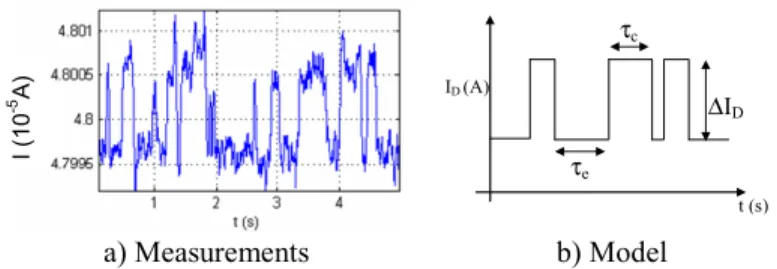
For small devices, carrier number becomes small and impact of trapping/detrapping events, caused by an individual interface defects at Si/SiO2 interface, shows discrete drain current fluctuations. Fig. 1a illustrates measurement of this current fluctuation caused by one defect at Si/SiO2 interface for a small MOSFET.
I ( 10 -5 A ) t (s) ID (A) τc τe ΔID a) Measurements b) Model
Fig. 1: RTS noise example coming from one defect at Si/SiO2 interface of a small MOSFET
As can be seen in Fig. 1-b, three parameters can describe a two levels RTS noise: τe, the average carrier emission time, τc,
the average carrier capture time and ΔID, the drain current
RTS amplitude. χ σ τ 0 T I e D kT E c B Δ = (1) η σ τ 0 2 T e kT E E e CT B+Δ Δ = (2) ⎟⎟ ⎠ ⎞ ⎜⎜ ⎝ ⎛ − = Δ OX t OX D m D D t x WLC q I g I I 1 . . η (3)
Equations (1), (2) and (3), [8] and [9] depict these
parameters where ΔEB is the trap energy level, ΔECT is the
difference between energy levels of conduction band and trap,
σ0 is the trap section, xT is the distance between trap and
Si/SiO2 interface, tOX is the gate oxide thickness, T is the
temperature, k is the Boltzman constant, ID is the MOSFET
drain current, gm is the MOSFET transconductance, W and L
RTS Noise Impact in CMOS Image Sensors Readout Circuit
P. Martin-Gonthier, P. Magnan
Université de Toulouse, ISAE, 10 avenue E. Belin, 31055, Toulouse, France
[email protected]
are the MOSFET dimensions and η and χ are fabrication process constants.
The probability of trap occupancy (PTO) [10], shown by equation (4), can be deduced from equations (1) and (2).
t c e e
K
e
e ct
P
). 1 1 (.
)
(
τ ττ
τ
τ
− ++
+
=
(4)This equation (4) depicts the trap probability to be occupied at every moment. K depends on the initial condition. In steady state, the PTO becomes τe/(τe +τc).
Due to downscaling, RTS noise becomes an issue in CMOS image sensor readout circuits [11]. In order to model the impact of RTS noise on CMOS image sensors noise response, a detailed description of sensor architecture and readout sequence is done in the next part of this section.
B. CMOS image sensor architecture and readout sequence
A common CMOS image sensor readout circuit architecture is shown in Fig. 2. It is composed of:
• a photo-element : a photodiode, or a pinned photodiode associated with a transfer gate
• a reset switch allowing to reset the photo-element or the readout node
• an in-pixel source follower which drives the signal from pixel to column readout circuit
• a double sample and hold circuit for reference and integrated signal level
• an output stage allowing to drive the signal off chip or on chip for additional processing
IN-PIXEL SOURCE FOLLOWER PHOTOELEMENT PIXEL COLUMN BUS Pinned photodiode TG RST RS SF Readout node VREF COLUMN READOUT CIRCUIT RST ROW
SELECTION SHR SELECTION COLUMN VDD
RESET CIRCUIT
SAMPLE AND HOLD OUTPUT
STAGE A1 A2 CSHR VSIG SHS COLUMN SELECTION OUTPUT STAGE A2 CSHS
SAMPLE AND HOLD
Fig. 2: Common readout circuit architecture of a CMOS image sensor
For a pinned photodiode pixel, before the beginning of the integration time, the photodiode is emptied by charge transfer mechanism. Before the end of integration time, the readout node is reset by the reset MOSFET (command signal RST). This level, called reference, is sampled and held (command signal SHR) in the column readout circuit in the reference channel via the in-pixel source follower (SF) and the row selection (RS) transistor. At the end of the integration time, charges integrated in the photodiode are transferred (command signal TG) in the readout node. The voltage level corresponding to the integrated charges is sampled and held (command signal SHS) in the column readout circuit of the signal channel. Video signal voltage level results from the subtraction of the two samples (reference and signal). Thus,
CDS readout is done by this sequence. CDS readout allows [12]:
• to eliminate reset noise coming from the reset of the readout node (capacitance) due to RST transistor thermal noise
• to remove pixel to pixel Fixed Pattern Noise (FPN) due to in-pixel source follower offset dispersion from pixel to pixel
• to reduce low frequency noise by CDS high pass filtering function.
Equation (5) shows the time domain operation carried out by the CDS circuit and the chronogram depicted in Fig. 3.
[
(
)
(
)
]
).
(
)
(
IN CDS St
V
t
t
t
T
V
=
δ
−
δ
−
(5) SHR SHS VS VIN _ + t t SHS SHR TCDS TP TS a) Synoptic b) chronogramFig. 3: Synoptic and chronogram of CDS system
C. RTS noise impact on CMOS image sensor noise response
As can be seen in §B, CDS principle requires two samples which are provided by the in-pixel source follower transistor. If this transistor produces significant RTS noise, the pixel voltage response at the image sensor output shows different levels areas as depicted in Fig. 4 [13]. SHR and SHS are the two samples taken at different moment. This measurement result comes from an image sensor test designed in UMC CIS 0.35µm technology using 3T photodiode (described in section IV) and readout with a special sequence allowing CDS readout. TIME (s) SHR SHS SHR SHR SHS SHS PIXEL OUTPUT SIGNAL BEFORE CDS (V) SHR SHS
Fig. 4: Image sensor output noise response subject to significant RTS noise of in-pixel source follower transistor
For a two level RTS noise, three states can be seen. These three states correspond to the four ways that the samples are affected by RTS noise.
The histogram shown in Fig. 5 presents the noise distribution at the sensor output of 4095 pixels (part of the imager). This distribution shows a non-gaussian shape with a positive skew. This positive skew comes from the significant
RTS noise of the in-pixel source follower impacting on the image sensor output noise response [11].
The next sections deal firstly with CDS parameters impact on temporal pixel histogram. Secondly, the pixel noise distribution, affected by the RTS noise, is analysed with regard to the in-pixel source follower dimensions impact.
Fig. 5: Pixel output noise distribution at the sensor output
III. CDS PARAMETERS IMPACT ON RTS NOISE RESPONSE
This section presents the histogram measurement results on one pixel which is subject to in-pixel source follower RTS noise for different CDS periods and different sampling times. This sampling time and CDS period are denoted in Fig. 3 as,
respectively TS and TCDS. Before, after and between SHR and
SHS, the in-pixel source follower is turned off by the row selection transistor (RS in Fig. 2). Fig. 6 illustrates the voltage output histogram of one pixel and its associated probability
trap occupancy (PTO) for different values of TCDS and
TS=200ns. The PTO, denoted P1 and P2, are respectively
taken at the end of sampling time SHR and SHS. The left peak value of the histogram is P2)*P1, the right peak value is (1-P1)*P2 and finally the center peak value is (1-P1)*(1-P2)+P1*P2 [13].
PIXEL L44 C94 TS=200ns RS OFF
PIXEL OUTPUT SIGNAL (V)
FRE Q UE N C Y PIXEL L44 C94 TS=200ns RS OFF
PIXEL OUTPUT SIGNAL (V)
FRE Q UE N C Y TCDS(µs) PT O PIXEL L44 C94 TS=200ns RS OFF TCDS(µs) PT O PIXEL L44 C94 TS=200ns RS OFF
Fig. 6: Voltage output histogram of a pixel and its associated probability trap occupancy for TS=200ns
As can be seen, the right peak value stays constant, and the left and center peak values move. These changes can be explained by the analysis of the probability trap occupancy. Fig. 7 gives the temporal evolution of P1 and P2 with the help
of equation (4). As the TCDS increases, P1 decreases between
the two samples and P2 value also decreases (P2 does not
reach the steady state in this case). Thus, when the CDS period is decreasing, the P2 value is increasing leading mainly to a reduction of the left peak and an increase of the center peak.
t P(t) SHS SHR P1 P2 P2’ P2’’ TCDS1 TCDS2 T CDS3
Fig. 7: P1 and P2 temporal evolution during CDS sequence
This analysis is confirmed by the same measurements done
with TS=1µs. The same evolution model of PTO can be used
to explain histogram and PTO evolution.
PIXEL OUTPUT SIGNAL (V)
FR E Q UE N C Y PIXEL L44 C94 TS=1µs RS OFF
PIXEL OUTPUT SIGNAL (V)
FR E Q UE N C Y PIXEL L44 C94 TS=1µs RS OFF TCDS(µs) PT O PIXEL L44 C94 TS=1µs RS OFF TCDS(µs) PT O PIXEL L44 C94 TS=1µs RS OFF
Fig. 8 : Voltage output histogram of a pixel and its associated probability trap occupancy for TS=1µs
Impact of CDS parameters on RTS noise response depends
on RTS temporal parameters value τe and τc. However, as
CDS acts as a high pass filter and RTS noise is a low frequency noise, a decrease of CDS period and sampling time leads to a decrease of RTS noise.
IV. PIXEL NOISE DISTRIBUTION ANALYSIS IN FUNCTION OF THE
IN-PIXEL SOURCE FOLLOWER DIMENSION
Fig. 5, shown previously, depicts a pixel output noise distribution of 4095 pixels (part of the image sensor). This distribution is non-gaussian and have a significant positive skew which is a feature of a RTS noise impact [4].
Test image sensors were designed with various in-pixel source follower transistor dimensions in order to see impact on RTS noise. One of these test vehicles is illustrated in Fig. 9. As can be seen, each test vehicle is composed of four zones (pixel areas) with different W/L of the in-pixel source follower transistor. Histogram of pixel output noise for W=1.5µm and L variation of the in-pixel source follower transistor is shown in Fig. 10.
Two facts can be noted: 1) peak value change with W/L change which is in line with thermal noise impact of in-pixel source follower transistor 2) Distribution skews are not the same. Log scale is preferred to show the different slopes of the skew. These slopes increase as L dimension increases which means there are less noisy pixels (RTS noise amplitude decrease).
Fig. 10 : Histogram (log scale) of pixel output noise for W=1.5µm and L variation of in-pixel source follower transistor
Same measurements were done but with a fixed L (0.8µm) and a W variation. These measurement results are presented in Fig. 11. Once again, different slopes on the distribution skew are seen. Slopes increase as W dimension increases.
Fig. 11 : Histogram (log scale) of pixel output noise for L=0.8µm and W variations of in-pixel source follower transistor
In both cases, L and W variations, it can be noticed that noise mean value moves which is due to thermal noise change on source follower transistor.
Martin and al [14] show RTS noise dependence only with L
dimension. Their work was based on single transistors. Our results, obtained from imagers, demonstrate RTS noise dependence with the both dimensions W and L, as already obtained by Lahav and al [15].
V. CONCLUSION AND FUTURE WORK
This work shows the impact of the CDS parameters on the RTS noise response. The ways to optimise CDS filtering with regard to RTS noise are given. Measurement results show also a strong dependence of the RTS noise to L and W dimensions of the in-pixel source follower transistor. Increasing L and W decreases the noisy pixel number impacted by RTS noise. This work gives several perspectives in order to understand the RTS noise mechanism. Future works will focus on the RTS noise distribution which can be deduced of pixel output noise histogram. This RTS noise distribution will help us to find a model for W and L variations.
REFERENCES
[1] M. Furumiya and al, « High sensitivity and No-Crosstalk pixel technology for embedded CMOS Image Sensor », Electron Devices, IEEE Transactions on, Vol. 48, NO. 10, October 2001.
[2] H. Ihara and al, « A 3.7 x 3.7 µm2 square pixel CMOS image sensor for
digital still camera application », in ISSCC Tech. Dig., Feb. 1998, pp. 182-183.
[3] O.-B. Kwon and al, « An improved digital CMOS imager », in Proc. IEEE Workshop Charge-Coupled Devices and Advanced Image Sensors, June 1999, pp. 144-147.
[4] K. Findlater , J.M Vaillant, D.J. Baxter, C. Augier, D. Herault, R.K. Henderson, J.E.D. Hurwitz, L.A. Grant and J-M Volle, “ Source follower noise limitations in CMOS active pixel Sensors”, Detectors and Associated Signal Processing. Proceedings of the SPIE, Volume 5251, pp. 187-195 (2004).
[5] A. L. McWhorter, 1/f noise and germanium surface properties. Semiconductor H. Surface Physics (1957).
[6] F. N. Hooge, 1/f Noise is no surface effect. Physics Letters (1969). [7] Hung, K.; Ko, P.; Hu, C. & Cheng, Y. “A unified model for the flicker
noise in metal-oxide-semiconductor field-effect transistors”, Electron Devices, IEEE Transactions on, 1990, 37, 654-665.
[8] M.J. Kirton et al., “Noise in Solid-State Microstructures: A New Perspective on Individual Defects, Interface States and Low-Frequency (1/f) Noise”, Advances in Physics, Vol. 35, No. 4, pp.367-468, 1989. [9] Simoen, E.; Dierickx, B.; Claeys, C. & Declerck, G.
Explaining the amplitude of RTS noise in submicrometer MOSFETs Electron Devices, IEEE Transactions on, 1992, 39, 422-429.
[10] Van der Wel, A. P.; Klumperink, E. A. M.; Kolhatkar, J. S.; Hoekstra, E.; Snoeij, M. F.; Salm, C.; Wallinga, H. & Nauta, B. “Low-Frequency Noise Phenomena in Switched MOSFETs” Solid-State Circuits, IEEE Journal of, 2007, 42, 540-550.
[11] Keith M. Findlater and al, “Source follower noise limitations in CMOS active pixel sensors”, Proc. SPIE 5251, 187 (2004).
[12] Robert J. Kansy, "Response of a Correlated Double Sampling Circuit to 1/f Noise", IEEE Journal of Solid-State Circuits, vol. SC-15, Jun. 1980, pp. 373-375.
[13] Wang, X.; Rao, P.; Mierop, A. & Theuwissen, A., “Random Telegraph Signal in CMOS Image Sensor Pixels”, Electron Devices Meeting, 2006. IEDM '06.
[14] Martin, S.; Li, G.; Worley, E. & White, J., “Modeling the bias and scaling dependence of drain current fluctuations due to single carrier trapping in submicron MOSFET's”, Device Research Conference, 1996. Digest. 54th Annual, 1996, 116-117.
[15] Assaf Lahav, A. F. & Shiwalkar, A., “Optimization of Random Telegraph Noise Non Uniformity in a CMOS Pixel with a pinned-photodiode”, International Image Sensor Workshop, pp. 219-223, June 2007.