HAL Id: hal-02338850
https://hal.archives-ouvertes.fr/hal-02338850
Submitted on 30 Oct 2019
HAL is a multi-disciplinary open access
archive for the deposit and dissemination of
sci-L’archive ouverte pluridisciplinaire HAL, est
destinée au dépôt et à la diffusion de documents
InAs/InP quantum dot VECSEL emitting at 1.5 µm
Kostiantyn Nechay, Alexandru Mereuta, Cyril Paranthoen, Gaëlle Brévalle,
Christophe Levallois, Mehdi Alouini, Nicolas Chevalier, Mathieu Perrin,
Grigore Suruceanu, Andrei Caliman, et al.
To cite this version:
Kostiantyn Nechay, Alexandru Mereuta, Cyril Paranthoen, Gaëlle Brévalle, Christophe Levallois, et
al.. InAs/InP quantum dot VECSEL emitting at 1.5 µm. Applied Physics Letters, American Institute
of Physics, 2019, 115 (17), pp.171105. �10.1063/1.5125632�. �hal-02338850�
InAs/InP quantum dot VECSEL emitting at 1.5 µm
K. Nechay,1* A. Mereuta,2 C. Paranthoen,3 G. Brévalle,3 C. Levallois,3 M.
Alouini,3 N. Chevalier,3 M. Perrin, 3G. Suruceanu,4 A. Caliman,4 M. Guina1
and E. Kapon2
1 Optoelectronics Research Centre, Physics Unit, Tampere University, Tampere, 33720 Finland
2 École Polytechnique Fédérale de Lausanne, Laboratory of Physics of Nanostructures, Institute of Physics, 1015
Lausanne, Switzerland
3 Univ Rennes, CNRS, Institut FOTON - UMR 6082, F-35000 Rennes, France
4 LakeDiamond SA, Rue Galilée 7, 1400 Yverdon-les-Bains, Switzerland
*Corresponding author : [email protected]
A high-power InAs quantum dot (QDs) vertical-external-cavity surface-emitting laser emitting at 1.5 µm is reported. The active region employs 20 layers of high-density Stranski-Krastanow InAs quantum dots on InP substrate. QDs density and emission wavelength was independently adjusted by employing a double-cap growth sequence. Optimization of the spacer layers thickness and strain compensation rendered possible nucleation of a relatively high number of QD layers per antinode of the electromagnetic standing wave, which in turn enabled a high output power continuous wave operation of about 2.2 W. The operation wavelength could be tuned over 60 nm, taking advantage of the broadband gain characteristic of QD media.
Vertical-external-cavity surface-emitting lasers (VECSELs)1 have firmly secured their
position as a flexible and multipurpose laser platform for photonics applications ranging from fundamental science to medical technology. The VECSEL concept has excellently coupled the advantages of external cavities, typically used in solid-state lasers, together with wavelength versatility of semiconductor gain media. 2 Thus, this platform has allowed demonstration of lasers
with watt-level output powers and excellent beam quality across vast wavelength ranges.3
Moreover, the use of external cavities enables efficient intra cavity second-harmonic generation, narrow-linewidth operation, and generation of short pulses via incorporation of intra cavity elements, such as non-linear crystals, etalons, and semiconductor saturable absorbers.4
The majority of conventional VECSELs exploit quantum well (QW)-based gain media. Also less developed, quantum dots (QDs) as VECSEL gain media have captured interest owing to unique features, such as reduced threshold, low temperature sensitivity, broader gain bandwidth, ultrafast gain dynamics and possibility to reach wavelengths where QW system cannot easily fulfill lattice-matching requirements.5 QDs fabricated by means of Stranski-Krastanow (SK) growth
demonstration of operation at 1.2 µm-1.3 µm, where InGaAs/GaAs-based QWs suffer from lattice mismatching to GaAs/AlAs distributed Bragg reflectors (DBRs).9,10 On the other hand, the
exploitation of QDs grown on InP substrates, already used in efficient edge emitting lasers, 11,12
has remained elusive for the VECSEL research community. In this letter, we introduce InP-based QD gain mirror and demonstrate a 1.5 µm emitting VECSEL operating in CW mode at room temperature. From material development point of view, the key actions have targeted modal gain increase, enabling output power as high as 2.2 W, and broad wavelength tuning.
The InAs QD structure was grown by gas source molecular beam epitaxy (MBE) on 2-inch InP(311)B substrates. SK InAs QDs were formed at 480° C after the deposition of few monolayers (ML) of InAs onto InP-lattice matched Ga0.2In0.8As0.435P0.565 alloy with a typical bandgap of 1.18
µm (addressed as Q1.18 hereinafter). This alloy is used as the absorbing layer for optical injection in VECSEL operation. When dealing with QDs as the active region of a VECSEL, the most difficult part is to get high enough gain at the operating wavelength. This fact implies a challenge of achieving high QDs density per QD layer, as well as stacking of a large number of QD layers.
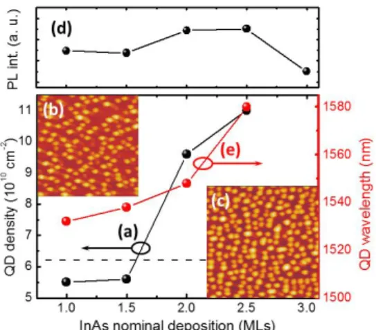
Figure 1(a) reveals the QD density measured on a single uncapped QD layer as a function of the nominal thickness of InAs in MLs. By increasing the thickness of InAs from 1 to 2.5 ML, the QD density was increased from 5x1010 cm-2 (Fig. 1(b)) up to value of 11x1010 cm-2 (Fig. 1(c)).
Such high-density QDs (HD-QD) are placed in close proximity, with typical layer-to-layer separation of 30-40 nm. The integrated photoluminescence variation as a function of the InAs thickness is presented at Fig. 1(d). No significant intensity variation is observed with InAs thickness up to 2.5 MLs. Further increase of InAs nominal thickness above 2.5 ML leads to QDs coalescence and formation of large and plastically relaxed QDs, leading to the decrease of PL efficiency. This fact evidencing formation of non-radiative recombination centers, which can prohibit VECSEL operation. Furthermore, Fig.1(e) shows the evolution of the QD wavelength emission at room temperature, derived from PL spectra. Simultaneously with the QD density increase, the QD height increases as evidenced by the continuous redshift of the QD from 1530 nm to 1580 nm. In the case of InAs/InP QDs, independent control between QD density and wavelength emission can be achieved by applying a double-cap (DC) growth sequence. 13
FIG. 1. QD density (a) and emission wavelength (e) variation as function of InAs thickness (in MLs). Insets (b) and (c) are AFM scans (0.5x0.5 µm²) of the uncovered QDs for InAs thickness of 1 and 2.5 MLs respectively. Dotted line represents the
target wavelength at 1515 nm. (d) Integrated photoluminescence intensity of a single QD layer as function of InAs MLs.
Figure 2(a) reveals the PL spectrum of a single layer of high density (HD)-QD as-grown sample, while Fig.2(b) presents PL of the sample grown accordingly to the DC procedure. To decrease HD-QD emission wavelength, the DC growth process was applied at the same QD growth temperature. At first 2.8 nm thick cap layer of Q1.18 was deposited on the QDs and followed by a 20 seconds growth interruption under mixture of AsH3+PH3 overpressure flux. 14 Thus, HD-QDs
with central wavelength at 1517 nm with full width at half maxima (FWHM) of 115 nm have been fabricated. Stacking of QD layers, separated by spacer layers (SLs), was performed in order to further increase the gain volume. Since QD formation is governed by strain effects, the thickness of the SL between two QD layers is known to play an important role on the upper QD layer. Thicker SL has been shown to decrease the upper QD layer density because of size filtering effects. Thinner SL enables keeping QD density per layer constant due to strain mediated vertical alignment of QDs, however strain accumulation still limits the number of defect-free stacked layers.15,16 Consequently, when considering QD as active layer in photonic devices, optimal
thickness of SL typically lies around 25-40 nm in order to avoid any defects, which also enables to stack up to 10 layers when necessary. When dealing with VECSELs, such thick SL limits the number of QD layers per electric field antinode to approximately three layers. In order to realize QD stacking with a reduced SL thickness, we have used a strain compensation technique,17 thus
after the growth of the first DC HD-QD, slightly tensile stressed 15-nm thick Q1.18 SL has been grown in order to mitigate strain effect for the next QD layer. This cycle has been carried out five times. Figure 2(c) shows the PL spectrum of the QD layers stack sample. The wavelength emission and linewidth of the QD stack is identical to that of single DC HD-QD sample. Furthermore, PL intensity of the stack has been increased threefold evidencing the good optical quality of these QD layers.
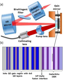
Following these QD growth optimizations, we have developed a VECSEL gain structure illustrated in Fig.3(b). The structure is composed of the InP-based QD active region and a GaAs-based distributed Bragg reflector, which was grown by metalorganic vapor-phase epitaxy (MOVPE). The gain section consists of 20 QDs layers arranged into four groups of five DC HD-QD with 15 nm thick SLs. Each group was placed at the antinode of the micro-cavity electric field formed between DBR and a top-surface of the gain region. Subsequently, the InP-based QD gain structure was wafer-fused to a DBR composed of 29.5 AlAs/GaAs pairs, following the fusion process described by A. Sirbu et al.18
FIG.2. PL spectra of a single layer of as grown HD-QD (a), and DC HD-QD (b) measured at 300K and with the same input power density (500 W/cm²). PL spectrum of 5 DC HD-QD layers with 15 nm spacer layers (c) before fusion of DBR. Eye guide
dashed line placed at 1510 nm.
After the wafer fusion and selective etching of InP substrate the resulting wafer was cleaved into rectangular chips (2.7x2.7 mm2), which were subsequently capillary bonded to an uncoated
intra cavity diamond heat spreader, with dimensions of 3x3x0.35 mm3. The chip-diamond
assembly was mounted onto a thermoelectrically cooled copper plate, which was kept at 15 °C throughout the measurements. The structure was tested in a V-shape resonator, which is shown in Fig. 3(a) and is composed of a highly reflective mirror (R>99.8%) with curvature radius of 200 mm and a flat output coupler with reflectivity of 99%. The distance between gain mirror and curved mirror was 150 mm, while the distance between curved mirror and output coupler was 276 mm; such resonator geometry provided a calculated mode diameter of 190 µm on the gain mirror. The VECSEL was pumped by a 980 nm fiber coupled diode laser, which collimated output was focused down to a pump spot with a diameter of ~220 µm. A birefringent filter with a thickness of 0.5 mm was used for tuning measurements and was placed at a Brewster angle inside the cavity.
FIG.3. Schematics of V-shaped cavity with inserted birefringent filter for tuning measurements (a) and gain mirror structure (b).
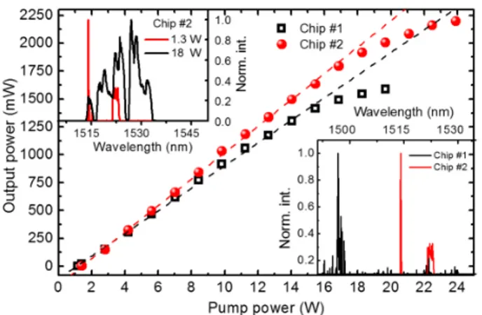
Figure 4 shows the output power and threshold spectra (lower inset) of two exemplary VECSELs chips with different detuning (offset between micro-cavity resonance wavelength and PL peak). Upper inset shows spectra of one of the chips at different incident pump powers. The maximum output power was measured to be 2.2 W at 24 W of incident pump power, resulting in 11.7% of slope efficiency (nominal incident power was used for the fit).
Unlike QWs, PL peak of QDs undergoes thermal red shift at a much slower rate, by this resulting in a considerably smaller detuning factor. The measured threshold spectra, recorded at 1.4 W of incident pump power, allow approximate estimation of micro cavity resonances of the chips. Thus, the optimal detuning factor was experimentally determined by testing chips across the wafer, since variation of micro cavity resonance corresponds to active region thickness fluctuation across the wafer. Although the slope curves of the two demonstrated chips are virtually identical at low pump powers (due to broad QD gain), closer to thermal roll-over the chip #1 with a larger detuning becomes less efficient, yielding lower output powers. The optimal detuning value gains significance in the context of the resonant micro cavity, where the round trip gain directly depends on overlap factor between the electric field antinodes and the QDs packages within micro cavity.19
FIG.4. Output power and threshold spectra of the free-running VECSELs, measured at 15°C. Chips were taken from across the wafer, exhibiting different micro cavity resonances.
The wavelength tuning ability is shown in Fig.5; the tuning was achieved with the intra cavity birefringent filter. Operation in a wavelength window of about 60 nm was obtained from the single chip. The tuning curve was recorded under an incident pump power of 6 W. Inset of Fig. 5 shows exemplary beam profile measured at 22 W of incident pump power, revealing a slightly elliptical beam profile due to V-shape resonator geometry.
FIG. 5. Wavelength tuning recorded as a function of birefringent filter rotation. The figure is composed from nine different spectra. Tuning obtained with the chip #2 under the incident power of 6 W.
In conclusion, implementation of DC growth sequence coupled with optimization of SL thickness by means of strain compensation allowed to demonstrate an InP-based QD gain mirror comprising dense QD layers. Such gain structure enabled demonstration of the first QD-based VECSEL emitting at 1.5 µm with output power of 2.2 W. The emission wavelength could be tuned over 60 nm using an intra cavity birefringent filter. In terms of output power the results obtained with this type of gain mirror are on par with earlier demonstrations for quantum well-based
VECSELs at the same wavelength range,20 yet opening the way for superior performance in terms
of broadband tuning, temperature stability and lower threshold.
Second-harmonic generation of the VECSEL with emission at 1.5 µm constitutes a viable alternative to 750 nm direct emitting VECSEL,21, 22 by offering much longer lifetime and wider
wavelength tunability. In turn, lasers at 750 nm range are needed for isotope separation,23
spectroscopy, 24 and in medicine due to the large penetration depth into tissues at the wavelengths
around 750 nm.25
This work has been partly supported by Agence Nationale de la Recherche (ANR) and Suisse National Science Foundation (ANR-SNSF IDYLIC project, grant ANR-15-CE24-0034-01).
1M. Kuznetsov, F. Hakimi, R. Sprague and A. Mooradian, IEEE Photon. Technol. Lett. 9, 1063, (1997).
2M. Stephane Calvez, J. E. Hastie, M. Guina, O. G. Okhotnikov, and M. D. Dawson, Laser & Photon. Rev. 3, 407, (2009). 3M. Guina, A. Rantamäki and A. Härkönen, J. Phys. D: Appl. Phys. 50, 1, (2017).
4B. W. Tilma, M. Mangold, C. A. Zaugg, S. M. Link, D. Waldburger, A. Klenner, A. S. Mayer, E. Gini, M. Golling and U. Keller, Light Sci.
Appl. 4, 1, (2015).
5M. Butkus, J. Rautiainen, O. G. Okhotnikov, S. S. Mikhrin,I. L. Krestnikov and E. U. Rafailov, in Proc. 22nd IEEE Int. Semiconductor Laser
Conf. (ISLC), Kyoto, Japan, Sep. 2010, pp. 71–72.
6
D. Al Nakdali, M. Khaled Shakfa, M. Gaafar, M. Butkus, K. A. Fedorova, M. Zulonas, M. Wichmann, F. Zhang, B. Heinen, A. Rahimi-Iman, W. Stolz, E. U. Rafailov and M. Koch, IEEE Photon. Technol. Lett. 26, 1561, (2014).
7T. D. Germann, A. Strittmatter, J. Pohl, U. W. Pohl, D. Bimberg, J. Rautiainen, M. Guina and O. G. Okhotnikov, Appl. Phys. Lett. 93, 051104,
(2008).
8M. Butkus, J. Rautiainen, O. G. Okhotnikov, C. J. Hamilton, G. P. A. Malcolm, S. S. Mikhrin, Igor L. Krestnikov, D. A. Livshits and
E. Rafailov, IEEE J. Sel. Top. Quantum Electron., 17, 1763, (2011).
9T. Schwarzbäck, R. Bek, F. Hargart, C. A. Kessler, H. Kahle, E. Koroknay, M. Jetter and P. Michler, Appl. Phys. Lett. 102, 092101, (2013). 10P. J. Schlosser, J. E. Hastie, S. Calvez, A. B. Krysa and M. D. Dawson, Opt. Exp. 17, 21782, (2009).
11P. Caroff, C. Paranthoen, C. Platz, O. Dehaese, H. Folliot, N. Bertru, C. Labbé, R. Piron, E. Homeyer, A. Le Corre and S. Loualiche, Appl.
Phys. Lett. 87, 243107, (2005).
12A. Becker, V. Sichkovskyi, M. Bjelica, A. Rippien, F. Schnabel, M. Kaiser, O. Eyal, B. Witzigmann, G. Eisenstein and J. P. Reithmaier,Appl.
Phys. Lett. 110, 181103, (2017).
13C. Paranthoen, N. Bertru, O. Dehaese, A. Le Corre, S. Loualiche and B. Lambert, Appl. Phys. Lett. 78, 1751, (2001). 14P. Caroff, N. Bertru, C. Platz, O. Dehaese, A. Le Corre, and S. Loualiche, J. Crys. Growth 273, 357, (2005). 15Q. Xie, A. Madhukar, P. Chen and N. P. Kobayashi, Phys. Rev. Lett. 75, 2542, (1995).
16L. Li, G. Patriarche, N. Chauvin, P. Ridha, M. Rossetti, J. Andrzejewski, G. Sek, J. Misiewicz and A. Fiore, IEEE J. Sel. Top. Quantum
Electron. 14, 1204, (2008).
17K. Akahane, N. Yamamoto and T. Kawanishi, IEEE Photonic. Tech. Lett. 22, 103, (2010).
18A. Sirbu, V. Iakovelv, A. Mereuta, A. Caliman, G. Suruceanu and E. Kapon, Semicond. Sci. Technol. 26, 014016, (2011). 19F. Zhang, C. Möller, M. Koch, W. S. Koch, A. Rahimi-Iman and W. Stolz, Appl. Phys. B 123, 291, (2017).
20A. Rantamäki, J. Rautiainen, J. Lyytikäinen, A. Sirbu, A. Mereuta, E. Kapon and O. G. Okhotnikov, Opt. Express 20, 9046, (2012). 21H. Kahle, K. Nechay, J.-P. Penttinen, A. Tukiainen, S. Ranta, and M. Guina, Opt. Lett. 43, 1578 (2018).
22K. Nechay, H. Kahle, J.-P. Penttinen, P. Rajala, A. Tukiainen, S. Ranta, and M. Guina, IEEE Photonic. Tech. Lett. 31, 1245, (2019). 23T. Mazur, B. Klappauf, and M. Raizen, Nat. Phys. 10, 601, (2014).
24L.Gianfrani, R. W. Fox, and L. Hollberg, J. Opt. Soc. Am. B 16, 2247, (1999). 25S. L. Jacques, Phys. Med. Biol. 58, 5007, (2013).