HAL Id: hal-00920110
https://hal.archives-ouvertes.fr/hal-00920110
Submitted on 17 Dec 2013HAL is a multi-disciplinary open access archive for the deposit and dissemination of sci-entific research documents, whether they are pub-lished or not. The documents may come from teaching and research institutions in France or abroad, or from public or private research centers.
L’archive ouverte pluridisciplinaire HAL, est destinée au dépôt et à la diffusion de documents scientifiques de niveau recherche, publiés ou non, émanant des établissements d’enseignement et de recherche français ou étrangers, des laboratoires publics ou privés.
Importance of Spin-Orbit Coupling in Hybrid
Organic/Inorganic Perovskites for Photovoltaic
Applications
Jacky Even, Laurent Pedesseau, Jean-Marc Jancu, Claudine Katan
To cite this version:
Jacky Even, Laurent Pedesseau, Jean-Marc Jancu, Claudine Katan. Importance of Spin-Orbit Cou-pling in Hybrid Organic/Inorganic Perovskites for Photovoltaic Applications. Journal of Physical Chemistry Letters, American Chemical Society, 2013, 4 (7), pp.2999-3005. �10.1021/jz401532q�. �hal-00920110�
Importance of spin-orbit coupling in hybrid
organic/inorganic perovskites for photovoltaic
applications
Jacky Even,†Laurent.Pedesseau,†Jean-marcJancu,† and ClaudineKatan*‡
†Université Européenne de Bretagne, INSA, FOTON, UMR 6082, 35708 Rennes, France ‡CNRS, Institut des Sciences Chimiques de Rennes, UMR 6226, 35042 Rennes, France
Corresponding Author
Claudine Katan
Three-dimensional organic/inorganic perovskiteshave recently been suggested as a novel class of materials for dye-sensitized solar cells (DSSC) with improved photo-conversion efficiency.These compounds are modeledin this work within the density functional theory (DFT). The band-gaps aredominated by a giant spin-orbit coupling (SOC) in the conduction-band, which has been largely overlooked so far. Direct and isotropic optical transitions at room temperature are
associated to a spin-orbit split-off band related to a triply degenerated conduction-band of the cubic lattice without SOC. It is shown that, due to the strong SOC, the electronic states involved in the optical absorption are only slightly perturbed by local distortions of the lattice. In addition, band offset calculations confirm that CH3NH3PbX3/TiO2 (X=Br, I) is a reference material for
driving electrons toward the electrode in dye-sensitized solar cells. Two dimensional hybrid perovskites are also suggested to reach further flexibility for light conversion efficiency. This study is a major step towards the understanding of the optoelectronic properties of these novel class of DSSC at the level of knowledge already achieved in the field of conventional semiconductors.
Hybrid materials, optoelectronics, titanateoxyde, density functional theory
Photovoltaic (PV) solar electricity is one of the key technologies of the 21st century to reduce the world’s reliance on fossil fuels for energy generation. Reduced costs and higher conversion efficiencies are of crucial importance to make PV-based technologies economically more competitive. The quest for quality and performances of future solar cells has attracted a vast research effort over the last decade in the field of semiconductor heterostructures, nanostructured materials, and thin films. Various approaches ranging from high-cost/high-performance III-V technologies, multiple junctions and concentrator systems, to low-cost thin-films technologies1-4
realistic modeling of underlying material’s properties including chemical composition, mechanical, electrical and optical features. This can be gained with state-of-the-art ab-initio approaches. In addition, such knowledge is desirable to reach PV cells composed of earth-abundant elements based materials.
Three-dimensional organic/inorganic perovskites, based on relatively small organic cations, have recently been suggested as a novel class of materials for dye-sensitized solar cells (DSSC) with improved photo-conversion efficiency.5-17Indeed, with a nanoporous TiO2 electrode, ultra-high
light power conversion efficiencies have been demonstrated. Compared to alternative strategies based on inorganic semiconductor quantum dots (QDs) or extremely thin absorbers coated upon the internal surface of a mesoporous TiO2 electrode, hybrid perovskites offer several benefits. In
particular, the ease of synthesis, tailoring of the optical absorption by chemical substitution, electronic transport, and high stability in dry air, are among the most featured properties of these systems. Interestingly, whereas conduction-band and valence-band alignments between
absorbers and TiO2 are of crucial importance in understanding charge transfer and charge
transport,7,8,16,18 their modeling is still scanty.
Conversely, two dimensional hybrid organic/inorganic materials have attracted increasing interest over the past decade due to their potential optoelectronic applications.19 Once more, the versatility of the organic part affords the possibility of fine tuning material’s properties. For example, it has been shown that the optical spectra of lead halide organic/inorganic perovksites can be easily tailored by varying the organic cation, which improves the optical efficiencies and tuning of the emission wavelength.19 Among them, self-assembled layered structures have recently shown enhanced non-linear optical properties in microcavities.20 Interestingly, in these
tetrahedrally-bonded semiconductors.21 Consistently with important relativistic effects expected for lead, such calculations have also evidenced the major role of spin-orbit coupling (SOC) that significantly reduces the band-gap by inducing a large splitting of the first degenerated
conduction levels.21
Surprisingly, for the hybrid 3D materials recently proposed as efficient DSSC,5,7,8,14-16 the effect of SOC has been largely overlooked, especially from the theoretical point of view. Optical absorption22and reflectivity23 measurements brought clear experimental evidence of sizeable SOC splittings in such materials more than a decade ago. Even so effects of SOC have been stressed in a recent computational work,15 to the best of our knowledge they have not yet been accounted for in calculated band structures reported in the literature.
This paper aims to investigate the role of SOC on the electronic band structure of two 3D hybrids recently investigated for PV-devices, namely MAPbX3 compounds where X=Br,I and MA stands
for methylammonium (CH3NH3). Moreover, as the design of efficient DSSC requires a good
understanding of VB alignments, we suggest a protocol to derive the band alignment between the MAPbX3 absorbers and TiO2. It involves calculations on a slab of a related 2D hybrid, namely
2(C4H9NH3+)(PbI42-).24 Such analogs also allow further comparison and offer complementary
routes for band gap engineering. Actually, by mixing the composition of halogen atoms in
MAPb(I1-xBrx)3 structures, it has recently been shown that the band gap can be controllably tuned
to cover the entire visible spectrum.14
These mixed compounds exhibit an averaged disordered cubic phase (space group Pm3m) at room temperature.25The structural disorder is both associated to the rotation of ammonium cations and tilt of lead halide octaedra. At low temperature, MAPbBr3 and MAPbI3 present an
ordered orthorhombic structure of space-group Pnma, with a cell doubling when compared to the room temperature phase(Figure 1).15,26
Figure 1.Overview of the crystal structures of MAPbI3(left) and MAPbBr3(right) at low
temperature. The structures are both orthorhombic (space group Pnma),15,26with a cell doubling when compared to the room temperature cubic phase.
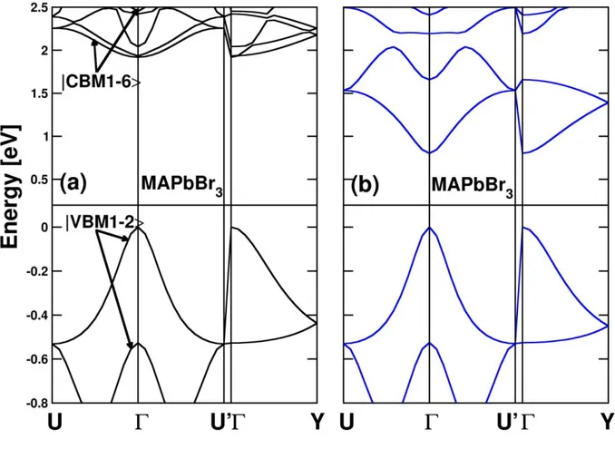
These ordered crystalline structures are used to perform the present theoretical study. Figure 2 shows the band structures of MAPbBr3 and MAPbI3 with and without the SOC interaction.
Figure 2.Electronic band structures of MAPbI3 (top) and MAPbBr3 (bottom), without (a) and
with (b) the spin-orbit coupling interaction. The origin of the energy scale is taken at the top of the valence band (VBM).
Let us first analyze the results obtained without SOC. Consistently with earlier results on the room temperature cubic phase,27the ground state transitions are of direct type but at the -point instead of the R point.15 Our study shows that they mainly involve eight active Bloch levels: two levels for the valence-band maximum (VBM1-2) and six levels for the conduction-band
minimum (CBM1-6). This apparent complex sequence at -pointis associated to the low temperature symmetry breaking which leadsboth to unit cell doubling and strain.26In fact, a symmetry analysis indicates that the CBM1-6 states are related to the conduction-band minimum
(CBM)at the R point in the room temperature Pm3m cubic phase which corresponds to a triply-degenerate level associated to the vectorial representation of the simple group.25The same electronic band structure is obtained around the band gap for the related CsPbI3compound where
the organic part of MAPbI3is replaced by a Cs atom in the low temperature Pnma phase (figure
S1). We canfurther develop the analysis of the electronic states using the complete phase sequence ofMAPbI3 and CsPbI3structures (vide infra). Similar energy dispersions occur at low
temperature along the -U (1/2,0,1/2), -Y and -U’ (1/2,0,-1/2) directions in figure 2, which is inherent to the small distortion of the perovskite lattice. The direct band-gap calculated at -pointis in agreement with the strong absorbance observed at room temperature.7,22 The six CBM1-6states correspond to anti-bonding hybridizations of 6p-orbitals of lead and belong to the irreducible representations of the D2h point group (factor group for the Pnmaspace group at
point). VBM1-2consist in anti-bonding hybridizations of the 6s-orbitals of lead and 5p-orbitals of iodine and are associated to non-polar irreducible representations of the point group. Optical activity is related to the dipolar matrix elements between the first valence and conduction-band states as defined by: , 13 13
CBM i VBM CBM VBM x i
M where xi represents the crystal
axis.21These matrix elements take similar values for the CBM states in the MAPbX3 family. A
strong and almost isotropic optical activity is expected from symmetry and enhanced at room temperature by the disorder of the cubic phase. Similar results are obtained for MAPbI3, although
the strain-induced conduction-band splitting is larger. We point out that a strain effect was also reported in related MASnX3 compounds.32
Figure 2 reveals large changes of the electronic band structure when accounting for SOC. Indeed, the fundamental transitions of MAPbI and MAPbBr lower to 0.5eV and 0.8eV respectively.
While the VB are nearly unaffected, the sixfirst CB undergo a dramatic splitting. The band gap remains direct and located at the center of the Brillouin zone. These findings are consistent with the value reported for a related 2D organic–inorganic hybrid, 2(pF-C6H5C2H4–NH3)PbI4, for
which the correction is of about 1eV, leading to a band-gap reduction by a factor of two.21This 2D perovskite crystalizes similarly to the 2(AA)PbX4 family (AA= CnH2n+1NH3)24,29,30 for which
we have employed the same level of theory. For n=4-12 and X=I, the spin-orbit coupling induces a large band-gap correction of about 0.8eV, again mainly localized on the CB levels. Moreover, when applied to related inorganic structures such as CsPbX3, comparable corrections are
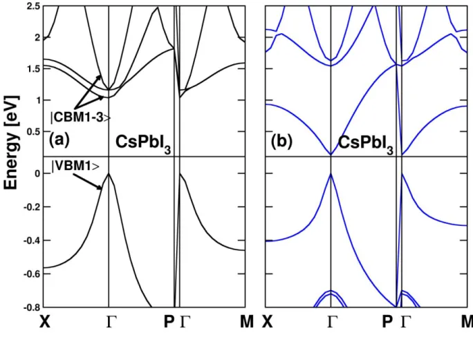
obtained, as illustrated figure 3(top) for the inorganic cubic phase of CsPbI3(a similar result
Figure 3..Electronic band structures of CsPbI3 in the cubic phase (top) and tetragonal phase (bottom), without (a) and with (b) the spin-orbit coupling interaction. The origin of the energy scale is taken at the top of the valence band (VBM).
One can notice that the calculated band-gap at the GGA-PBE level is equal to 1.3eV in good agreement with previous simulations.36. The calculated band-gaps at the LDA level are equal to 1.2eV for CsPbI3and 1.3eV for CsPbBr3, and the spin-orbit coupling induces a large band-gap
correction of about 1.1eV in both cases (figure 3(top)). All these results demonstrate that the effect of SOC on band gaps is huge and cannot be reasonably disregarded. Even if comparison with available experimental data is not straightforward, our results are in qualitative good agreement with evidence of SOC effects in the optical absorption22 and reflectivity23 spectra
reported for MAPbX3. Furthermore, the optical transition occurs at the R point in the room
temperature Pm3m cubic phase. For the Pm3msymmorphic space group, it is possible to directly analyzethe irreducible representations at R point using the Oh point group.31 The
triply-degenerate (CBM1-3) (figure 3-a (top)) statesare associated to the vectorial representation of the simple group commonly described21,32 by the X , Y , Z symbols. In the corresponding double groupincludingspinors, it is splitted by SOC into twofold degeneratestates and fourfold degenerate states (figure 3-b (top)). This situation is usually encountered in the valence band of cubic conventional semiconductors.21,31 The conduction band minimum of CsPbX3 and MAPbX3
at room temperature are associated to the twofold degenerate spin-orbit split-off (SO) states
X iY Z 3 1 3 1 2 / 1 , 2 / 1 and
XiY
Z 3 1 3 1 2 / 1 , 2 / 1 (figure3-b (top)).The SO states lead to a strong21 and isotropic32optical transition with the even S -like VBM states.To understand the influence of the cubic-tetragonal (Pm3m-I4mcm) transition of MAPbI333 on its optoelectronic properties, we have also performed DFT calculations on CsPbI3in
the tetragonal phase of MAPbI3including the SOC. Without SOC, the triply degenerate CBM
states and the VBM state are folded back from the R point at the pointcases (figure 3a, bottom). In addition and according to the D4h point group, the strain along the z axis inducesa small splitting of the CBM and the band gap reduces to 1.0eV. The CBM vectorialrepresentation splits into a non-degenerate Z state at lower energy and twofold degenerate X , Y states. The SOC effect is however much larger than the effect of strain, and leads to a very small band gap (figure 3b(bottom)). The state ordering including SOC at the point of the I4mcm phase remains similar to the one of the Pm3m cubic phase, the CBM states being again related to the twofold degenerate SO states 1/2,1/2 and 1/2,1/2 .
Based on the band structure of CsPbI3, we can also investigate the cubic-orthorhombic
(Pm3m-Pnma) transition. This transition is associated to a cell doubling and folding back from the R point to the point. The triply degenerate CBM are doubled and splitted by the strain along the three directions. The six CBM states correspond to one dimensional representations of the simple D2h point group which yield two-fold degenerate representations of the corresponding double
group. The strain effect is no more negligible when compared to the SOC effect, but the CBM state of lowest energy has an electronic density similar to the one of cubic SO state.
Now, one can wonder why the fundamental transitions calculated without SOC for the low temperaturePnma structures, 1.5 eV and 1.9 eV respectively for MAPbI3 and MAPbBr3 (figure
2) compare nicely with the values obtained experimentally, i.e. 1.5eV and 2.3eV respectively for MAPbI3 and MAPbBr3.5,14,22,23 This agreement is fortuitous and stems from large error
cancellations. Indeed, the band gap is known to be underestimated in the DFT ground-state computations. This can be corrected by including many-body effects by means of GW self-energy correction for the band gap34 or using the Bethe Salpeter equation resolution for the exciton.35Unfortunately, such calculations are beyond available computational resources for large systems. In order to gauge the importance of the GW corrections, we have considered the cubic phase of CsPbI3. A one-shot GW self-energy correction on the LDA level amounts to a
0.6 eV increase of the band gap. This value, although not self-consistent, shows that GW
corrections are large and in the opposite direction to SOC effects. Unfortunately, a full treatment including both SOC and many-body effects is far beyond available computational resources. Efficient electrical power generation relies on the quality of the absorber and the band-gap energy. These conditions appear to be fulfilled and understood from the theoretical point of view.
electrodes. A correct band alignment between the sensitizer and the electrode materials is thus a key parameter to predict performances of PV devices. In the case of DSSC, with a TiO2
electrode, hybrid MAPbX3perovskites appear to greatly improve the electron transport.8 To
evaluate the valence-band alignment between the anatase structure of TiO28 and hybrid
perovskites, a slab calculation37 was performed for the 2(AA)PbI4 with n=4. This allows
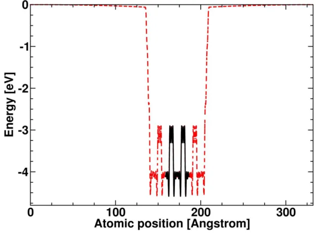
estimating the offsets between the vacuum level and its bulk potential (figure 4).
Figure 4.Potential profile in an alkyl ammonium (AA) 2D hybrid perovskite crystal (dark line)
and in a slab (red dotted line) with the same crystallographic structure24 surrounded by
vacuum.An upward energy shift equal to 0.93eV has been applied to the crystal profile in order to match the slab profile. When the same shift is applied to the computed VBM, an absolute
It leads to an absolute valence-band energy of -5.6 eV. Moreover, one can use the position of the 5d levels of lead as a common electronic marker both for 3D and 2D hybrid perovskites. The relative position of the 5dorbitals with respect to their VBM amount respectively to 16.4 and -16.2 eV. This leads to an absolute valence-band energy of -5.4 eVfor both MAPbX3 crystals that
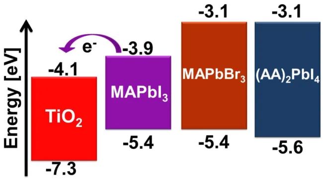
nicely agrees with the absolute valence-band energy levels deduced from the experimental work functions: -5.44 and -5.38 eV for X=I and X=Br, respectively.5 The complete band alignment diagram is given figure 5, based on the absolute valence-band energy (-7.3eV) commonly used for TiO2.8
Figure 5.Energy level diagram derived from the position of Pb-5d orbitals, computed VBM
(figure 4) and experimental band gaps of MAPbI3 (1.5eV), MAPbBr3 (2.3eV)5,14 and an alkyl
ammonium (AA) 2D hybrid perovskite (2,5 eV).24 Commonly accepted values for TiO2 electron
It clearly demonstrates that the conduction-band offsets are favorable for the electron injection from absorber to electrode. In addition, this diagram suggests that combining 2D and 3D hybrid perovskites may provide an alternative way for the design of colorful solar cells that cover the entire visible spectrum.
In summary, based on DFT calculations, the electronic properties of 3D lead halide organic/inorganic perovskites used as absorbers in DSSC5,7,8 have been thoroughly investigated. Their band-gap is dominated by a giant SOC effect acting mainly on the conduction band, as was already demonstrated for related 2D hybrids.21 At room temperature, their remarkable optical properties can be related to direct and isotropic optical transitions between a triply degenerated conduction-band and a single valence-band in a simple group representation. Valence band offsets5 confirm that the gathering of MAPbX3 hybrids and TiO2 is a relevant choice for driving
the electrons toward the electrode. Our calculations on alkyl ammonium based 2D hybrids also suggest a complementary route to the chemical tuning14 recently proposed for the design of colorful solar cells with enhanced light conversion efficiency.
The present theoretical study was performed using the DFT implementation available in the ABINIT package,38 with the LDA or the GGA-PBE gradient correction for exchange-correlation39 and relativistic, norm-conserving, separable, dual-space Gaussian-type pseudopotentials of Goedecker, Teter, and Hutter for all atoms40or Fritz-Haber-Institute’s pseudpotentials.41The SIESTA code was used for the simulation of slabs at the DFT-GGA level.42 We have verified that the band structures near the band-gap do not depend on the inclusion of 5d-orbitals for Pb. The electronic wave-functions are expanded onto a plane-wave basis set with an energy cut-off of 950 eV. 4x4x4 and 4x4x1 Monkhorst-Pack grids are used for
reciprocal space integration in 3D and 2D structures respectively. Calculations were performed with and without SOC.
Corresponding Author
*Email: claudine.katan@univ-rennes1.fr Tel: +33 (0)2 23 23 56 82
Notes
The authors declare no competing financial interests.
This work was performed using HPC resources from GENCI-CINES/IDRIS grant
2013-c2012096724. The work is supported by AgenceNationale pour la Recherche (PEROCAI project ANR-10-04).
(1) Feltrin, A.; Freundlich, A., Material considerations for terawatt level deployment of photovoltaics. Renewable Energy 2008,33 (2), 180-185.
(2) Oregan, B.; Grätzel, M., A Low-cost, high-efficiency solar-cellbasedon dye-sensitizedcolloidalTiO2films. Nature1991,353 (6346), 737-740.
(3) Grätzel, M., Solar energy conversion by dye-sensitized photovoltaic cells. Inorg. Chem. 2005,44 (20), 6841-6851.
(4) Almosni, S.; Robert, C.; Thanh, T. N.; Cornet, C.; Letoublon, A.; Quinci, T.; Levallois, C.; Perrin, M.; Kuyyalil, J.; Pedesseau, L.; Balocchi, A.; Barate, P.; Even, J.; Jancu, J. M.; Bertru, N.; Marie, X.; Durand, O.; Le Corre, A., Evaluation of InGaPN and GaAsPN
materials lattice-matched to Si for multi-junction solar cells. J. Appl. Phys.2013,113 (12), 123509-123509-6.
(5) Kojima, A.; Teshima, K.; Shirai, Y.; Miyasaka, T., Organometal Halide Perovskites as Visible-Light Sensitizers for Photovoltaic Cells. J. Am. Chem. Soc.2009,131 (17), 6050-6051.
(6) Im, J. H.; Lee, C. R.; Lee, J. W.; Park, S. W.; Park, N. G., 6.5% efficient perovskite quantum-dot-sensitized solar cell. Nanoscale2011,3 (10), 4088-4093.
(7) Lee, M. M.; Teuscher, J.; Miyasaka, T.; Murakami, T. N.; Snaith, H. J., Efficient Hybrid Solar Cells Based on Meso-SuperstructuredOrganometal Halide Perovskites. Science
2012,338 (6107), 643-647.
(8) Etgar, L.; Gao, P.; Xue, Z. S.; Peng, Q.; Chandiran, A. K.; Liu, B.; Nazeeruddin, M. K.; Gratzel, M., Mesoscopic CH3NH3PbI3/TiO2Heterojunction Solar Cells. J. Am. Chem.
Soc.2012,134 (42), 17396-17399.
(9) Kim, H. S.; Lee, C. R.; Im, J. H.; Lee, K. B.; Moehl, T.; Marchioro, A.; Moon, S. J.; Humphry-Baker, R.; Yum, J. H.; Moser, J. E.; Grätzel, M.; Park, N. G., Lead Iodide Perovskite Sensitized All-Solid-State Submicron Thin Film Mesoscopic Solar Cell with Efficiency Exceeding 9%. Sci. Rep.2012,2, 591-591-7.
(10) Heo, J. H.; Im, S. H.; Noh, J. H.; Mandal, T. N.; Lim, C. S.; Chang, J. A.; Lee, Y. H.; Kim, H. J.; Sarkar, A.; Nazeeruddin, M. K.; Grätzel, M.; Seok, S. I., Efficient
inorganic-organic hybrid heterojunction solar cells containing perovskite compound and polymeric hole conductors. Nat. Photonics 2013, 7 (6), 487-492.
(11) Ball, J. M.; Lee, M. M.; Hey, A.; Snaith, H. J., Low-temperature processed meso-superstructured to thin-film perovskite solar cells. Energy & Environmental Science
2013,6 (6), 1739-1743.
(12) Baikie, T.; Fang, Y. N.; Kadro, J. M.; Schreyer, M.; Wei, F. X.; Mhaisalkar, S. G.; Graetzel, M.; White, T. J., Synthesis and crystal chemistry of the hybrid perovskite (CH3NH3) PbI3 for solid-state sensitised solar cell applications. J. Mater. Chem. A 2013,1
(18), 5628-5641.
(13) Qiu, J. H.; Qiu, Y. C.; Yan, K. Y.; Zhong, M.; Mu, C.; Yan, H.; Yang, S. H., All-solid-state hybrid solar cells based on a new organometal halide perovskite sensitizer and one-dimensional TiO2 nanowire arrays. Nanoscale2013,5 (8), 3245-3248.
(14) Noh, J. H.; Im, S. H.; Heo, J. H.; Mandal, T. N.; Seok, S. I., Chemical Management for Colorful, Efficient, and Stable Inorganic-Organic Hybrid Nanostructured Solar Cells. Nano Lett.2013,13 (4), 1764-1769.
(15) Mosconi, E.;Amat, A. ; K. Nazeeruddin, Md. ; Grätzel, M. ; De Angelis, F., First Principles Modeling of Mixed Halide OrganometalPerovskites for Photovoltaic
Applications. J. Phys Chem. C 2013 (DOI: 10.1021/jp4048659)
(16) Park, N.G.,OrganometalPerovskite Light Absorbers Toward a 20%
EfficiencyLow-Cost Solid-State Mesoscopic Solar CellJ. Phys Chem. Lett. 2013, 4, 2423-2429.
(17) Burschka, J.; Pellet, N.; Moon, S.J.; Humphry-Baker, R.; Gao, P.; Nazeeruddin, M.K.; Grätzel, M.; Sequential deposition as a route to high-performance perovskite-sensitized solar cells Nature2013499, 316–319.
(18) Itzhaik, Y.; Hodes, G.; Cohen, H., Band Alignment and Internal Field Mapping in Solar Cells. J. Phys. Chem.Lett.2011, 2 (22), 2872-2876.
(19) Mitzi, D. B.; Wang, S.; Feild, C. A.; Chess, C. A.; Guloy, A. M., Conducting layered organic-inorganic halides containing (110)-oriented perovskite sheets. Science
1995,267 (5203), 1473-1476.
(20) Wei, Y.; Lauret, J. S.; Galmiche, L.; Audebert, P.; Deleporte, E., Strong exciton-photon coupling in microcavities containing new fluorophenethylamine based perovskite compounds. Opt. Express2012,20 (9), 10399-10405.
(21) Even, J.; Pedesseau, L.; Dupertuis, M. A.; Jancu, J. M.; Katan, C., Electronic model for self-assembled hybrid organic/perovskite semiconductors: Reverse band edge electronic states ordering and spin-orbit coupling. Phys. Rev. B 2012,86 (20), 205301-205301-4.
(22) Tanaka, K.; Takahashi, T.; Ban, T.; Kondo, T.; Uchida, K.; Miura, N., Comparative study on the excitons in lead-halide-based perovskite-type crystals CH3NH3PbBr3CH3NH3PbI3. Solid State Comm.2003,127 (9-10), 619-623.
(23) Hirasawa, M.; Ishihara, T.; Goto, T., Excitonfeaturesin 0-dimensional,
2-dimensional, and 3-dimensionalnetworksof PbI6 4-octahedra. J. Phys. Soc. Jap.1994,63
(10), 3870-3879.
(24) Billing, D. G.; Lemmerer, A., Synthesis, characterization and phase transitions in the inorganic-organic layered perovskite-type hybrids (CnH2n+1NH3)(2)PbI4 , n=4, 5 and 6.
(25) Poglitsch, A.; Weber, D., Dynamicdisorderin
methylammoniumtrihalogenoplumbates(II) observed bymillimeter-wave spectroscopy. J.
Chem. Phys.1987,87 (11), 6373-6378.
(26) Swainson, I. P.; Hammond, R. P.; Soulliere, C.; Knop, O.; Massa, W., Phase transitions in the perovskitemethylammonium lead bromide, CH3ND3PbBr3. J. Solid
State Chem.2003,176 (1), 97-104.
(27) Umebayashi, T.; Asai, K.; Kondo, T.; Nakao, A., Electronic structures of lead iodide based low-dimensional crystals. Physical Review B 2003,67 (15), 155405-155405-6.
(28) Chiarella, F.; Zappettini, A.; Licci, F.; Borriello, I.; Cantele, G.; Ninno, D.; Cassinese, A.; Vaglio, R., Combined experimental and theoretical investigation of optical, structural, and electronic properties of CH3NH3SnX3 thin films (X=Cl,Br). Phys.
Rev. B 2008,77 (4), 045129-045129-6.
(29) Billing, D. G.; Lemmerer, A., Synthesis, characterization and phase transitions of the inorganic-organic layered perovskite-type hybrids (CnH2n+1NH3)2PbI4 (n=12, 14, 16
and 18). New J. Chem.2008,32 (10), 1736-1746.
(30) Lemmerer, A.; Billing, D. G., Synthesis, characterization and phase transitions of the inorganic-organic layered perovskite-type hybrids (CnH2n+1NH3)2PbI4 , n=7, 8, 9 and
10. Dalton Trans. 2012,41 (4), 1146-1157.
(31) Bir, G.L.; Pikus, G.E., Symmetry and strain-induced effects in semiconductors , New York Toronto : Wiley1974
(32) Chuang, S., Physics of Optoelectronic Devices, J. W. Goodman ed., New York: Wiley, 1995
(33) Kawamura, Y.; Mashiyama, H.; Hasebe, K. Structural Study on Cubic-TetragonalTransition of CH3NH3PbI3. J. Phys. Soc. Jpn.2002, 71, 1694-1697.
(34) Hedin, L., New method for calculating 1-particle greens function with application to electron-gas problem.Phys. Rev.1965,139 (3A), A796-A823.
(35) Salpeter, E. E.; Bethe, H. A., A relativistic equation for bound-state problems.
Phys. Rev.1951,84 (6), 1232-1242.
(36) Murtaza, G.; Ahmad, I., First principle study of the structural and optoelectronic properties of cubic perovskites CsPbM3 (M=Cl, Br, I). PhysicaB 2011,406 (17),
3222-3229.
(37) Prodhomme, P. Y.; Fontaine-Vive, F.; Van der Geest, A.; Blaise, P.; Even, J., Ab initio calculation of effective work functions for a TiN/HfO2/SiO2/Si transistor stack.
Appl. Phys.Lett.2011,99 (2), 022101-022101-3.
(38) Gonze, X.; Amadon, B.; Anglade, P. M.; Beuken, J. M.; Bottin, F.; Boulanger, P.; Bruneval, F.; Caliste, D.; Caracas, R.; Cote, M.; Deutsch, T.; Genovese, L.; Ghosez, P.; Giantomassi, M.; Goedecker, S.; Hamann, D. R.; Hermet, P.; Jollet, F.; Jomard, G.; Leroux, S.; Mancini, M.; Mazevet, S.; Oliveira, M. J. T.; Onida, G.; Pouillon, Y.; Rangel, T.; Rignanese, G. M.; Sangalli, D.; Shaltaf, R.; Torrent, M.; Verstraete, M. J.; Zerah, G.; Zwanziger, J. W., ABINIT: First-principles approach to material and nanosystem
properties. Comp. Phys. Comm. 2009,180 (12), 2582-2615.
(39) Perdew, J. P.; Burke, K.; Ernzerhof, M., Generalized gradient approximation made simple. Phys. Rev. Lett. 1996,77 (18), 3865-3868.
(40) Hartwigsen, C.; Goedecker, S.; Hutter, J., Relativistic separable dual-space Gaussian pseudopotentials from H to Rn. Phys. Rev. B 1998,58 (7), 3641-3662.
(41) Fuchs, M; Scheffler, M.,Ab initio pseudopotentials for electronic structure
calculations of poly-atomic systems using density-functional theory, Comp. Phys. Comm.
1999,119(1), 67-98.
(42) Soler, J. M.; Artacho, E.; Gale, J. D.; Garcia, A.; Junquera, J.; Ordejon, P.; Sanchez-Portal, D., The SIESTA method for ab initio order-N materials simulation. J. Phys. Cond. Mat. 2002,14 (11), 2745-2779.