HAL Id: hal-00782903
https://hal.archives-ouvertes.fr/hal-00782903
Submitted on 30 Jan 2013HAL is a multi-disciplinary open access archive for the deposit and dissemination of sci-entific research documents, whether they are pub-lished or not. The documents may come from teaching and research institutions in France or abroad, or from public or private research centers.
L’archive ouverte pluridisciplinaire HAL, est destinée au dépôt et à la diffusion de documents scientifiques de niveau recherche, publiés ou non, émanant des établissements d’enseignement et de recherche français ou étrangers, des laboratoires publics ou privés.
indoor environments using TGn channel models
Bachir Habib, Gheorghe Zaharia, Ghaïs El Zein
To cite this version:
Bachir Habib, Gheorghe Zaharia, Ghaïs El Zein. MIMO hardware simulator design for heterogeneous indoor environments using TGn channel models. American Journal of Networks and Communications, 2012, 1 (1), pp.7-16. �10.11648/j.ajnc.20120101.11�. �hal-00782903�
American Journal of Networks and Communications
MIMO hardware simulator design for heterogeneous
indoor environments using TGn channel models
Bachir Habib, Gheorghe Zaharia, Ghais El Zein
Institute of Electronics and Telecommunications of Rennes, IETR, UMR CNRS 6164, Rennes, France
Email adress:
[email protected] (B. Habib)
To cite this article:
Bachir Habib, Gheorghe Zaharia, Ghais El Zein. MIMO Hardware Simulator Design for Heterogeneous Indoor Environments Using Tgn Channel Models. American Journal of Networks and Communications. Vol. 1, No. 1, 2012, pp. 1-10. doi: 10.11648/j.ajnc.20120101.11
Abstract:
A wireless communication system can be tested either in actual conditions or by using a hardware simulator reproducing actual conditions. With a hardware simulator it is possible to freely simulate a desired type of a radio channel. This paper presents new frequency domain and time domain architectures for the digital block of a hardware simulator of Multiple-Input Multiple-Output (MIMO) propagation channels. This simulator can be used for Wireless Local Area Net-works (WLAN) 802.11ac applications. It characterizes an indoor scenario using TGn channel models. After the description of the general characteristics of the hardware simulator, the new architectures of the digital block are presented and designed on a Xilinx Virtex-IV Field Programmable Gate Array (FPGA). Their accuracy, occupation on the FPGA and latency are ana-lyzed.Keywords:
Hardware simulator; MIMO radio channel; FPGA; 802.11ac signal; Time-varying TGn channel models1. Introduction
Multiple-Input Multiple-Output (MIMO) systems make use of antenna arrays simultaneously at both transmitter and receiver to improve the channel capacity and the sys-tem performance. Because the transmitted electromagnetic waves interact with the propagation environment (in-door/outdoor), it is necessary to take into account the main propagation parameters for the design of the future com-munication systems.
Hardware simulators of mobile radio channel are very useful for the test and verification of wireless communica-tion systems. These simulators are standalone units that provide the fading signals in the form of analog or digital samples [1], [2].
The current communication standards indicate a clear trend in industry toward supporting MIMO functionality. A support for higher order of antenna arrays will be required to enable higher channel capacity and system performance. In fact, several studies published recently present systems that reach a MIMO order of 8×8 and higher [3]. This is made possible by advances at all levels of the communica-tion platform as, for example, the monolithic integracommunica-tion of antennas [4] and the design of the simulator platforms [5].
With the continuous increase of field programmable gate array (FPGA) capacity, entire baseband systems can be
efficiently mapped onto faster FPGAs for more efficient prototyping, testing and verification. As shown in [6], the FPGAs provide the greatest flexibility in algorithm design and visibility of resource utilization. Also, they are ideal for rapid prototyping and research use such as testbed [7].
The simulator is reconfigurable with standards band-width not exceeding 100 MHz, which is the maximum for FPGA Virtex IV. However, in order to exceed 100 MHz bandwidth, more performing FPGA as Virtex VI can be used [5].
The simulator is configured with the Long Term Evolu-tion System (LTE) and Wireless Local Area Networks (WLAN) 802.11ac standards.
The channel models used by the simulator can be ob-tained from standard channel models, as the TGn 802.11n channel models [8] and LTE channel models [9], or from real measurements conducted with the MIMO channel sounder designed and realized at IETR [10]. Different ar-chitectures of antenna arrays can be used for outdoor and indoor measurements [11].
At IETR, several architectures of the digital block of a hardware simulator have been studied, in both time and frequency domains [12], [13]. Moreover, [14] presents a new method based on determining the parameters of a channel simulator by fitting the space time-frequency cross-correlation matrix of the simulation model to the
estimated matrix of a real-world channel. This solution shows that the error obtained can be important.
Typically, wireless channels are commonly simulated using finite impulse response (FIR) filters, as in [13], [15] and [16]. Nowadays, different approaches have been widely used in filtering, such as distributed arithmetic (DA) and canonical signed digits (CSDs).
For a hardware implementation, it is easier to use the FFT (Fast Fourier Transform) module to obtain an algebra-ic product. Thus, frequency architectures are presented, as in [13] and [15].
The previous considered frequency architectures in [13] operate correctly only for signals with a number of samples not exceeding the size of the FFT. However, in this paper, a new frequency domain architecture avoiding this limitation, and a new time domain architecture are both tested for a scenario using TGn channel models.
The main contributions of the paper are:
• In general, the channel impulse responses can be pre-sented in baseband with its complex values, or as real sig-nals with limited bandwidth B between fc – B/2 and fc + B/2,
where fc is the carrier frequency. In this paper, to eliminate
the complex multiplication and the fc, the hardware
simula-tion operates between and B + , where depends on the band-pass filters (RF and IF). The value is introduced to prevent spectrum aliasing. In addition, the use of a real impulse response allows the reduction by 50% of the size of the FIR filters and by 4 the number of multipliers. Thus, within the same FPGA, larger MIMO channels can be sim-ulated.
• In this study, we related the number of bits used in the time domain architecture to the relative error of the output signals in order to identify the best trade-off between the occupation on the FPGA and the accuracy. Therefore, an improvement solution based on an Auto-Scale Factor (ASF) is presented.
• Tests have been made for indoor [17-18], and outdoor [19] fixed environments using standard channel models. In this paper, which is an extension of [17], tests are made with scenario that switches between indoor environment and another and make it possible to simulate heterogeneous networks [20]. Moreover, tests are made with time-varying channels.
• To decrease the number of multipliers on the FPGA and to switch from one environment to another, a solution is proposed to control the change of delays in architecture for time-varying channel.
The rest of this paper is organized as follows. Section 2 presents the channel models and the scenario proposed for the test. Section 3 describes the new architectures of the digital block of the hardware simulator in frequency and time domain respectively. The prototyping platform used to implement these architectures and their occupation on the FPGA are also described. Section 4 presents the accuracy of the Xilinx output signals. The output SNR for the entire scenario is provided. Lastly, Section 5 gives concluding remarks and prospects.
2. Channel Description
A MIMO propagation channel is composed of several time variant correlated SISO channels. For MIMO 2×2 channel, the received signals yj(t, ) can be calculated using a
time domain con o tionv lu :
(1) The associated spectrum is calculated by the Fourier transform (using FFT m dules): o
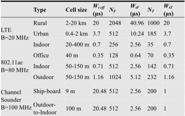
(2) According to the considered environment, Table 1 sum-marizes some useful parameters.
Table 1. Simulator parameters.
Type Cell size Wt eff
(µs) NF WtF (µs) NT WtT (µs) LTE B=20 MHz Rural 2-20 km 20 2048 40.96 1000 20 Urban 0.4-2 km 3.7 512 10.24 185 3.7 Indoor 20-400 m 0.7 256 2.56 35 0.7 802.11ac B=80 MHz Office 40 m 0.35 128 0.64 70 0.35 Indoor 50-150 m 0.71 512 2.56 142 0.71 Outdoor 50-150 m 1.16 1024 5.12 232 1.16 Channel Sounder B=100 MHz Ship-board 9 m 20.48 512 2.56 200 1 Outdoor- to-Indoor 100 m 20.48 512 2.56 200 1 Wteff represents the time window of the MIMO impulse
responses. The number of samples computed for the fre-quency domain is given b y:
(3) and for the time domain by:
(4) where WtF is the closest value for Wteff which is imposed by
the size NF = 2n of the FFT modules.
2.1. Channel Models
Two channel models are considered to cover indoor and outdoor environments: the TGn channel models (indoor) and the LTE channel models (outdoor). Moreover, using the channel sounder realized at IETR, measured impulse re-sponses are obtained for specific environments: shipboard, outdoor-to-indoor.
2.1.1. TGn Channel Models
TGn channel models [8] have a set of 6 profiles, labeled A to F, which cover all the scenarios. Each model has a number of clusters. For example, model E has four clusters. Each
American Journal of Networks and Communications 2012, 1(1): 1-10 3
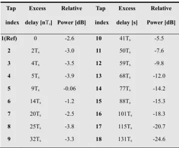
cluster corresponds to specific tap delays, which overlaps each other in certain cases. Table 2 summaries the relative power of the impulse responses for TGn channel model E by taking the Line-Of-Sight (LOS) impulse response as refer-ence [8]. The relative powers of all impulse responses for all TGn channel models are presented in [8]. According to the standard and the bandwidth, the sampling frequency is fs =
180 MHz and the sampling period is Ts = 1/fs.
Table 2. Simulator parameters.
Tap index Excess delay [nTs] Relative Power [dB] Tap index Excess delay [s] Relative Power [dB] 1(Ref) 0 -2.6 10 41Ts -5.5 2 2Ts -3.0 11 50Ts -7.6 3 4Ts -3.5 12 59Ts -9.8 4 5Ts -3.9 13 68Ts -12.0 5 9Ts -0.06 14 77Ts -14.2 6 14Ts -1.2 15 88Ts -15.3 7 20Ts -2.5 16 101Ts -18.3 8 25Ts -3.8 17 115Ts -20.7 9 32Ts -3.3 18 131Ts -24.6
The relative power of the first tap is different than zero because the impulse response is in Non-Line-Of-Sight (NLOS).
2.1.2. LTE Channel Models
LTE channel models are used for mobile wireless appli-cations. A set of 3 channel models is used to simulate the multipath fading propagation conditions. A detailed de-scription is presented in [9].
2.1.3. Measurement Data
The channel models used by the simulator can also be obtained from measurements by using a time domain MIMO channel sounder designed and realized at the IETR [10] and shown in Fig. 1.
The sounder uses a periodic pseudo binary sequence. It has 11.9 ns temporal resolution for 100 MHz bandwidth. The carrier frequencies are 2.2 GHz and 3.5 GHz.
Two measurement campaigns were carried out: The first campaign concerns a shipboard environment, while the second one considers an outdoor-to-indoor environment. The measured MIMO impulse responses are used thereafter by the hardware simulator.
For the shipboard measurement campaign [21] at 2.2 GHz, a Uniform Linear antenna Array (ULA) and a Uniform Rectangular antenna Array (URA) were used for the trans-mitter (Tx) and the receiver (Rx) respectively, to characterize the double directional channel on a 120o beam width in the horizontal plan.
For the outdoor-to-indoor measurements [22] at 3.5 GHz,
it has been shown that the penetration of electromagnetic waves mainly occurs through openings like doors and windows. Thus, a receiver located inside a building receives signals coming from few main directions. Two UCA (Uni-form Circular Array) were developed to characterize 360° azimuthal double directional channel at both link sides.
Figure 1. MIMO channel sounder: receiver and transmitter..
2.2. Proposed Scenario
The proposed scenario covers indoor environments at different environmental speeds. They consider the move-ments from an environment to another using an 802.11ac signal which has a 180 MHz sampling frequency (fs) at a
central frequency of 5 GHz.
A person moves from an office environment to a large indoor environment, then to an outdoor environment. For this scenario, the TGn channel model B, C and E cover the entire channel. Thus, three environments in this scenario are considered.
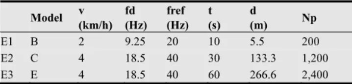
Fig. 2 and Table 3 present the scenario and the movement of the person in it.
Figure 2. Proposed scenario. E3
E1
Table 3. Scenario descriptions
Model v (km/h) fd (Hz) fref (Hz) t (s) d (m) Np E1 B 2 9.25 20 10 5.5 200 E2 C 4 18.5 40 30 133.3 1,200 E3 E 4 18.5 40 60 266.6 2,400
v is the mean environmental speed, fd is the Doppler
fre-quency, fref is the refresh frequency between two successive
MIMO profiles, t is the time duration of movements in the considered environment, d is the distance traveled and Np = t×fref is the number of profiles in each environment. fd is
equal to:
(5) where c is the celerity. fref is chosen > 2.fd to respect the
Nyquist-Shannon sampling theorem.
2.3. Time-Varying 2×2 MIMO Channel
In this section, we present the method used to obtain a model of a time variant channel, using the Rayleigh fading. A 2×2 MIMO Rayleigh fading channel [23-24] is consid-ered. The MIMO channel matrix H can be characterized by two parameters:
1) The relative power Pc of constant channel components
corresponds to LOS paths.
2) The relative power Ps of the channel scattering
com-ponents corresponds to NLOS paths. The ratio Pc/Ps is called Ricean K-factor.
Assuming that all the elements of the MIMO channel matrix H are Rice distributed, it can be expressed for each tap by:
(6) where HF and HV are the constant and the scattered channel
matrices respectively.
The total relative received power is P = Pc + Ps.
There-fore:
(7) (8) If we replace Equation (7) and Equation (8) in Equation (6) we obtain:
(9) To obtain a Rayleigh fading channel, K is equal to zero, so
H can be written as:
(10)
P is the relative power of the impulse response. It is
de-rived from Table 2 for each tap. For 2 transmit and 2 receive antennas:
(11) where Xij (i-th receiving and j-th transmitting antenna) are
correlated zero-mean, unit variance, complex Gaussian random variables as coefficients of the variable NLOS (Rayleigh) matrix HV.
To obtain correlated Xij elements, a product-based model
is used [23]. This model assumes that the correlation coef-ficients are independently derived at eac end h of the link:
(12)
Hw is a matrix of independent zero mean, unit variance,
complex Gaussian random variables. Rr and Rt are the
re-ceive and transmit correlation matrices. They can be written by:
(13) where is the correlation between channels (between their average signal gain) at two receives antennas, but originat-ing from the same transmit antenna (SIMO). It is the corre-lation between channels that have the same Angle of De-parture (AoD). is the correlation coefficient between channels at two transmit antennas that have the same receive antenna (MISO).
The use of this model has two conditions:
1) The correlations between channels at two receive (resp. transmit) antennas are independent from the Rx (resp. Tx) antenna.
2) If s1 (resp. s2) is the cross-correlation between
anten-na AoD esp. AoA) at the sa e side of the link, then: s1 = + an s2 = + .
s (r m
d
and are expressed by :
(14) where D = 2 d/λ, d = 0.5λ is the distance between two successive antennas, λ is the wavelength and Rxx and Rxy are
the real and imaginary parts of the cross-correlation function of the co idered cons rrelated angles:
cos sin (15)
sin sin (16)
The PAS (Power Angular Spectrum) closely matchs the Laplacian distribution [25-26]:
(17) where is the standard deviation of the PAS.
3. Architecture and Implementation on
FPGA
American Journal of Networks and Communications 2012, 1(1): 1-10 5
architectures are presented and implemented on a FPGA Virtex-IV.
3.1. Frequency Domain Architecture
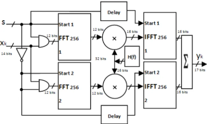
The new frequency architecture for a SISO channel is presented in Fig. 3. This architecture has been verified and tested with Gaussian impulse response and a description is presented in [27]. It operates correctly for signals with a number of samples exceeding the size of the FFT module.
Figure 3. Frequency architecture for a SISO channel for TGn channel
model E.
In general, for each SISO channel, the size of the FFT/IFFT modules is determined by the last excess delay of the impulse response of the channel. However, by simulating a scenario all the channels have to be considered. The highest last excess delay for the three environments is for E3
(Model E).
For TGn channel model E, Neff = 131 samples. Thus, N =
128 samples (the last tap has a relative power of -24.6 dB, therefore it will be considered as zero). However, to test the new architecture, it is mandatory to extend each partial input of N samples with a “tail” of N null samples, as in [27], to avoid a wrong result. Therefore, 256-FFT/IFFT modules are used.
H is the representation of h in the frequency domain. It
can be calculated by:
(18) where hq is h quantified on 16 bits and Wq i computs ed by:
(19)
where
(20) and each w l is quantified on 12 bits (which is the best trade-off between the occupation on FPGA of the FFT block and its accuracy).
The truncation block is located at the output of the digital adder. It is necessary to reduce the number of bits after the sum of the signals computed by the IFFT blocks to 14 bits. Thus, these samples can be accepted by the digital-to-analog converter (DAC), while maintaining the highest accuracy.
The immediate solution is to keep the most significant 14 bits. It is a “brutal” truncation. This truncation decreases the real value of the quantified output sample. 17 - 14 = 3 bits will be eliminated. Thus, instead of an output sample y, we
obtain , where is the biggest integer number
smaller or equal to u. However, for low voltages of the output of the digital adder, the brutal truncation generates zeros to the input of the DAC.
Therefore, a better solution is the sliding window trunca-tion presented in Fig. 4 which uses the 14 most effective significant bits. This solution modifies the output sample values. Therefore, the use of a reconfigurable amplifier after the Digital-Analog convertor must be used to restore the correct output value.
Figure 4. Sliding window truncation from 17 to 14 bits.
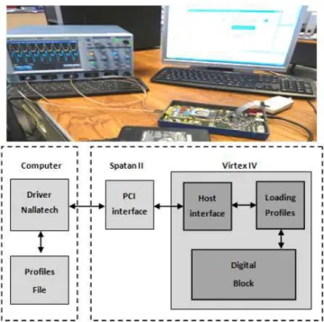
In order to implement the hardware simulator, the adopted solution uses a prototyping platform (XtremeDSP Devel-opment Kit-IV for Virtex-IV) from Xilinx [5], which is presented in Fig. 5 and described in [27].
Figure 5. XtremeDSP Development board Kit-IV for Virtex-IV.
The simulations and synthesis are made with Xilinx ISE [5] and ModelSim software [28].
The V4-SX35 utilization summary for this architecture with FFT 256 and IFFT 256 blocks is given in Table 4.
Table 4. Virtex-IV utilization for MIMO 2×2 frequency domain architecture
Number of slices Number of bloc RAM
14,755 out of 15,360 72 out of 192
96 % 37 %
Number of DSP48s 8 out of 192 4 %
3.2. Time Domain Architecture
In general, for each channel the FIR width and the number of used multipliers are determined by the taps of each channel. However, by simulating a scenario all the channels
have to be considered. To use limited number of multipliers on the FPGA and to switch from one environment to another, a solution is proposed to control the change of delays in architecture by connecting each multiplier block of the FIR by the corresponding shift register block. Therefore, the number of multipliers in the FIR filters is equal to the maximum number of taps between all channels of all envi-ronments. E3 has the highest number of taps which is 18.
Therefore, 4 FIR filters with 18 multipliers each are con-sidered. For TGn channel model E, the length of the FIR filter is N = 131. Thus, the ou put ignal can be cot s mputed as:
(21)
Figure 6. FIR 131 with 18 multipliers
The index q suggests the use of quantified samples and
hq(ik) is the attenuation of the kth path with the delay ikTs. Fig.
6 presents the architecture of the FIR filter 131 with 18 non-null coefficients. This architecture uses series of im-pulse responses with a refresh frequency fref depending on
the coherence time of the channel, in order to simulate a time variant channel. Therefore, we have developed our own FIR filter instead of using Xilinx MAC FIR filter to make it possible to reload the FIR filter coefficients. fref must be at
least twice the maximum Doppler frequency.
Table 5 shows the device utilization for four FIR filter 131 for 18 selected positions for the channel impulse response which are considered as non-null, in one V4-SX35 after synthesis, mapping and route.
Table 5. Virtex-IV utilization for MIMO 2×2 time domain architecture
Number of slices Number of bloc RAM
6,124 out of 15,360 72 out of 192 43 % 37 % Number of DSP48s 72 out of 192 37 % 3.3. ASF Solution
After analyzing the SNR (shown in Section 4.2.1), we
conclude that it is high only for high values of the input signals. Therefore, to decrease the error, a solution is pro-posed.
The input and output signals are limited to [-Vm,Vm] with Vm = 1 V. The solution consists on multiplying each sample
of the input signal with a corresponding 2k where k is an integer verifying: 0.5 < 2k.x < 1. However, we cannot predict x and multiply each sample by ASF at a high sample
fre-quency. Therefore we will use the ASF on the MIMO im-pulse responses. If hmax = max (|h|) < 0.5 it will be multiplied
by where is the unique integer verifying 0.5 <
.hmax < 1. In the case of a brutal truncation, ASF=2k.
However, for sliding truncation, if the output signals are presented on more than 14 bits, the sliding factor has to be considered to amplify the output signal in order to obtain the correct result. In this case, ASF = - . The ASF is sent to a reconfigurable analog amplifier to restore the true value of the output signals. ASF can be presented on 14 bits (limited by the D/A convertor). The first bit is “1” if it is a multiplication by ASF, and “0” if it is a division by ASF.
4. Results and Accuracy
4.1. Data Transfer Description
The channel impulse responses are stored on the hard disk of the computer and read via the PCI bus and then stored in the FPGA dual-port RAM.
Fig. 7 shows the connection between the computer and the FPGA board to reload the coefficients. The successive profiles are considered for the test of a 2×2 MIMO time-varying channel.
Figure 7. Connection between the computer and the XtremeDSP board..
The maximum data transfer of the impulse responses is: 18 × 4 = 72 words of 16 bits = 144 bytes to transmit for a
American Journal of Networks and Communications 2012, 1(1): 1-10 7
MIMO profile, which is: 144 × fref (Bps). fref depends on
each environment in the scenario. For E1 it is 2.88 (kBps)
and for E2 and E3 it is 5.76 (kBps).
The MIMO profiles are stored in a text file on the hard disk of a computer. This file is then read to load the memory block which will supply RAM blocks on the simulator (one block for each tap of the impulse response).
Reading the file can be done either from USB or PCI in-terfaces, both available on the used prototyping board. The PCI bus is chosen to load the profiles. It has a speed of 30 (MB/s). In addition, this is a bus of 32 (bits). Thus, on each clock pulse two samples of the impulse response are trans-mitted.
The Nallatech driver in Fig. 7 provides an IP sent directly to the "Host Interface" that reads it from the PCI bus and stores these data in a FIFO memory. The module called "Loading profiles" reads and distributes the impulse re-sponses in "RAM" blocks.
While a MIMO profile is used, the following profile is loaded and will be used after the refresh period.
4.2. Accuracy
In order to determine the accuracy of the digital block, a comparison is made between the theoretical and the Xilinx output signals.
A Gaussian input signal x(t) is considered long enough (more than N = 256 samples) to be used in streaming mode. To simplify the calculation, we consider x1(t) = x2(t)=x(t)
given by:
(22) where N = 256, Wt = NTs, mx = 3Wt/4 and σ = mx/4.
The A/D and D/A convertors of the development board have a full scale [-Vm,Vm], with Vm = 1 V. For the simulations
we consider xm = Vm/2.
The theor iet c o tput si na a e calculated byu g ls r :
(23)
(24)
4.2.1. Relative Error and SNR
The relative error is computed for each output sample by: (25) where YXilinx and Ytheory are vectors containing the samples of
corresponding signals. The Sign -to-N se Ral oi atio (SNR) is: (26)
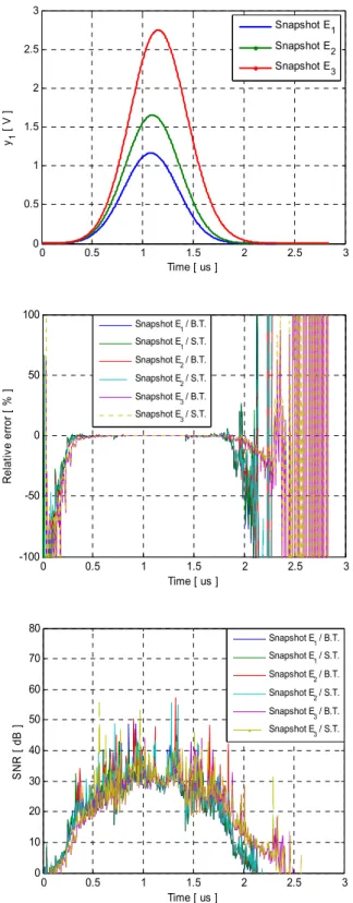
Fig. 8 shows a snapshot of the Xilinx output signal y1
(which is the first output for a MIMO 2×2) with their relative error and SNR using the new frequency architecture for E1, E2 and E3.
Figure 8. Snapshot of y1 with the relative error and SNR using the
fre-quency domain architecture.
The results are given with brutal truncation (B.T.) and sliding truncation (S.T.). Fig. 9 shows a snapshot of the
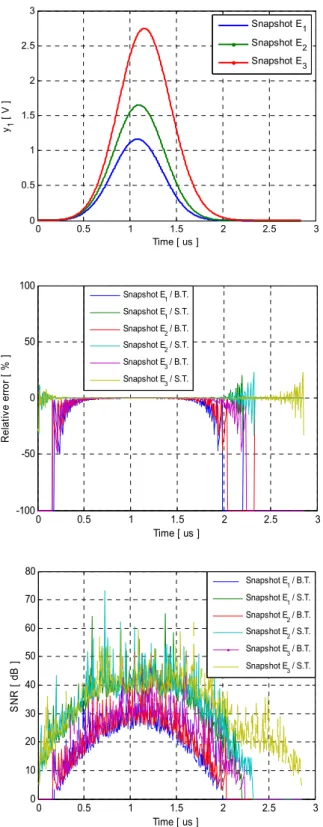
0 0.5 1 1.5 2 2.5 3 0 0.5 1 1.5 2 2.5 3 Time [ us ] y1 [ V ] Snapshot E 1 Snapshot E 2 Snapshot E 3 0 0.5 1 1.5 2 2.5 3 -100 -50 0 50 100 Time [ us ] R e la ti v e e rro r [ % ] Snapshot E 1 / B.T. Snapshot E 1 / S.T. Snapshot E 2 / B.T. Snapshot E 2 / S.T. Snapshot E 3 / B.T. Snapshot E 3 / S.T. 0 0.5 1 1.5 2 2.5 3 0 10 20 30 40 50 60 70 80 Time [ us ] S N R [ d B ] Snapshot E 1 / B.T. Snapshot E 1 / S.T. Snapshot E 2 / B.T. Snapshot E 2 / S.T. Snapshot E 3 / B.T. Snapshot E 3 / S.T.
Xilinx output signal y1 with their relative error and SNR
using the time domain architecture for E1, E2 and E3.
Figure 9. Snapshot of y1 with the relative error and SNR using the time
domain architecture.
4.2.2. Mean Global Relative Error and Global SNR with Time-Varying Profiles
The global values of the relative error and of the SNR
computed for the output signal before and after the final truncations are necessary to evaluate the accuracy of the architecture. The global relative e orr r is computed by:
(27) The global SNR is computed b : y
(28) where E = YXilinx - Ytheory is the error vector.
For a given vector X = [x1, x2,… x, L] | || is: , | x
(29) Table 6 shows the mean global values of the relative error and the SNR for all profiles using the two architectures. The results are given with sliding truncation and using ASF.
Table 6. Mean global error and SNR for the proposed scenario.
Frequency Architecture Time Architecture
Environment Error (%) SNR (dB) Error (%) SNR (dB)
E1 0.9241 40.68 0.0120 78.41
E2 0.3912 48.15 0.0101 79.91
E3 0.2427 52.29 0.0118 78.56
To compare the time domain architecture with the new frequency domain architecture, three points resume the comparison: the precision, the occupation on the FPGA and the latency.
With sliding window truncation, the relative error do not exceed 1 % (for the worst case, with TGn model B), which is sufficient for the test. However, the time domain architecture presents high precision.
In terms of occupation of slices on the FPGA Virtex-IV, the occupation for the time domain architecture is 43 % in contrast with the occupation of the frequency domain ar-chitecture which is 96 %. Thus, the time domain arar-chitecture presents another advantage. Moreover, with the time domain architecture we can simulate up to 8 SISO channels. Therefore, MIMO 4×2 system can be used and which oper-ates via 18×8 = 144 multipliers and producing an occupation of 87 % of slices on the FPGA.
In term of latency, the time domain architecture presents another advantage by generating a latency of 165 ns. How-ever, the new frequency architecture generates 7 s.
Therefore, the time domain architecture is more efficient to use, especially for MIMO systems. However, the use of more performing FPGAs as Virtex-VII is mandatory to solve the occupation problem for the new frequency domain architecture and to simulate high order MIMO systems.
5. Conclusion
This paper presents a frequency domain and time domain
0 0.5 1 1.5 2 2.5 3 0 0.5 1 1.5 2 2.5 3 Time [ us ] y1 [ V ] Snapshot E 1 Snapshot E 2 Snapshot E 3 0 0.5 1 1.5 2 2.5 3 -100 -50 0 50 100 Time [ us ] R e la ti v e e rro r [ % ] Snapshot E 1 / B.T. Snapshot E 1 / S.T. Snapshot E 2 / B.T. Snapshot E 2 / S.T. Snapshot E 3 / B.T. Snapshot E 3 / S.T. 0 0.5 1 1.5 2 2.5 3 0 10 20 30 40 50 60 70 80 Time [ us ] S N R [ d B ] Snapshot E1 / B.T. Snapshot E1 / S.T. Snapshot E2 / B.T. Snapshot E 2 / S.T. Snapshot E3 / B.T. Snapshot E3 / S.T.
American Journal of Networks and Communications 2012, 1(1): 1-10 9
architectures for the digital block of a hardware simulator of MIMO propagation channels. This simulator is used for WLAN 802.11ac applications. It characterizes an indoor scenario using TGn channel models. After the description of the general characteristics of the hardware simulator, the new architectures of the digital block have been presented and designed on a Xilinx Virtex-IV FPGA. Their accuracy, occupation on the FPGA and latency have been analyzed.
After a comparative study, in order to reduce occupation on the FPGA, the error and the latency of the digital block, the time domain architecture present the best solution for indoor environments.
For our future work, simulations made using a Virtex-VII [5] XC7V2000T platform will allow us to simulate up to 300 SISO channels. In parallel, measurement campaigns will be carried out with the MIMO channel sounder realized by IETR to obtain the impulse responses of the channel for specific and various types of environments. The final ob-jective of these measurements is to obtain realistic MIMO channel models in order to supply the hardware simulator. A graphical user interface will also be designed to allow the user to reconfigure the simulator parameters.
Acknowledgements
The authors would like to thank the “Région Bretagne” for its financial support of this work, which is a part of PALMYRE-II project.
References
[1] Wireless Channel Emulator, Spirent Communications, 2006.
[2] Baseband Fading Simulator ABFS, Reduced costs through baseband simulation, Rohde & Schwarz, 1999.
[3] A. S. Behbahani, R. Merched, and A. Eltawil, “Optimiza-tions of a MIMO relay network,” IEEE, vol. 56, no. 10, pp. 5062–5073, Oct. 2008.
[4] B. A. Cetiner, E. Sengul, E. Akay, and E. Ayanoglu, “A MIMO system with multifunctional reconfigurable anten-nas,” IEEE Antennas Wireless Propag. Lett., vol. 5, no. 1, pp. 463–466, Dec. 2006.
[5] "Xilinx: FPGA, CPLD and EPP solutions", www.xilinx.com.
[6] P. Murphy, F. Lou, A. Sabharwal, P. Frantz, "An FPGA Based Rapid Prototyping Platform for MIMO Systems", Asilomar Conf. on Signals, Systems and Computers, ACSSC, vol. 1, pp. 900-904, 9-12 Nov. 2003.
[7] P. Murphy, F. Lou, J. P. Frantz, "A hardware testbed for the implementation and evaluation of MIMO algorithms", Conf. on Mobile and Wireless Communications Networks, Singa-pore, 27-29 Oct. 2003.
[8] V. Erceg et al., “TGn Channel Models”, IEEE 802.11- 03/940r4, May 10, 2004.
[9] Agilent Technologies, “Advanced design system – LTE
channel model - R4-070872 3GPP TR 36.803 v0.3.0”, 2008.
[10] G. El Zein, R. Cosquer, J. Guillet, H. Farhat, F. Sagnard, “Characterization and modeling of the MIMO propagation channel: an overview” European Conference on Wireless Technology, ECWT, 2005.
[11] H. Farhat, R. Cosquer, G. El Zein, "On MIMO channel characterization for future wireless communication systems", 4G Mobile & Wireless Comm.Tech., River Publishers, Aal-borg, Denmark, 2008.
[12] S. Picol, G. Zaharia, D. Houzet and G. El Zein, "Hardware simulator for MIMO radio channels: Design and features of the digital block", Proc. of IEEE VTC-Fall 2008, Calgary, Canada, 2008.
[13] S. Picol, G. Zaharia, D. Houzet and G. El Zein, "Design of the digital block of a hardware simulator for MIMO radio channels", IEEE PIMRC, Helsinki, Finland, 2006.
[14] D. Umansky, M. Patzold, "Design of Measurement-Based Stochastic Wideband MIMO Channel Simulators", IEEE Globecom, Honolulu, Hawai, 30 Nov. - 4 Dec. 2009.
[15] H. Eslami, S.V. Tran and A.M. Eltawil, "Design and imple-mentation of a scalable channel Emulator for wideband MIMO systems", IEEE Trans. on Vehicular Technology, vol. 58, no. 9, pp. 4698-4708, Nov. 2009.
[16] S. Fouladi Fard, A. Alimohammad, B. Cockburn, C. Schle-gel, "A single FPGA filter-based multipath fading emulator", VTC-Fall, Canada, 2009.
[17] B. Habib, G. Zaharia, G. El Zein, “MIMO hardware simu-lator: digital block design for 802.11ac applications with TGn channel model test”, IEEE VTC Spring, Yokohama, Japan, May 2012.
[18] B. Habib, G. Zaharia, G. El Zein, “Hardware simulator: Digital block design for time-varying MIMO channels with TGn model B test”, IEEE ICT, Lebanon, April 2012.
[19] B. Habib, G. Zaharia, G. El Zein, “Digital block design of MIMO hardware simulator for LTE applications”, IEEE ICC, Ottawa, Canada, June 2012.
[20] A. Damnjanovic, et al., “A survey on 3GPP heterogeneous networks”, IEEE Wireless Communications, Qualcomm inc., June 2011.
[21] B. Habib, H. Farhat, G. Zaharia, G. El Zein, “Hardware Simulator Design for MIMO Propagation Channel on Ship-board at 2.2 GHz”, Journal of Wireless Personal Communi-cations, 2012, doi: 10.1007/s11277-012-0954-2.
[22] B. Habib, H. Farhat, G. Zaharia, G. El Zein, “MIMO Hard-ware Simulator Using Standard Channel Models and Meas-urement Data at 2.2 and 3.5 GHz”, Journal of Communica-tion and Computer, 2013, JCC- E20121101-3.
[23] W. C. Jakes, “Microwave mobile communications”, Wiley & Sons, New York, Feb. 1975.
[24] J. P. Kermoal, L. Schumacher, K. I. Pedersen, P. E. Mogensen, F. Frederiksen, “A stochastic MIMO radio channel model with experimental validation”, IEEE Journal on Selected Areas of Commun., Vol. 20, No. 6, Aug. 2002, pp. 1211-1226.
angle of arrival characteristics of an indoor environment”, IEEE J. Select. Areas Commun., Vol. 18, No. 3, March 2000, pp. 347-360.
[26] C-C. Chong, D. I. Laurenson, S. McLaughlin, “Statistical Characterization of the 5.2 GHz wideband directional indoor propagation channels with clustering and correlation proper-ties”, in proc. IEEE Veh. Technol. Conf., Vol. 1, Sept. 2002,
pp. 629-633.
[27] B. Habib, G. Zaharia and G. El Zein, "Improved Frequency Domain Architecture for the Digital Block of a Hardware Simulator for MIMO Radio Channels", IEEE 978-1-61284-943-0, ISSCS June 2011.
[28] “ModelSim - Advanced Simulation and Debug-ging”, http://model.com.