HAL Id: hal-03105414
https://hal.archives-ouvertes.fr/hal-03105414
Submitted on 11 Jan 2021HAL is a multi-disciplinary open access archive for the deposit and dissemination of sci-entific research documents, whether they are pub-lished or not. The documents may come from teaching and research institutions in France or abroad, or from public or private research centers.
L’archive ouverte pluridisciplinaire HAL, est destinée au dépôt et à la diffusion de documents scientifiques de niveau recherche, publiés ou non, émanant des établissements d’enseignement et de recherche français ou étrangers, des laboratoires publics ou privés.
TiO 2 –SiO 2 nanocomposite thin films deposited by
direct liquid injection of colloidal solution in an O 2
/HMDSO low-pressure plasma
Maria Mitronika, Jacopo Profili, Antoine Goullet, Nicolas Gautier, Nicolas
Stephant, Luc Stafford, Agnès Granier, Mireille Richard-Plouet
To cite this version:
Maria Mitronika, Jacopo Profili, Antoine Goullet, Nicolas Gautier, Nicolas Stephant, et al.. TiO 2 –SiO 2 nanocomposite thin films deposited by direct liquid injection of colloidal solution in an O 2 /HMDSO low-pressure plasma. Journal of Physics D: Applied Physics, IOP Publishing, 2021, 54 (8), pp.085206. �10.1088/1361-6463/abc84d�. �hal-03105414�
1
TiO
2
-SiO
2
Nanocomposite thin films deposited by
1
Direct Liquid Injection of colloidal solution in an
2
O
2
/HMDSO low-pressure plasma
3
Maria Mitronika1, Jacopo Profili2, Antoine Goullet1, Nicolas Gautier1, Nicolas Stephant1,
4
Luc Stafford2, Agnès Granier1, Mireille Richard-Plouet1*
5
1 Université de Nantes, CNRS, Institut des Matériaux Jean Rouxel, IMN, F-44000 Nantes,
6
France
7
2 Département de physique, Université de Montréal, 1375 Avenue Thérèse-Lavoie-Roux,
8
Montréal, Québec, H2V 0B3, Canada
9
*corresponding author: Mireille.Richard@cnrs-imn.fr
10
Keywords: low-pressure plasma processing, direct-liquid injection, colloidal solution, TiO2
11
nanoparticles, TiO2-SiO2 nanocomposite thin films
12
Abstract: TiO2 nanoparticles (NPs), 3 nm in size, were injected inside a very-low-pressure O2
13
plasma reactor using a liquid injector and following an iterative injection sequence.
14
Simultaneously, hexamethyldisiloxane (HMDSO) vapor precursor was added to create a SiO2
15
matrix and a TiO2-SiO2 nanocomposite (NC) thin film. Both the liquid injection and vapor
16
precursor parameters were established to address the main challenges observed when creating
17
NCs. In contrast to most aerosol-assisted plasma deposition processes, Scanning/Transmission
18
Electron Microscopy (S/TEM) indicated isolated (i.e. non-agglomerated) NPs distributed in a
19
rather uniform way in the matrix. The fraction of the TiO2 NPs inside the SiO2 matrix was
20
estimated by SEM, Spectroscopic Ellipsometry (SE), and X-ray Photoelectron Spectroscopy.
21
All techniques provided coherent values, with percentages between 12 and 19%. Despite the
22
presence of TiO2 NPs, SE measurements confirmed that the plasma-deposited SiO2 matrix was
23
dense with an optical quality similar to the one of thermal silica. Finally, the percentage of TiO2
24
NPs inside the SiO2 matrix and the effective refractive index of the NCs can be tuned through
25
judicious control of the injection sequence.
26
2 1. Introduction
28 29
Nowadays, there is an ongoing demand for smaller, faster, and low-cost integrated
30
systems. Achieving this often requires new materials and structures that combine the more
31
conventional ones. In this context, nanocomposite (NC) thin films formed of nanoobjects
32
embedded in a matrix have gained great attention, as the properties of the resulting composite
33
may be more likely to resemble those of the interface zones rather than those of the original
34
constituents[1]. The high surface-area-to-volume ratio in NCs can also lead to enhanced
35
macroscopic properties compared to the bulk materials.
36 37
One of the most significant challenge in the development of NC thin films is the control
38
of the growth mechanisms, the final morphology and the incorporation of the nanoobjects
39
using reproducible, versatile and low-cost processes. Several chemical and physical methods
40
have been used in recent years. For example, sol-gel is a well-established process based on
41
hydrolysis and condensation reactions.[2,3] The main drawback of this approach is the need
42
of several steps to produce NC thin films. In addition, the toxicity of the nanoparticles (NPs)
43
during the drying of the film[4] limits the industrialization. Vacuum processes such as
44
PECVD or CVD have also demonstrated their ability to synthesize NC thin films by
45
controlling the plasma- or thermally-activated reaction pathways.[5,6] In parallel, sputtering
46
approaches have also been used to create metal, metal-oxide or metal-nitrides NC thin films.
47
[4,7]
48 49
Recently, there have been some attempts using hybrid (aerosol-assisted, direct liquid
50
injection etc.) approaches for the creation of NC thin films. Profili et al. [8] implemented a
51
one-step approach for the deposition of ZnO-SiO2 NC coatings on wood by the atomization
52
of a stable suspension of ZnO dispersed in hexamethyldisiloxane (HMDSO) in an
53
atmospheric pressure dielectric barrier discharge (DBD). Ross et al.[9] elaborated composite
54
films using an ultrasonic atomizer and a PECVD system using Tetraethoxysilane (TEOS) as
55
a matrix precursor and polystyrene nanoparticles with a mean size of 96 nm. The pressure in
56
the specific system was varied between 100 and 500 mTorr. More recently, Kahn et al.[10]
57
proposed a new method that allowed to synthesize NPs from organometallic precursor in a
58
reactor-injector prior to their injection in a RF low-pressure plasma reactor at 750 mTorr. The
59
resulted NC thin films consisted of small (6 ± 3 nm) and isolated ZnO NPs homogeneously
60
dispersed in an amorphous hydrogenated carbon matrix. This increased interest in hybrid
61
approaches led to the development of new direct liquid injection systems[11] and studies
62
regarding the interactions of the liquid droplets with the low pressure plasma systems [12]
63
(misty plasmas). As a general trend, most of these studies focus on the deposition of inorganic
64
NPs-organic matrix NC film. The majority of the reposted works involve high-pressure and
65
atmospheric-pressure plasma system. These systems have been thoroughly studied mainly
66
because of the technically-challenging conditions existing at very low pressures (e.g. risk of
67
contamination of the vacuum chamber, malfunction of the turbomolecular pump, fast liquid
68
vaporization without reaching the substrate).[13,14] In most cases, however, the NPs in NC
69
thin films are agglomerated, and their size is increased compared to the one in the colloidal
70
solution before their injection in the plasma. [13,15–22]
3
The main bottlenecks for producing NC thin films are incorporating a high-volume fraction,
72
preventing the agglomeration of NPs and dispersing them homogeneously in the matrix. Using
73
a very-low-pressure system, the objective is to deposit thin films incorporating 3-nm TiO2 NPs
74
in a high-quality inorganic SiO2 matrix. This is accomplished by the direct liquid injection of
75
the 3-nm TiO2 NPs colloidal solution without a carrier gas and the addition of HMDSO vapor
76
precursor in the very-low-pressure O2 plasma. Furthermore, as several works involving
77
atmospheric-pressure plasma systems reported challenges to deposit in one-step and acquire
78
good quality NC films, the differences and prospects in using very-low-pressure hybrid systems
79
is investigated. The evaluation of the NC’s quality, homogeneity and distribution of the TiO2
80
NPs are achieved by various characterization techniques such as high-resolution Scanning
81
Transmission Electron Microscopy (HR-STEM), Energy Dispersive X-ray spectrometry
82
(EDX), Atomic Force microscopy (AFM) and X-ray photoelectron spectroscopy (XPS).
83
Finally, with this work, besides establishing this novel and versatile approach, the objective is
84
to identify experimental conditions for acquiring thin films oriented towards optical
85
applications. Therefore, the optical characteristics of the film, such as its effective refractive
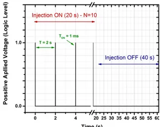
86
index, are being extracted with Spectroscopic Ellipsometry (SE).
87 88
2. Experimental Details 89
90
2.1 TiO2 NPs colloidal solution
91 92
The colloidal solution used for the injection of the TiO2 NPs in the very-low-pressure plasma
93
has been synthesized following a specific protocol developed at the Institut des Matériaux Jean
94
Rouxel.[23,24] The NPs enclosed in the colloidal solution were well-defined and
95
monodispersed with an anatase crystalline structure. Their mean hydrodynamic diameter
96
(including species of the solvent surrounding the NPs to counterbalance surface charge)
97
obtained by Dynamic Light Scattering (DLS) with Zetasizer NanoZS (Malvern) was centered
98
on 3.7 nm (Figure 1). The double layer surrounding the NPs has been estimated at 1 nm.[24]
99
Therefore, the actual TiO2 nanocrystallite diameter lay at 2.7 nm. As synthesized, the solvent
100
of this solution was a mixture of 4-methyl-1,3-dioxolan-2-one also known as propylene
101
carbonate (PC) and 1,2-propanediol or propylene glycol (PG), with a molar fraction of
102
27%:73% respectively. From previous studies of our group [23,25], we identified that some
103
solvent molecules remain attached to the surface of the NPs, creating an 4.7 Å hydroxylated
104
and organic shell around TiO2 NPs.
105 106
4 107
Figure 1: Hydrodynamic size distribution of the TiO2 NPs inside the as-prepared (PC-PG)
108
colloidal solution deduced from DLS. Line corresponds to a Log-Normal distribution fit, based
109
on which the mean diameter size was extracted.
110
For the effective injection and evaporation of the colloidal solution in the very-low-pressure
111
PECVD system, the dilution of the colloidal solution with a more volatile one was carried out.
112
Therefore, the final colloidal solution used was a mixture of PC:PG:Methanol with a volume
113
fraction of 20.25:54.75:25 . The size distribution of TiO2 NPs in the diluted solution was
114
verified with DLS and was not altered by either dilution or long-time storage..
115 116
2.2 Deposition of TiO2-SiO2 NC thin films using the hybrid approach
117 118
For the elaboration of the TiO2-SiO2 NC thin film, the colloidal solution was injected in a
119
very-low-pressure PECVD reactor. The schematic representation of the hybrid experimental
120
setup is given in Figure 2. The reactor comprises a very-low-pressure high-density Inductively
121
Coupled Plasma (ICP) source created at 13.56 MHz (400 W) in a fused silica discharge tube
122
using a helicon antenna which is also connected to a matching network. A static magnetic field
123
(50 G) is applied to the source in order to confine the electrons and densify the plasma. The
124
plasma then expands into a stainless-steel processing chamber where the substrate holder is
125
located. The substrate holder is 17 cm in diameter located in the middle of the processing
126
chamber with a distance of 16.8 cm from the bottom of the ICP antenna. The Si substrates used,
127
which were positioned in the middle of the substrate holder, were 1 cm x 2 cm in dimension
128
and their temperature was measured at 400 K through temperature-sensitive labels located at
129
the substrate’s backside. In this system, plasma gases (95% O2, 5% Ar here) are introduced at
130
the top of the plasma source and the high-vacuum pumping system is located 11 cm from the
131
bottom of the processing chamber. The outlet of the vacuum pumping system that includes also
132
a cold trap, is 10 cm in diameter. In Figure 2b, its location related to the substrate holder and
133
the liquid doser can be seen. More information about the reactor can be found in [26,27].
134 135
For the deposition of the SiO2 matrix, HMDSO vapor was introduced from a
heated-136
container (at 35.8 °C) without any carrier gas through a distribution ring (indicated with blue
137
in Figure 2), located 8 cm above the substrate. The injection of the TiO2 colloidal solution was
5
achieved through a separate industrial direct-liquid doser (indicated with red in Figure 2). It is
139
an injection system from Kemstream that features a normally closed fast solenoid valve (or
140
injector), with a small conductance (flow coefficient), commonly called Cv. This valve is
141
controlled in pulsed regime. The orifice of the injection system includes 8 holes with a diameter
142
of 70 µm each. This injection system was mounted on the PECVD reactor with an angle of 55°
143
with respect to the substrate holder. The distance of the injector to the reactor was fixed at 20
144
cm and therefore the distance of the injector to the substrate can be calculated at 48.24 cm. The
145
pipe connecting the injector to the reactor was heated (yellow lines indicating the heating wire
146
in Figure 2) at 423 K to enhance the evaporation process of the produced droplets.
147 148
149
Figure 2: Schematic of the hybrid experimental setup including the low pressure ICP O2
150
reactor, the liquid doser apparatus (with red) and the HMDSO vapor distribution system (with
151
bleu) at a) side view and b) top view. The in situ characterization techniques are also indicated
152
on this schematic.
153 154
For maintaining very-low pressure during the deposition (3 mTorr) and therefore obtaining
155
a high-quality inorganic matrix, no additional carrier gas has been used to assist the injection
156
of TiO2 NPs. In such conditions, the droplet creation and the formation of the aerosol were
157
mainly driven by the difference in pressure between the reservoir of the colloidal solution (760
158
Torr) and the plasma reactor (3 mTorr).[28] For this specific pressure difference, the mean
159
droplet size obtained by Phase Doppler Anemometry (PDA) was 65.0 µm with a standard
160
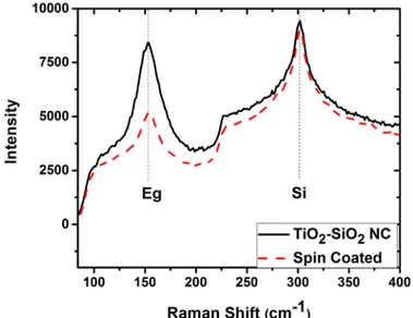
deviation of 29 µm. The opening of the injection valve was trigged by applying a positive pulse
161
controlled by the VapSoft software of the direct-liquid injector. It is worth highlighting that
162
during each pulsed injection of the colloidal solution in the plasma reactor the pressure
163
instantaneously increased from 3 to 15 mTorr due to solvent evaporation[12] and then returned
164
back to the steady-state pressure (3 mTorr) within less than 2 s. The pressure variation was
165
detected from the capacitance diaphragm gauge (MKS Instruments France SA) and was read
166
on the go. Additionally, the 15 mTorr was the maximum value that was provided by the gauge
167
reading. Upon injection and pressure increase, the intensity of the ICP O2 plasma is decreased
168
retrieving within less than 2 seconds its usual brightness. Despite this fact, the plasma is never
6
extinguished remaining ignited during the total duration of the process. As a matter of fact, the
170
intensities of O and Ar lines (at 394.5 nm and 419.8 nm, respectively) measured by time
171
resolved OES are supplied as Electronic Supporting Information (ESI). These results, indicate
172
that during each injection (within the DLI-ON), the emission intensities of the Ar and O lines
173
are decreased trying to retrieve their steady state value within the pulses (Figure S1). This
174
variation, especially for the Ar emission intensity is related to the pressure variation. Both
175
intensities never reach a zero value verifying once more that the plasma remains ignited during
176
the total duration of the hybrid deposition process. Regarding the RF power supply, during the
177
droplet injection, a reflected power with a mean value of 2 W is provided by the CESAR RF
178
Power Generator.
179 180
For deposition experiments, the total sequence length was set at one minute (Figure 2). More
181
specifically, during the first 20 s, N=10 pulses of 1 ms (TON =1 ms) were triggered each two
182
seconds (T=2 s). Thus, after this first-time lapse of N*2 s = 20 s, the valve remained closed for
183
60-N*2 s = 40 s (TOFF). Such sequence was repeated for 50 minutes. The solvent mass rate was
184
estimated at 2.33 mg per pulsed injection and therefore 23.3 mg per minute for N=10 cycles.
185
During this intermittent mode of injection (Figure 3), the oxygen mass flow rate of the working
186
gas was set at 24 SCCM (standard cubic centimeters per minute) while the continuous mass
187
flow rate of HMDSO vapor was maintained at 0.11 SCCM. The fraction between HMDSO and
188
O2 was chosen in a way to produce a silica-like matrix with a very low carbon content[29]. O2
189
was also used to ensure the removal of solvent-based organic moieties surrounding TiO2
190
NPs[30].
191 192
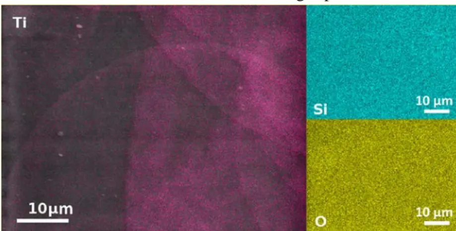
193
Figure 3: Description of the plasma deposition sequence including the first part of pulsed 194
injection of the colloidal solution (10 cycles of TON with an off time of 2 s between each pulse
195
for a total of 20 s) and the second part without liquid injection (for a total off time TOFF = 40s).
196
2.3 Characterization of the NC thin films 197
198
The cross section and distribution of the TiO2 NPs inside the SiO2 matrix were investigated
199
(Figure 4 a, b ,c) using transmission electron microscopy (S/TEM Themis Z G3, 300kV,
200
Thermo Fisher Scientific). A typical image of high-angle annular dark-field scanning
201
transmission electron microscopy (HAADF-STEM, 28.5 mrad, probe corrected) is reported in
7
Figure 4 d. The elemental mapping (Figure 4 e f g) was performed using EDX (energy
203
dispersive X-ray spectrometer) analysis. For the effective characterization of the samples
204
through TEM, the deposition was carried on Tin doped Indium oxide deposited on polyethylene
205
terephthalate (ITO (50 nm) / PET (125 µm), Sheldahl). Cross-sections of the sample were
206
prepared by using an ultramicrotome (Leica UC7/FC7) equipped with diamond knife
207
(Diatome). The morphological analysis of the TiO2-SiO2 NC film on Si was carried out through
208
Scanning Electron Microscopy (SEM) with a JEOL JSM 7600F, in a secondary electron mode,
209
operating at 5 kV. The chemical analysis by EDX was conducted with a SAMx SDD system
210
on a SEM JEOL JSM 5800LV. To increase the EDX signals, a dedicated thicker film was
211
prepared (224 nm). To ensure that no additional Si coming from the substrate would interfere
212
with the quantification of the silica matrix the dedicated thicker NC film was deposited on
213
ITO/PET substrate. To probe different thicknesses, EDX spectra were recorded at three
214
accelerating voltages: 15 kV, 10 kV and 7 kV and a magnification of X1000 (2552 µm2) was
215
chosen to smooth any local anomalies of chemical concentrations. The software Stratagem was
216
used for EDX measurements because first the volume irradiated by the electron beam and
217
second the X-ray collected are related to a larger depth than the thickness of the top layer. [31]
218
The atomic percentages were determined by considering a theoretical model for the probed
219
zone [32]. For this, three layers were considered: first, 224 nm of NC (Ti, Si, O), second, 50
220
nm of ITO (In, Sn, O), and third, PET (C, O). The different atomic percentages were fitted to
221
reproduce the intensity of EDX signals as a function of the accelerating voltage, accounting for
222
the thicknesses of the NC and ITO and attenuation of signals throughout the different layers.
223
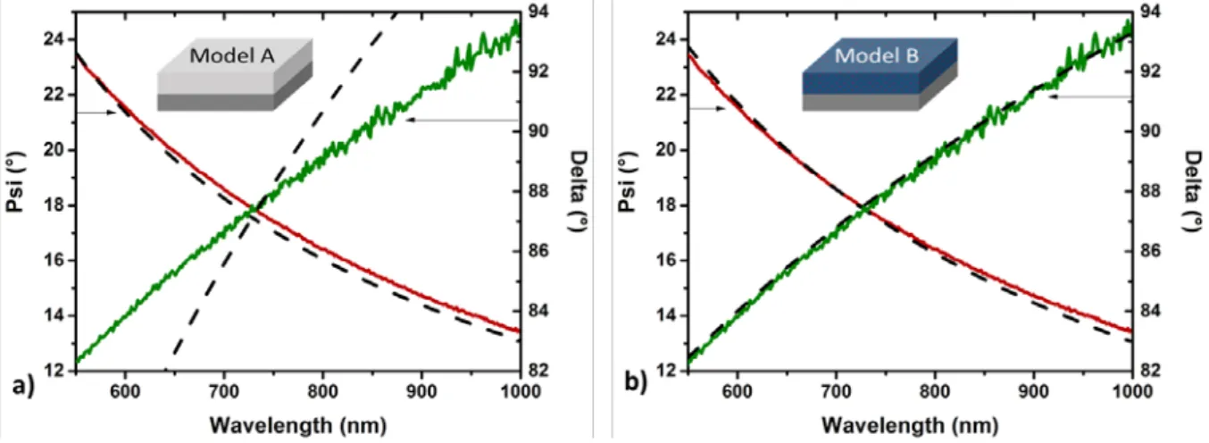
The determination of carbon and oxygen was not reliable because the corresponding signals
224
may come from ITO and PET underneath (one must also consider that the effective thickness
225
of PET analyzed by EDX depends on the accelerating voltage). However, the precautions taken
226
before acquisition and the good fit between theoretical curves generated by Stratagem and
227
experimental values make it possible to rely on the results concerning silicon and titanium
228
atomic percentages.
229 230
The optical characteristics and composition of the TiO2-SiO2 NC thin films deposited on
231
silicon substrates were also examined through a rotating compensator spectroscopic
232
ellipsometer (J.A. Woollam M-2000). The measurements were conducted in situ (i.e. during
233
plasma deposition) in the wavelength range of 245 to 1000 nm at 71.7° incident angle.
234 235
Atomic Force Microscopy (AFM) was used in tapping mode to investigate the nanostructured
236
topography and roughness of the NC thin films. AFM Nanowizard II (JPK Instruments),
Al-237
coated cantilever (PPP-NCHR-50 from NANOSENSORS) with a free resonance frequency of
238
330 kHz and a typical spring constant of about 42 N/m were used. The size distribution of the
239
NPs was deduced from the AFM scans by using the ImageJ software after adjustment of the
240
threshold and transformation in binary format.
241 242
Raman spectroscopy measurements were performed using a microconfocal Raman
243
microscope (Renishaw inVia). The instrument was equipped with a double edge filter to
244
eliminate the Rayleigh scattering and a charged couple device (CCD) camera working at a
245
temperature of 220 K with a 1024x256 pixel array. The setup was composed of a confocal
8
microscope that was equipped with an automated XYZ table and an X50 magnification
247
objective. The laser excitation source used was set at 514 nm and the focused power was
248
adjusted to avoid any degradation of the samples. Therefore, the power was fixed at 1.5mW
249
and a recording time of 1 s with an accumulation of 10 measurements was used.
250 251
The chemical characterization of the topmost surface was investigated with X-ray
252
photoelectron spectroscopy (XPS) on a Kratos Nova spectrometer with Al Kα radiation at
253
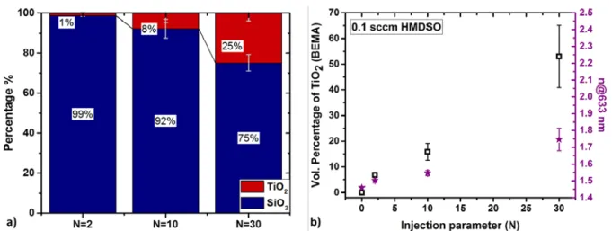
1486.6 eV. Neutralization of the surface was applied to avoid differential charging effect.
254
Survey spectra were measured from 1200 to -2 eV (Binding Energy) using a pass energy of 160
255
eV whereas high-resolution spectra over specific regions of interest were recorded with a pass
256
energy of 40 eV. Short time measurements were recorded (dwell of 100 ms per 0.1 eV
step-257
scan for O1s, Ti 2p and 200 ms for C1s). After checking that no X-ray damage was induced,
258
the scans were summed up to increase the signal-to-noise ratio. The decomposition and fitting
259
of the measured XPS peaks was carried out using CasaXPS software [33]. After accounting for
260
the background using a U2-Tougaard background, Gaussian-Lorentzian (30-70%) functions
261
were selected to model the different components. The signals were calibrated in energy
262
according to the position of the C 1s band at the binding energy of 285 eV.
263 264
To be able to compare the results obtained from different characterization techniques, detailed
265
calculations have been achieved (which are supplied as Electronic Supporting Information) to
266
transform at% of elements to vol% of oxides.
267 268
3. Results 269
270
3.1 Structural characterization of the TiO2-SiO2 NC thin films
271 272
Cross section structural analysis of the plasma-deposited NC thin film was performed using
273
TEM and STEM (Figure 4). Through multiple measurements on low magnification images (Fig.
274
4a), the thickness of the film was estimated at 85 +/- 6 nm (a growth rate of 1.7 nm/min for a
275
total plasma deposition time of 50 min). This value is comparable to the one achieved in
276
O2/HMDSO plasmas without injection of the TiO2 colloidal solution[29]. Using
high-277
resolution images on the rectangular area (black contour) shown in Fig. 4b and based on the
278
contrast between the amorphous matrix and the basal planes of the nanocrystals, some TiO2
279
NPs can be identified (enlarged NPs as an inset in Figure 4) and stressed with white-rounded
280
contour shapes (Figure 4c). Interestingly, no agglomeration of these NPs is observed but rather
281
an assembly of small and isolated TiO2 NPs in the SiO2 matrix. Using ImageJ software, the
282
size of each of these NPs (14 nanoparticles identified in the specific zone probed by electron
283
microscopy) was extracted and their mean value was found to be at 2.7 ± 0.4 nm. By comparing
284
this value with the hydrodynamic diameter of TiO2 NPs in the colloidal solution obtained by
285
DLS (2.7 nm + 1 nm, Figure 1), it can be confirmed that the NPs’ size remains intact following
286
the aerosol formation and plasma deposition. This is a remarkable result with respect to other
287
experiments on hybrid plasma deposition of NC thin films for which agglomeration phenomena
288
were deemed unavoidable[13,15–22]. Moreover, TiO2 NPs displayed in Figure 4c seem
289
dispersed in a rather random way in the SiO2 matrix, with no evidence of preferential
9
incorporation sites. No cracking of the SiO2 layers is visible, showing that the insertion of the
291
NPs does not strongly affect the growth of the silica layer.
292 293
The typical HAADF-STEM image given in the same figure confirms that no bright contrast
294
associated to possible agglomeration of the electronically denser TiO2 NPs is detected,
295
indicating the homogeneity of the NPs dispersion, at this scale of observation. Moreover, EDX
296
elemental mapping also confirms that both oxygen and silicon (Fig.4 e,f) are homogeneously
297
distributed along the cross section of the NC thin film. On the other hand, Ti (Fig. 4g) signal,
298
which is only linked to the TiO2 NPs, is identified with some small dots verifying the TEM
299
images (Fig. 4c) and their distribution inside the film. Since the data are a projection of 80 nm
300
thin sample, the reinforcement in contrast, (in some small parts of Fig.4g) may come from
301
particles distributed along this thickness.
302 303
304
Figure 4: TEM cross section of the TiO2-SiO2 NC thin film a) in low magnification indicated
305
with white dashed lines, b) high magnification and c) higher magnification image focusing on
306
the distributed TiO2 NPs inside the SiO2 matrix. An inset is given with higher magnification
10
focusing on the basal planes of the anatase nanoparticles. d) Typical HAADF-STEM image of
308
the SiO2-TiO2 NCs in a selective area. Elemental mapping for e) O, f) Si and g) Ti.
309
The crystalline phase of the TiO2 NPs was identified using Raman spectroscopy. Figure 5
310
presents the Raman spectra of the plasma-deposited NC thin film (black line) and the TiO2 NPs
311
spin coated thin films (red line) using the as synthesized colloidal solution, with a focus on the
312
Eg anatase peak. The analysis was limited to using the peak positions since extreme caution is
313
required when using the Raman intensities of very thin films. Raman modes can be assigned to
314
the Raman spectra of the anatase crystal:144 (Eg), 200 (Eg), 400 (B1g), 513 (A1g), 518 (B1g)
315
and 642 cm-1 (Eg) [34,35]. In this figure, it can be observed that the Eg peak lies at 154 cm-1, a
316
value shifted from the expected anatase peak at 144 cm-1 [36,37]. It is well-established
317
experimentally that Raman spectra of low-dimensional semiconductor crystals are modified
318
when compared to the one of bulk crystals: (1) the Raman peaks are asymmetrically broadened
319
and (2) their positions are shifted [38,39]. The former is not observed mainly due to the size
320
distribution of the specific nanocrystals. This effect, results in masking the confinement effect
321
and averaging the Raman response [40]. However, the results presented in Figure 5 (black line)
322
confirm the strong shift of the Eg band that the plasma-deposited TiO2 NPs embedded in the
323
SiO2 matrix are anatase crystallites and in nanometric size. In addition to this, the Raman
324
spectrum of the TiO2 NPs thin film through the spin-coated technique is given with red color.
325
The fact that for both cases the anatase peak is found in the same position (154 cm-1) confirms
326
that upon the colloidal solution dilution, the TiO2 NPs injection and the SiO2 matrix deposition,
327
the nano crystallite is not affected.
328 329
330
Figure 5: Raman spectra indicating the Anatase Eg band at 154 cm-1 and the second order Si
331
band peak at 303 cm-1 for the TiO
2-SiO2 NC thin film through the hybrid approach (black color)
332
and the spin coated TiO2 NPs thin film using the as synthesized colloidal solution.
333 334 335 336
3.2 Morphological analysis of the TiO2-SiO2 NC thin films
337 338
11
The surface morphological analysis of the TiO2-SiO2 NC thin film was investigated by SEM
339
and AFM as shown in Figure 6. From the SEM top view image (Fig. 6a) in high magnification,
340
the surface of the film is homogeneous and nanostructured, revealing some rounded domains.
341
Since the resolution of the SEM is at 10 nm, one can understand that the exact identification
342
and quantification of these domains is impossible. These same rounded domains are highlighted
343
in the AFM measurements (bright yellow-white color in Fig 6b). They are located higher on
344
the z axis and their size is higher than the one of the initial NPs in solution measured by DLS
345
in Figure 1. From detailed analysis of multiple AFM scans at low and high magnification, the
346
mean size of the domains was extracted and plotted as a histogram in Fig 6c. The fitting of a
347
LogNormal distribution provided a mean size of 23 nm of these rounded domains and a standard
348
deviation of 0.3 nm. The Rq (RMS) roughness of the NC film was also deduced. A value of 2
349
nm was obtained, which was far different from the measured roughness of the silica thin film
350
(Fig. 6c, Rq (RMS) = 0.3 nm) obtained by PECVD with the same reactor in comparable
351
experimental conditions. The AFM scan for this case is given in Figure 6c, revealing the much
352
smoother topography having a Rq (RMS) roughness lower than 5 nm. Since the deposition on
353
flat silicon substrate should not lead to additional roughness or nanostructuration, especially for
354
the deposition of amorphous SiO2 (matrix), the nanometric pattern observed by AFM must be
355
linked to the presence of TiO2 NPs inside the SiO2 matrix. It is worth highlighting, however,
356
that the mean domain size displayed in Figure 6 (23 nm) is much larger than the mean size of
357
TiO2 NPs obtained from both DLS (Figure 1) and TEM (Figure 4a). This is because TiO2 NPs
358
are located at different locations across the thickness of the SiO2 matrix (85 +/- 6 nm) and the
359
PECVD process used in this study provides highly conformal plasma deposition.[41–45] 360
Therefore, the deeper the particle is located inside the matrix, the larger is the size of the
361
structure observed by SEM and AFM on the topmost surface[15,46].
362
363 364
12 Figure 6: a) SEM secondary electron image of the surface, b) AFM scan (1 μm x 1 μm) of the 365
TiO2-SiO2 NC thin films, c) AFM scan (1 μm x 1 μm) of SiO2 only when deposited on Si
366
substrate and d) size distribution of the rounded domains deduced from the AFM scans.
367
From the high-magnification and highly-localized analysis obtained both from TEM and
368
SEM/AFM, the plasma-deposited TiO2-SiO2 NC thin films indicated a rather homogenous
369
spatial distribution. To have an overall view of this film, low-magnification EDX mappings of
370
the film’s surface were recorded. To extract adequate resolution for each element, a thicker film
371
was especially deposited on the ITO/PETsubstrate (224 nm). The results are presented in Figure
372
7. While homogeneous distributions are observed for silicon and oxygen elements over the
373
2552 µm2 surface, abnormal rounded-ring shapes with diameters of several tens of micrometers
374
can be seen for the titanium element. Such feature suggests the well-known coffee-ring effect,
375
happening when the solute migrate in the edge of the evaporating droplet due to the formation
376
of preferential flow and faster evaporation at this area. [47–49] Based on such large-scale SEM
377
and EDX observations, it seems that TiO2 species are provided to the substrate during growth
378
as droplet and that evaporation and removal of organic species from the solvent[30] occur, at
379
least partially, on the substrate surface rather than in the gas phase.
380
381
Figure 7: SEM backscattered electrons image and EDX map of Ti superimposed (left) and 382
corresponding EDX maps of Si and O (right).
383 384
A quantitative EDX analysis was conducted on the large region (2552 µm2) avoiding an area
385
exhibiting droplet traces such as the ones shown in Figure 7. In order to avoid all inhomogeneity
386
aspects (in particular those related to the Ti element), only averaged values are shown in Table
387
1. The results are presented only for Ti and Si due the weak energy of the carbon and oxygen
388
EDX peaks and the strong interactions throughout the layers for these elements (see details in
389
Sec. 2.2). From such analysis, 15% Ti and 85% Si is obtained (atomic %). Based on the
390
calculations provided in the ESI, the volume percentage corresponding to 15 at% is estimated
391
to reach 16 %.
392 393
Table 1: Quantitative results by EDX on large surface (2552 µm2 - magnification X1000).
394 395
13
Silicon 76.9 85
Titanium 23.1 15
396
3.3 Surface chemical composition investigation of the TiO2-SiO2 NC thin films
397 398
The chemical analysis of the topmost surface of the TiO2-SiO2 NC thin films was
399
carried out with XPS. Four different positions were measured on the same sample. Figure 8
400
represents the intensity of the O 1s, Ti 2p, C 1s and Si peaks. From these elementary spectra,
401
the mean atomic concentration and the standard deviation in percentage is given by considering
402
the components included in each atomic peak. The contribution of oxygen bonded to silicon
403
atoms, noted as O-Si appears at the binding energy of 532.6 eV whereas the one corresponding
404
to the bond with titanium, noted as O-Ti, at 530.5 eV. [6] A noteworthy observation in this
405
figure is that no peak corresponding to Ti-O-Si (at 531.5 eV [50]) can be found, as expected for
406
a NC, confirming that only two different phases are detected in the film.[50] As reported by
407
many authors [24,51], the signal of titanium element in XPS results from two separated peaks
408
that can be attributed to Ti 2p3/2 and Ti 2p1/2. The 2p3/2 peak lies at 458.5 eV as expected for
409
Ti4+ cations in TiO2. Since the injected colloidal solution of TiO2 NPs was synthesized in an
410
organic solvent, the contribution of carbon element was investigated. Therefore, three
411
components were identified in the C 1s peak. The first and most prominent one, at 285eV, is
412
usually assigned to C-C bonds of both adventitious elemental carbon and the solvent, while the
413
second, at 286.0eV, and the third, 288.5eV, can be related to -C-O bonds and C=O bonds,
414
respectively. Finally, the Si 2p3/2 peak has a binding energy of 103 eV, which is related to the
415
fully oxidized SiO2 matrix [51]. Consequently, from the Ti2p and Si 2p signals only, the
416
estimated atomic percentage in Ti is at 12 ± 0.004 % and for Si at 88 ± 0.004 %; these values
417
are consistent with those obtained by EDX at the SEM (Table 1). The atomic percentage from
418
XPS can be treated in the same manner as in Section 3.2 and the calculations provided in the
419
ESI, leading to a volume percentage of 13 %.
420 421
14 422
Figure 8: O 1s, Ti 2p, C 1s and Si 2p peaks of the TiO2-SiO2 NC thin film measured by XPS
423
(mean atomic percentages and standard deviation of the components from 4 different positions
424
in between brackets).
425
3.4 Spectroscopic ellipsometry of the TiO2-SiO2 NC thin films
426 427
The investigation of the optical and physical characteristics was carried out with
428
spectroscopic ellipsometry. The ellipsometric ratio ρ = tan(Psi)exp(jDelta) is analyzed from
429
the measured Psi and Delta. To extract the structural and optical information from these data,
430
the sample was modeled as a homogenous layer on silicon substrate, without any top-layer
431
roughness. Due to droplet traces observed at low magnification in the Section 3.1, a more
432
pronounced diffusion of the incident light was observed (in the measurement) at shorter
433
wavelengths. Hence, the fitting was carried out in the limited range of 550 - 1000 nm. The
434
validity of the model and therefore the evaluation of the accuracy of the fit was estimated by
435
the Mean Square Error (MSE) factor. [52]
436 437
Assuming the ellipsometry was not sensitive enough to detect the NC nature of the sample,
438
the first ellipsometric model used was a one phase material with Tauc-Lorentz dispersion law
439
(Figure 9a, Model A).[52] However, the experimental and simulated data show discrepancies,
440
providing a high value of the error value (MSE=22). Therefore, a two-phase material (SiO2 and
441
TiO2) was set up to account for the ellipsometric data of the TiO2-SiO2 NC thin films. First,
442
the dispersion laws for the SiO2 matrix and the TiO2 NPs have to be assessed. Conducting an
443
experiment of depositing the SiO2 matrix while injecting the solvent without the NPs, using the
444
same injection conditions as the plasma-deposited TiO2-SiO2 NC thin films, allowed us to
445
acquire a reference SiO2 matrix film and assess its quality, in the range between 550 and 1000
15
nm. The model used to fit the ellipsometry data of the matrix was the one of the classical thermal
447
SiO2 material, as expressed by Herzinger et al. [53] using the Sellmeier/Cauchy dispersion law.
448
The measured and simulated Psi and Delta signals are given in Figure 10a. In this figure, the
449
quality of the fit appears to be high and the MSE for all the wavelength range was given at
450
MSE=10. In Figure 10b, the refractive index (n) and the extinction coefficient (k) of the SiO2
451
matrix are given. For the TiO2 NPs, the Tauc-Lorentz dispersion law was used based on a
spin-452
coated 50 nm TiO2 NPs film. The effective refractive index for this spin coated film was found
453
at 1.68 at 633 nm wavelength (as voids where evidenced in the film) and the optical bandgap
454
(Eg) at 3.4 eV. The detailed results can be found in a very recent publication of the group.[25]
455
The fit of the NC film using the second model (Model B), resulted in an improved error
456
(MSE=4).
457
Then, based on the cross-section results obtained with TEM (Fig. 4, Section 3.1) for the
458
nanocomposite film, the Bruggeman Effective Medium Approximation (BEMA) was used
459
(Figure 9b, Model B) to model the TiO2 NPs dispersed in the SiO2 matrix. A much better
460
agreement was observed between the experimental and the simulated data.
461 462
463
Figure 9: Psi (red) and Delta (green) results of the measured (continuous) and modeled 464
(dashed) data with ellipsometry, based on Model A (a) and Model B (b).
465
Additionally, from the BEMA, the volume fraction of TiO2 NPs in the film could be deduced
466
reaching 19 vol.% and 81 vol.% of SiO2. This observation confirms the EDX and XPS results
467
(Section 3.2), where no mixed (Ti-O-Si) bonding was observed. The optical TiO2 energy gap
468
is determined at 3.4 eV due to the nanometric size of the TiO2[54,55]. In addition, the effective
469
refractive index at 633 nm wavelength was estimated at 1.59, an increased value compared to
470
the SiO2 matrix itself (1.46).
16 472
Figure 10: a) Psi (red) and Delta (green) results of the measured (continuous) and modeled 473
(dashed) data with ellipsometry of the matrix only fitted with SiO2 thermal model.
474 475
3.5 Comparison with lower and higher TiO2 NPs injection rate
476 477
To assess the agility of this hybrid process into acquiring NC thin films with different
478
composition and optical characteristics, experiments with lower and higher injection rate were
479
attempted. The N of the injection sequence (for deposition of TiO2 NPs) was set either at N=2
480
or at N=30 (instead of 10) and the flow rate of the HMDSO precursor (for deposition of the
481
SiO2 matrix) was kept at 0.11 sccm. The total deposition time was maintained at 50 min. Figure
482
11a provides the stacked column (%) resulting from the XPS core level spectra fitting as
483
explained in Section 3.3. In order to assess the reproducibility of the hybrid approach the XPS
484
stacked column provide the mean value and the standard deviation (as error bars) for two to
485
four different experiments in each condition (including the N=10). As expected, for lower N
486
and therefore lower amount of TiO2 NPs injected in a minute sequence, the atomic percentage
487
of TiO2 on the surface of the TiO2-SiO2 NC thin film was much lower than N=10 (1% for N=2
488
and 8% for N=10). Additionally, for the highest TiO2 NPs injection rate (N=30), we can observe
489
a three times higher TiO2 percentage (25% for N=30) than the N=10. Furthermore, using the
490
data obtained by spectroscopic ellipsometry, and the Model B proposed in Section 3.4, the
491
percentage of the TiO2 NPs and the effective refractive index of the NC at 633 nm wavelength
492
was obtained (shown in Figure 11b). Once more, to account for the reproducibility of this hybrid
493
process, the results shown in Figure 11b are extracted from four different experiments for each
494
condition. From these results, a clear dependency of the NC’s characteristics on the injection
495
parameters is observed. More specifically, for N=0 when no NPs are injected (SiO2 matrix
496
only) the refractive index is found at 1.47. As we start injecting a low amount of NPs, hence
497
N=2, the NC film contains 7 vol.% of TiO2 and reveals a refractive index of 1.50. In accordance,
498
for higher injection (N=10), the NC film contains 16 vol.% and reveals an index of 1.54. For
499
N=30, during the one minute sequence, pulses are applied on the injector constantly and
500
consequently no DLI-OFF exists. Hence, this induces a strong pressure variation (from 16 to
501
20 mTorr) and may produce less stable plasma conductions both the NPs deposition and the
502
silica matrix. Therefore, the significantly higher error bars than the rest conditions could be
503
explained. Nevertheless, for the highest amount of the injected NPs (N=30), the NC film can
504
reach up to 53 vol.% in TiO2 NPs leading to a refractive index of 1.74.
17 506
507
Figure 11: a) Stacked columns (%) of the NC surface composition obtained from XPS for N=2, 508
N=10 and N=30 with measurements obtained from two to four samples. b) Volume percentage
509
of TiO2 extracted from the BEMA and refractive index at 633 nm wavelength for N=0,
510
N=2,N=10 and N=30 extracted from four samples.
511
4. Discussion 512
513
As demonstrated above, over the range of experimental conditions investigated, the deposition
514
of TiO2-SiO2 NC thin films using a hybrid approach leads to small and isolated
(non-515
aggregated) TiO2 NPs well-distributed into a dense and inorganic SiO2 matrix. Compared to
516
other processes reported in scientific literature (mostly based on atmospheric-pressure
517
systems)[15,22,46,56,57], the proposed method significantly limits agglomeration of the NPs
518
and improves their dispersion in the matrix. An additional important factor leading to the
519
limited agglomeration of the NPs could be the initially very small size of the NPs in the stable
520
(over time and composition) colloidal solution. Changes in the agglomeration dynamics could
521
partially be attributed to the differences affecting the aerosol formation dynamics between
522
operating at low pressure compared to atmospheric conditions. In particular, at low pressure,
523
the nature of the flow is mainly molecular flow whereas it is laminar or even turbulent at
524
atmospheric pressure. [12,58,59] It could also be related to the low injection rates of the colloidal
525
solution. Using a direct-liquid injection in a CVD system at low pressure, Varvaele et al. [11] 526
have identified that low colloidal solution injection rates (as in this study) promotes the
527
dispersion of the NPs whereas at higher rates, they tend to coalesce such that the mean size
528
distribution shifts towards higher values.
529 530
Because of the overall good homogeneity of the film, the optical and dielectric properties of
531
the films could also be deduced by proper modelling of the ellipsometric signals (especially
532
between 550 and 1000 nm). This feature qualifies the process as suitable for the preparation of
533
TiO2-SiO2 NC thin film for optical applications in this wavelength range. Despite the solvent
534
injection, the plasma-deposited matrix proved to be of high quality as the fit with thermal silica
535
was significantly accurate. This is a proof that carbon is not incorporated inside the matrix
536
confirming its inorganic nature. By tuning the injection sequence, it was further possible to tune
537
the effective refractive index, having the possibility to reach up to 53 vol% in TiO2. To the best
18
of our knowledge, these results are unique compared to the reported approaches.
539
[12,15,22,46,56,60] Due to the set of experimental conditions used, the combination of adjusted
540
volatility of solvents, remarkable stability of the colloidal solution and condition of spraying in
541
a low-pressure plasma reactor resulted in an efficient transport of the droplets containing the
542
non-agglomerated NPs towards the substrate. The optimization of the injection sequence
543
permitted to keep the NPs protected inside the liquid droplets down to the substrate, thus
544
preventing them to aggregate following their interaction with the plasma species. A downside
545
of these liquid droplets as observed by the low magnification SEM-EDX images is the coffee
546
ring patterns of the TiO2 NPs. Several works report the depiction of droplets due to the limited
547
volatility of the injected solution or the increased mean size (due to system limitations) of the
548
produced droplets [9,61,62]. Given that some of the produced droplets in the specific system (by
549
the direct-liquid injector) do not have enough time to evaporate (low volatility of the solvent),
550
the evaporation process happens at the surface of the film. Further works are under progress to
551
get better insight in the mechanisms involved during the process in terms of droplet formation,
552
droplet travel speed and evaporation of droplet solvents due to the interaction with the
low-553
pressure plasma. This will open a promising chapter for understanding the impact of
low-554
pressure plasma on the physical and chemical state of the liquid droplet during plasma
555
deposition of NC thin films.
556 557
5. Conclusion 558
559
In this work, the creation of TiO2-SiO2 NC thin films by injecting a colloidal solution in a
560
very-low-pressure O2/HMDSO plasma was reported for the first time. The iterative injection
561
sequence was selected in a way to control and maintain in low levels the deposition rate of the
562
NC films. The pressure was maintained at 3 mTorr (with slight variations) leading to the
563
deposition of good-quality inorganic SiO2 matrix. The cross section of the film revealed a fairly
564
homogeneous distribution of the NPs inside the matrix, at the local scale. The amount of these
565
3-nm NPs was evaluated by multiple characterization techniques and was estimated at 16 vol.
566
% at the SEM scale and 19 vol. % as deduced from ellipsometry i.e. on a larger area. The surface
567
composition revealed a slightly lower value (13 vol. %), which could be explained due to the
568
coating effect of the SiO2 matrix (during the last second of the injection sequence). Notably,
569
not significant agglomeration of NPs was observed. Adjusting the parameters of the injection
570
sequence (from N=2 to to N=30), NC films with lower and higher TiO2 NPs content and thus
571
different optical properties could be achieved. Due to the originality of this work and its novelty,
572
large-surface area deposition has still to be improved. This requires conducting theoretical and
573
further experimental studies to understand the behavior and evaporation of the liquid droplets
574
inside low-pressure plasmas. Through these first results it is evidenced that potentially, an agile
575
approach like this could give the freedom to tune and adjust the NC’s properties by adjusting
576
both the nature of the NPs and the matrix but also of the injection parameters reaching a large
577
range of NPs content inside the matrix.
578
Acknowledgements 579
Franck Petitgas is thanked for the technical assembly of the reactor and Dr Simon Bulou (LIST) is thanked for
580
his support in conducting PDA measurements. The France-Québec International Research Network on
19
“Nanomatériaux Multifonctionnels Contrôlés” is thanked for the financial support to short-term exchanges
582
between University of Montréal and Institut des Matériaux Jean Rouxel. The CIMEN Electron Microscopy Center
583
in Nantes is greatly acknowledged, for access to TEM funded by the French Contrat Plan État-Région and the
584
European Regional Development Fund of Pays de la Loire. Dr Quentin Hatte is thanked for fruitful discussions
585
regarding image processing.
586
References 587
[1] Nelson J K 2010 Dielectric polymer nanocomposites (New York: Springer)
588
[2] Guldin S, Kohn P, Stefik M, Song J, Divitini G, Ecarla F, Ducati C, Wiesner U and Steiner
589
U 2013 Self-Cleaning Antireflective Optical Coatings Nano Lett. 13 5329–35
590
[3] Kermadi S, Agoudjil N, Sali S, Zougar L, Boumaour M, Broch L, En Naciri A and Placido
591
F 2015 Microstructure and optical dispersion characterization of nanocomposite sol–gel
592
TiO 2 –SiO 2 thin films with different compositions Spectrochim. Acta. A. Mol. Biomol.
593
Spectrosc. 145 145–54
594
[4] Charitidis C A, Georgiou P, Koklioti M A, Trompeta A-F and Markakis V 2014
595
Manufacturing nanomaterials: from research to industry Manuf. Rev. 1 11
596
[5] Larouche S, Szymanowski H, Klemberg-Sapieha J E, Martinu L and Gujrathi S C 2004
597
Microstructure of plasma-deposited SiO2/TiO2 optical films J. Vac. Sci. Technol. Vac.
598
Surf. Films 22 1200–7
599
[6] Li D, Elisabeth S, Granier A, Carette M, Goullet A and Landesman J-P 2016 Structural
600
and Optical Properties of PECVD TiO 2 -SiO 2 Mixed Oxide Films for Optical
601
Applications: Structural and Optical Properties of PECVD TiO 2 -SiO 2 … Plasma
602
Process. Polym. 13 918–28
603
[7] Nedfors N, Tengstrand O, Flink A, Andersson A M, Eklund P, Hultman L and Jansson U
604
2014 Reactive sputtering of NbCx-based nanocomposite coatings: An up-scaling study
605
Surf. Coat. Technol. 253 100–8
606
[8] Profili J, Levasseur O, Koronai A, Stafford L and Gherardi N 2017 Deposition of
607
nanocomposite coatings on wood using cold discharges at atmospheric pressure Surf.
608
Coat. Technol. 309 729–37
609
[9] Ross A D and Gleason K K 2006 The CVD of Nanocomposites Fabricated via Ultrasonic
610
Atomization Chem. Vap. Depos. 12 225–30
611
[10] Carnide G Procédé de préparation de nanoparticules
612
[11] Vervaele M, De Roo B, Deschaume O, Rajala M, Guillon H, Sousa M, Bartic C, Van
613
Haesendonck C, Seo J W and Locquet J-P 2016 Development of a new direct liquid
614
injection system for nanoparticle deposition by chemical vapor deposition using
615
nanoparticle solutions Rev. Sci. Instrum. 87 025101
616
[12] Ogawa D, Saraf I, Sra A, Timmons R, Goeckner M and Overzet L 2009 The direct
617
injection of liquid droplets into low pressure plasmas J. Vac. Sci. Technol. Vac. Surf. Films
618
27 342–51 619
20
[13] Fanelli F, Mastrangelo A M and Fracassi F 2014 Aerosol-Assisted Atmospheric Cold
620
Plasma Deposition and Characterization of Superhydrophobic Organic–Inorganic
621
Nanocomposite Thin Films Langmuir 30 857–65
622
[14] Bruggeman P J, Kushner M J, Locke B R, Gardeniers J G E, Graham W G, Graves D B,
623
Hofman-Caris R C H M, Maric D, Reid J P, Ceriani E, Fernandez Rivas D, Foster J E,
624
Garrick S C, Gorbanev Y, Hamaguchi S, Iza F, Jablonowski H, Klimova E, Kolb J, Krcma
625
F, Lukes P, Machala Z, Marinov I, Mariotti D, Mededovic Thagard S, Minakata D, Neyts
626
E C, Pawlat J, Petrovic Z L, Pflieger R, Reuter S, Schram D C, Schröter S, Shiraiwa M,
627
Tarabová B, Tsai P A, Verlet J R R, von Woedtke T, Wilson K R, Yasui K and Zvereva
628
G 2016 Plasma–liquid interactions: a review and roadmap Plasma Sources Sci. Technol.
629
25 053002 630
[15] Profili J, Levasseur O, Blaisot J-B, Koronai A, Stafford L and Gherardi N 2016
631
Nebulization of Nanocolloidal Suspensions for the Growth of Nanocomposite Coatings in
632
Dielectric Barrier Discharges: Nebulization of Nanocolloidal Suspensions… Plasma
633
Process. Polym. 13 981–9
634
[16] Dembele A, Rahman M, Reid I, Twomey B, MacElroy J M D and Dowling D P 2011
635
Deposition of Hybrid Organic–Inorganic Composite Coatings Using an Atmospheric
636
Plasma Jet System J. Nanosci. Nanotechnol. 11 8730–7
637
[17] Bardon J, Bour J, Del Frari D, Arnoult C and Ruch D 2009 Dispersion of Cerium-Based
638
Nanoparticles in an Organosilicon Plasma Polymerized Coating: Effect on Corrosion
639
Protection Plasma Process. Polym. 6 S655–9
640
[18] Del Frari D, Bour J, Bardon J, Buchheit O, Arnoult C and Ruch D 2010 Hybrid Layers
641
Deposited by an Atmospheric Pressure Plasma Process for Corrosion Protection of
642
Galvanized Steel J. Nanosci. Nanotechnol. 10 2611–9
643
[19] Avril L, Boudon J, Marco de Lucas M C and Imhoff L 2014 Alumina particle reinforced
644
TiO2 composite films grown by direct liquid injection MOCVD Vacuum 107 259–63
645
[20] Profili J, Levasseur O, Naudé N, Chaneac C, Stafford L and Gherardi N 2016 Influence
646
of the voltage waveform during nanocomposite layer deposition by aerosol-assisted
647
atmospheric pressure Townsend discharge J. Appl. Phys. 120 053302
648
[21] Profili J, Levasseur O, Koronai A, Stafford L and Gherardi N 2017 Deposition of
649
nanocomposite coatings on wood using cold discharges at atmospheric pressure Surf.
650
Coat. Technol. 309 729–37
651
[22] Brunet P, Rincón R, Martinez J-M, Matouk Z, Fanelli F, Chaker M and Massines F 2017
652
Control of composite thin film made in an Ar/isopropanol/TiO2 nanoparticles dielectric
653
barrier discharge by the excitation frequency Plasma Process. Polym. n/a-n/a
654
[23] Karpinski A, Berson S, Terrisse H, Mancini-Le Granvalet M, Guillerez S, Brohan L and
655
Richard-Plouet M 2013 Anatase colloidal solutions suitable for inkjet printing: Enhancing
656
lifetime of hybrid organic solar cells Sol. Energy Mater. Sol. Cells 116 27–33
657
[24] El Kass M, Brohan L, Gautier N, Béchu S, David C, Lemaitre N, Berson S and
Richard-658
Plouet M 2017 TiO 2 Anatase Solutions for Electron Transporting Layers in Organic
659
Photovoltaic Cells ChemPhysChem 18 2390–6
21
[25] Mitronika M, Profili J, Goullet A, Stafford L, Granier A and Richard-Plouet M 2020
661
Modification of the optical properties and nano-crystallinity of anatase TiO2nanoparticles
662
thin film using low pressure O2 plasma treatment Thin Solid Films 709 138212
663
[26] Nicolazo F, Goullet A, Granier A, Vallee C, Turban G and Grolleau B 1998 Study of
664
oxygen/TEOS plasmas and thin SiOx films obtained in an helicon diffusion reactor Surf.
665
Coat. Technol. 98 1578–1583
666
[27] Granier A, Nicolazo F, Vallée C, Goullet A, Turban G and Grolleau B 1997 Diagnostics
667
in helicon plasmas for deposition Plasma Sources Sci. Technol. 6 147–56
668
[28] Kooij S, Sijs R, Denn M M, Villermaux E and Bonn D 2018 What Determines the Drop
669
Size in Sprays? Phys. Rev. X 8
670
[29] Bousquet A, Bursikova V, Goullet A, Djouadi A, Zajickova L and Granier A 2006
671
Comparison of structure and mechanical properties of SiO2-like films deposited in
672
O2/HMDSO pulsed and continuous plasmas Surf. Coat. Technol. 200 6517–21
673
[30] Mitronika M, Profili J, Goullet A, Stafford L, Granier A and Richard-Plouet M 2020
674
Modification of the optical properties and nano-crystallinity of anatase TiO2nanoparticles
675
thin film using low pressure O2 plasma treatment Thin Solid Films 709 138212
676
[31] Pouchou J-L 2002 X-Ray Microanalysis of Thin Surface Films and Coatings Microchim.
677
Acta 138 133–52
678
[32] Christien F, Ferchaud E, Nowakowski P and Allart M 2012 The Use of Electron Probe
679
MicroAnalysis to Determine the Thickness of Thin Films in Materials Science X-Ray
680
Spectroscopy ed S K Sharma (InTech)
681
[33] Neal Fairley 2005 Copyright© 2005 Casa Software Ltd
682
[34] Zhang W F, He Y L, Zhang M S, Yin Z and Chen Q 2000 Raman scattering study on
683
anatase TiO 2 nanocrystals J. Phys. Appl. Phys. 33 912–6
684
[35] Ohsaka T, Izumi F and Fujiki Y 1978 Raman spectrum of anatase, TiO2 J. Raman
685
Spectrosc. 7 321–4
686
[36] Ma W, Lu Z and Zhang M 1998 Investigation of structural transformations in nanophase
687
titanium dioxide by Raman spectroscopy Appl. Phys. Mater. Sci. Process. 66 621–7
688
[37] Pighini C, Aymes D, Millot N and Saviot* L 2007 Low-frequency Raman
689
characterization of size-controlled anatase TiO2 nanopowders prepared by continuous
690
hydrothermal syntheses J. Nanoparticle Res. 9 309–15
691
[38] Gao Y, Zhao X, Yin P and Gao F 2016 Size-Dependent Raman Shifts for nanocrystals
692
Sci. Rep. 6
693
[39] Rolo A G and Vasilevskiy M I 2007 Raman spectroscopy of optical phonons confined in
694
semiconductor quantum dots and nanocrystals J. Raman Spectrosc. 38 618–33
695
[40] Kelly S, Pollak F H and Tomkiewicz M 1997 Raman Spectroscopy as a Morphological
696
Probe for TiO 2 Aerogels J. Phys. Chem. B 101 2730–4
22
[41] Raupp G B, Levedakis D A and Cale T S 1995 Conformality of SiO 2 films from
698
tetraethoxysilane‐sourced remote microwave plasma‐enhanced chemical vapor deposition
699
J. Vac. Sci. Technol. Vac. Surf. Films 13 676–80
700
[42] Park M, Yu H K, Koo J G, Jang J and Nam K S 1998 High-quality conformal silicon
701
oxide films prepared by multi-step sputtering PECVD and chemical mechanical polishing
702
J. Electron. Mater. 27 1262–7
703
[43] Savin de Larclause I, Paulmier T, Enache I, Caquineau H, Raynaud P, Massines F and
704
Gherardi N 2009 Conformity of Silica-like Thin Films Deposited by Atmospheric
705
Pressure Townsend Discharge and Transport Mechanisms IEEE Trans. Plasma Sci. 37
706
970–8
707
[44] Sobel N, Hess C, Lukas M, Spende A, Stühn B, Toimil-Molares M E and Trautmann C
708
2015 Conformal SiO 2 coating of sub-100 nm diameter channels of polycarbonate etched
709
ion-track channels by atomic layer deposition Beilstein J. Nanotechnol. 6 472–9
710
[45] Arts K, Utriainen M, Puurunen R L, Kessels W M M and Knoops H C M 2019 Film
711
Conformality and Extracted Recombination Probabilities of O Atoms during
Plasma-712
Assisted Atomic Layer Deposition of SiO 2 , TiO 2 , Al 2 O 3 , and HfO 2 J. Phys. Chem.
713
C 123 27030–5
714
[46] Profili J, Levasseur O, Naudé N, Chaneac C, Stafford L and Gherardi N 2016 Influence
715
of the voltage waveform during nanocomposite layer deposition by aerosol-assisted
716
atmospheric pressure Townsend discharge J. Appl. Phys. 120 053302
717
[47] Deegan R D, Bakajin O, Dupont T F, Huber G, Nagel S R and Witten T A 1997 Capillary
718
flow as the cause of ring stains from dried liquid drops Nature 389 827–9
719
[48] Maki K L and Kumar S 2011 Fast Evaporation of Spreading Droplets of Colloidal
720
Suspensions Langmuir 27 11347–63
721
[49] Yunker P J, Still T, Lohr M A and Yodh A G 2011 Suppression of the coffee-ring effect
722
by shape-dependent capillary interactions Nature 476 308–11
723
[50] Ondračka P, Nečas D, Carette M, Elisabeth S, Holec D, Granier A, Goullet A, Zajíčková
724
L and Richard-Plouet M 2020 Unravelling local environments in mixed TiO2–SiO2 thin
725
films by XPS and ab initio calculations Appl. Surf. Sci. 510 145056
726
[51] Moulder J F, Stickle W F, Sobol P E, Bomben K D, Chastain J, King Jr. R C and Physical
727
Electronics, Incorporation 1995 Handbook of X-ray photoelectron spectroscopy: a
728
reference book of standard spectra for identification and interpretation of XPS data (Eden
729
Prairie, Minn.: Physical Electronics)
730
[52] Saha D, Ajimsha R S, Rajiv K, Mukherjee C, Gupta M, Misra P and Kukreja L M 2014
731
Spectroscopic ellipsometry characterization of amorphous and crystalline TiO 2 thin films
732
grown by atomic layer deposition at different temperatures Appl. Surf. Sci. 315 116–23
733
[53] Herzinger C M, Johs B, McGahan W A, Woollam J A and Paulson W 1998 Ellipsometric
734
determination of optical constants for silicon and thermally grown silicon dioxide via a
735
multi-sample, multi-wavelength, multi-angle investigation J. Appl. Phys. 83 3323–36
23
[54] Gupta S M and Tripathi M 2011 A review of TiO2 nanoparticles Chin. Sci. Bull. 56 1639–
737
57
738
[55] Enright B and Fitzmaurice D 1996 Spectroscopic Determination of Electron and Hole
739
Effective Masses in a Nanocrystalline Semiconductor Film J. Phys. Chem. 100 1027–35
740
[56] Profili J, Dap S, Levasseur O, Naude N, Belinger A, Stafford L and Gherardi N 2017
741
Interaction of atomized colloid with an ac electric field in a dielectric barrier discharge
742
reactor used for deposition of nanocomposite coatings J. Phys. Appl. Phys. 50 075201
743
[57] Denis D P, Barry T and Gerry B 2010 Effect of Titanium Oxide Nanoparticle
744
Incorporation into nm Thick Coatings Deposited Using an Atmospheric Pressure Plasma
745
J. Nanosci. Nanotechnol. 10 2746–52
746
[58] Reist P C 1993 Aerosol science and technology (New York: McGraw Hill)
747
[59] Hinds W C 1999 Aerosol technology: properties, behavior, and measurement of airborne
748
particles (New York: Wiley)
749
[60] De Vietro N, Conte A, Incoronato A L, Del Nobile M A and Fracassi F 2017
Aerosol-750
assisted low pressure plasma deposition of antimicrobial hybrid organic-inorganic
Cu-751
composite thin films for food packaging applications Innov. Food Sci. Emerg. Technol.
752
41 130–4 753
[61] Goeckner M, Ogawa D, Saraf I and Overzet L 2009 Progress report: Direct injection of
754
liquids into low-pressure plasmas J. Phys. Conf. Ser. 162 012014
755
[62] Mauchauffé R, Moreno-Couranjou M, Boscher N D, Duwez A-S and Choquet P 2016
756
Liquid-Assisted Plasma-Enhanced Chemical Vapor Deposition of Catechol and
Quinone-757
Functionalized Coatings: Insights into the Surface Chemistry and Morphology:
Liquid-758
Assisted Plasma-Enhanced Chemical Vapor Deposition of Catechol… Plasma Process.
759
Polym. 13 843–56
760 761 762