HAL Id: pastel-00950979
https://pastel.archives-ouvertes.fr/pastel-00950979
Submitted on 24 Feb 2014
HAL is a multi-disciplinary open access archive for the deposit and dissemination of sci-entific research documents, whether they are pub-lished or not. The documents may come from teaching and research institutions in France or abroad, or from public or private research centers.
L’archive ouverte pluridisciplinaire HAL, est destinée au dépôt et à la diffusion de documents scientifiques de niveau recherche, publiés ou non, émanant des établissements d’enseignement et de recherche français ou étrangers, des laboratoires publics ou privés.
Igor Favorskiy
To cite this version:
Igor Favorskiy. Optical pumping in Silicon thin films. Materials Science [cond-mat.mtrl-sci]. Ecole Polytechnique X, 2013. English. �pastel-00950979�
DOCTOR OF THE ECOLE POLYTECHNIQUE
Specialization: Physics
by
Igor FAVORSKIY
Optical pumping in Silicon thin films
Defended on 29 November 2013 in front of the jury:
Prof. Franco CICCACCI
Referee
Prof. Xavier MARIE
Referee
Prof. Luca PERFETTI
Examiner
Prof. Matthieu VERSTRAETE
Invited
Dr. Yves LASSAILLY
Supervisor
Dr. Jacques PERETTI
Supervisor
Acknowledgments
A PhD thesis in experimental physics is clearly a teamwork effort. I would like to thank those who contributed to the results presented below, as well as all with whom I worked during these years.
First of all, I am indebted to my scientific advisors, Jacques Peretti and Yves Lassailly, who not only offered me a unique opportunity to work on a state of the art spintronics project, but also contributed immensely in its success. Yves, at the beginning you said that the operation of the Mott detector would be particularly complicated and delicate. By care-fully following the experimental protocols we were able to successcare-fully operate this setup during all the three years, and more than that, managed to extract a rich set of experimental data. Jacques and Yves, I want to thank you for your great help and availability during the experimental part of the work, as well as during the drafting and defense preparation. I am sincerely grateful to Alistair Rowe, who welcomed me in Laboratoire de Physique de la Mati`ere Condens´ee during my master thesis, and then actively participated in the supervi-sion of my PhD work. Alistair, I would like to express my special thanks for the clarity of your explanations and advices, as well as for our fruitful work on the modelling of strained Silicon.
I would like to thank a lot Franco Ciccacci, Xavier Marie, Luca Perfetti for agreeing to participate in the jury, as well as for the important and interesting discussions, which al-lowed reviewing and improving certain parts of the manuscript. Also, I would like to express my gratitude to Lucio Martinelli for setting up and assistance during the operation of the key components of the experimental setup (Ti:Sapphire laser, Babinet-Soleil compensator, automatic liquid nitrogen filling system). Lucio, you always managed to find an original approach to each particular experimental problem, which inevitably led to its resolution. I thank Georges Lampel for his help in setting up the Mott detector, as well as for the de-tailed explanations he provided to me on the subject of optical pumping in nuclear magnetic resonance experiment and the analytical calculation of the initial polarization. I would like to acknowledge the effort of Andr´e Wack, who designed and manufactured a number of me-chanical components, namely those of the sample introduction chamber. Although I was able to bring this project only to an intermediate stage, the obtained in the present work conclusions clearly show that the implementation of such a chamber will be an essential re-quirement for further investigations. Many thanks to Oleg Tereshenko for careful reading of the experimental chapters, and valuable scientific discussions on the analysis of the sample preparation procedures. I am thankful to my predecessor Frederic Roux for his huge work on the automation of the Mott detector, which greatly facilitated the experimental part of my thesis, and for the detailed information that he had provided in his thesis and auxiliary documents.
I am very thankful to Matthieu Verstaete, Momar Diakhate and all the Nanomat team of the Liege University for the project they have undertaken on the modeling of optical orienta-tion in Silicon. You provided to me an excellent introducorienta-tion to ab initio numerical methods, as well as an opportunity to apply this knowledge performing a series of calculations on the
server of your group. Personally, I would like to thank you for a very warm welcome during my two visits to Liege. Thanks to Lucia Reining, Fabien Bruneval and Igor Reshetnyak for valuable scientific discussions on the optical pumping and spin diffusion process. I would like to acknowledge the effort of the worldwide Abinit community, resulted in excellent software. I would like to thank Vladimir Sabelnikov for our discussion on the state of the art mod-elling of spin-polarized electron distributions. Obviously, the future developments in this direction will constitute an important step towards the interpretation of the experimental data presented below. Many thanks to Evgeny Chelnokov for his great help in the descrip-tion of two-photon optical pumping and laser operadescrip-tion in the pulsed mode and to Denis Grebenkov for his valuable advice on statistical analysis of a counting experiment.
I was happy to work in the team of the Laboratoire de Physique de la Mati`ere Condens´ee. I thank Anne-Marie Hernecq for her help in ordering the instrumentation components, Fran¸cois Ozanam, Audrey Lemarechal and Michel Rosso for backing up the administrative part of the dissertation, Denis Coupvent-Desgraviers and Julien Monguillon for promptly addressing the IT issues, as well as for their assistance in setting up the numerical calculations. I would like to thank all the members of the laboratory for their professionalism, openness and excellent work atmosphere.
From the personal point of view, I would like to acknowledge the great contribution of my family: wife and daughter for their constant support and commitment, the parents of my wife, who helped a lot during their visits to France and in fact enabled the intensive work during the last year of the thesis, as well as my parents for their great implication in my education from childhood.
laxation time. At the same time, classical approaches to the study of the conduction electrons’ polarization, such as luminescence, are ineffective for Silicon due to the weak spin-orbit interaction and indirect-bandgap structure. In the present work, the polariza-tion of the conducpolariza-tion electrons is studied by means of spin-resolved low-energy electron photoemission spectroscopy. The Silicon surface is activated to negative electron affin-ity by Cesium and Oxygen adsorption so that electron emission can be achieved with photon excitation very close to the band gap (1.12 eV at 300 K). We use a tunable laser which allows a systematic measurement of the polarization spectra from the absorption onset up to energies above the Γ−2 band. We measured spin polarization spectra on Silicon-on-insulator films of different thicknesses. Based on the obtained data, band structure parameters such as direct band gap and the spin-orbit splitting are evalu-ated. However, contrary to expectations, when diminishing the Silicon film thickness, even below the value of the spin diffusion length, the electron polarization remains close to zero (−0.4 %), much lower than the theoretically predicted values of the initial polarization (−20 %), thus bringing into question their straightforward interpretation. A theoretical investigation was performed on the basis of an ab initio band structure model in order to calculate the full spin polarization spectra. These calculations are still on-going but predictions for strained Silicon confirm that this material should be an interesting candidate for further spin polarization studies.
Keywords: optical pumping, photoemission, spin, Silicon, band structure R´esum´e
Grˆace `a un long temps de vie de spin, le silicium est un mat´eriau prometteur pour l’´electronique de spin. Mais les approches classiques d’´etude de la dynamique de spin bas´ees sur la luminescence polaris´ee ne peuvent pas ˆetre utilis´ees dans ce mat´eriau `a cause du faible couplage spin-orbite et du gap indirect. Dans ce travail, nous avons ´etudi´e la polarisation de spin des ´electrons de conduction cr´e´ee en condition de pom-page optique par spectroscopie de photo´emission. La surface du silicium est activ´ee en affinit´e n´egative par d´epˆot de c´esium et d’oxyg`ene de sorte que les ´electrons photoex-cit´es avec une ´energie proche du gap peuvent ´emis dans le vide. Nous utilisons un laser accordable qui permet de mesurer syst´ematiquement le spectre de polarisation pour des ´energies d’excitation allant du seuil d’absorption jusqu’`a la bande Γ−2 au-dessus du gap direct. Nous avons obtenus les spectres de polarisation `a partir de couches minces SOI d’´epaisseurs diff´erentes. A partir de ces r´esultats, nous d´eterminons la valeur de param`etres importants de la structure de bande comme le gap direct ou l’´energie du couplage spin-orbite. Cependant, contrairement aux pr´edictions, lorsque l’´epaisseur de la couche de silicium diminue jusqu’`a des valeurs inf´erieures `a la longueur de diffusion de spin, la polarisation en spin des ´electrons ´emis reste proche de z´ero (−0.4 %), remettant en cause l’interpr´etation directe des valeurs th´eoriques de la polarisation initiale ´egale `a −20 %. Une approche th´eorique a donc ´et´e d´evelopp´ee sur la base d’un mod`ele ab initio de structure de bande pour d´eterminer les spectres de polarisation en spin. Ces calculs sont encore en cours, mais les r´esultats d´ej`a obtenus sur la structure ´electronique du silicium sous contrainte indiquent une piste int´eressante pour les ´etudes futures.
Mots cl´es : pompage optique, photoemission, spin, silicium, structure de bandes
Contents
Contents 7
List of Symbols 13
List of Abbreviations 15
1 Introduction 17
2 Some aspects of electronic structure and spin physics in semiconductors 19
2.1 Optical pumping in direct band gap semiconductors 19
2.1.1 Band structure of GaAs 20
2.1.2 Initial polarization in an OP experiment 20
2.2 Optical pumping in Silicon 22
2.2.1 Crystallographic properties of Silicon 23
2.2.2 Band structure of Silicon 23
2.2.3 Initial polarization in an OP experiment 27
2.3 Proposed approach 28
2.3.1 Experimental: polarized photoemission 28
State of the art 28
Contribution of the present work: increasing the spin to electron
life-time ratio 31
2.3.2 Theoretical: full Brillouin zone calculation of OP 32
State of the art 32
Contribution of the present work: energy-resolved ab initio model 35
3 Experimental details 37
3.1 Introduction 37
3.2 Experimental setup 37
3.2.1 Light excitation 38
Light sources 38
Modulation of light polarization 39
Convention on circular polarization 41
3.2.2 Low-energy electrostatic electron spectrometer 43
3.2.3 Mott polarimeter 44
Electron spot adjustment criteria 45
Spin-orbit coupling 51
Effective spin scattering asymmetry calibration 52
3.2.4 Coil calibration 55
3.3 Studied Silicon samples 55
3.3.1 Sample holder 58
3.3.2 Cathode preparation 58
Activation of a p-type semiconductor to negative electron affinity 58
Studied crystal orientations 60
Experimental protocol 61
Oxygen exposure 63
3.3.3 Stability of Silicon on insulator structure 63
Excitation with high optical density 63
Successive annealings 65
3.3.4 Internal stress 65
3.3.5 Quantum yield-based estimation of escape probability and diffusion
length 66
3.4 Electron distribution curves (EDCs) measurements 67
3.4.1 Energy reference 68
Dependence of EDC(�cath) on the settings of the electron optics 68
Energy calibration 68
Comparison of onsets of direct and indirect transitions 69
3.4.2 Determination of thresholds 70
Analysis of individual EDC 70
Alignment of EDCs with the same energy 73
Precision of high-energy threshold determination 73
3.4.3 Temperature variations of thresholds 75
3.4.4 Slope of the low-energy onset 76
3.4.5 Features on EDCs: interpretation and detection 77
3.5 Polarized energy distribution curves (PEDCs) measurements 79
3.5.1 Characteristic regimes observed on PEDC 79
3.5.2 Acquisition protocol 80
3.5.3 Correction of spurious instrumental asymmetries 81
3.5.4 Precision of the polarization measurements 83
3.5.5 Polarization at the high-energy threshold 85
3.5.6 EDC-averaged polarization 86
3.5.7 Magnetic moment 87
3.6 Conclusion 87
4 Experimental results 89
4.1 Introduction 89
4.2 Excitation near ��,� indirect gap (Γ+5 → Γ−4) 89
4.2.1 Energy of the absorption onset 89
4.2.2 Light interference in SOI structure 90
Experiment 90
Comparison 91
4.2.3 Polarization of ballistic electrons 92
4.2.4 EDC-averaged polarization 93
4.2.5 Possible reasons for the low observed polarization 96
Non-uniform angular sensitivity of the photoemission setup 97
Insufficient sensitivity to the ballistic electrons 98
Depolarization in the BBR and CsO - covered surface 99
4.2.6 Conclusion 100
4.3 Excitation near ��,Γ first direct gap (Γ+5 → Γ−4) 101
4.3.1 Analysis of features in EDCs 101
Structure diagrams 101
4.3.2 Electron momentum relaxation in Cs surface layer 104
4.3.3 Difference between the contributions of the direct and indirect optical
transitions 107
4.3.4 PEDCs 107
4.3.5 Polarization of ballistic electrons 108
4.3.6 Negative contribution to the HE threshold polarization 110
4.3.7 Average polarization of hot electrons 112
4.3.8 EDC-averaged polarization - comparison with [Bona1985] 115
4.4 Excitation near �2
�,Γ second direct gap (Γ+5 → Γ−2) 116
4.4.1 Polarization of ballistic electrons 116
4.4.2 EDC-averaged polarization 117
4.4.3 Polarization of Cs surface layer 118
4.5 Conclusion 119
5 Two-photon optical pumping 121
5.1 Introduction 121
5.2 Operation of the electron optics in the regime of high electron flux 122
5.2.1 Description 122
5.2.2 Influence of the excitation mode on polarization 123
Continuous excitation 123
Pulsed excitation 124
5.2.3 Methods of distortion minimization under pulsed irradiation 124
5.2.4 Interpretation 125
5.2.5 Conclusion 126
5.3 Fundamental (infra-red) range 126
5.3.1 Number of particles per pulse 126
5.3.2 Analysis of peaks on pulsed EDCs 126
5.3.3 Photocathode �cath(�cath) curve 130
5.3.4 Polarization of two-photon absorption peak 131
5.3.5 High affinity quadratic photocurrent dependence 133
5.4 Second harmonic (visible-ultraviolet) range 134
5.5 Third harmonic (ultraviolet) range 135
5.5.1 Possibility of second harmonic generation above �Si 135
5.7 Two-photon cross-section 137
5.8 Conclusion 138
6 Theoretical and modeling aspects of the optical pumping and spin diffusion139
6.1 Introduction 139
6.2 Light absorption in semiconductor 139
6.2.1 Fermi’s golden rule 139
6.3 Analytical model 140
6.3.1 Semiconductor wave functions at � = 0 140
6.3.2 Calculation principle 142
6.3.3 Polarization of virtual state for near-indirect gap excitation 144
6.3.4 First direct gap 145
6.3.5 Second direct gap 147
6.4 Numerical models 147
6.4.1 Indirect transitions 147
6.4.2 Direct transitions 149
6.5 Calculation algorithm 152
6.5.1 Comparison of ab-initio and empirical pseudopotential models 154
6.6 Calculation of band structure of strained Silicon 155
6.7 Perspectives 156
6.7.1 Carrier injection 156
6.7.2 Spin injection 156
Polarization of selected transitions 156
Spectrum versus excitation energy 157
6.7.3 Improvements in the model 157
Temperature dependence 157
New features 157
6.8 Energy and spin relaxation 158
6.8.1 Dynamics of the population of spin-polarized electrons 158
Electron lifetime 158
Spin relaxation mechanisms 158
Spin relaxation times 159
6.8.2 Diffusion equations 160
Accounting for the emission at the boundary 163
Numerical results 163
6.8.3 Modeling of conduction electrons energy distributions 164
Fokker-Plank approach 164
Langevin approach 166
6.9 Conclusion 167
7 Conclusions and future work 169
7.1 Conclusions 169
7.2 Future work 170
7.2.1 New sample types 170
Photoemission from ultra-thin Silicon films 171
Spin-polarized surface states on Si 171
Other materials 171
7.2.2 Improvements of the experimental setup 172
Sample introduction chamber 172
Further investigation of two-photon optical pumping 172
In situ calibration of the energy scale of the spectrometer 173
Angular resolution of the spectrometer 173
7.2.3 Use of other experimental techniques 174
Magneto-optical measurement 174
Investigation of Cs-O deposition on (1 1 1) surface 174
A Averaging in a counting experiment 175
A.1 Bernoulli variables 175
A.2 Independent Poisson variables 176
A.3 Normalized asymmetry 177
A.4 Conclusion 178
B Density functional theory 179
B.1 Kohn-Sham scheme 179
B.1.1 Hohenberg-Kohn theorem 179
B.1.2 Local density approximation 180
B.1.3 Gradient-corrected approximations 181
B.2 Pseudopotentials 181
B.3 Calculated quantities 182
B.4 Approximations based on many-body perturbation theory 182
B.5 Quantum chemistry packages 184
C Comparative convergence study of different pseudopotentials 187
C.1 Combination of scGW and DFTSO eigenenergies 187
C.2 SCF convergence for different pseudopotentials 190
C.2.1 Convergence on ecut and ngkpt 190
C.3 Convergence on GW model parameters 192
C.3.1 Number of scGW cycles 193
C.3.2 MLWF interpolation parameters 194
List of Figures 194
List of Tables 202
� electron diffusion coefficient
�Faraday photocurrent, collected on Faraday cup (after the energy selector)
�cath photocurrent
�� electron diffusion length
�� spin diffusion length
�� initial polarization created by optical pumping
�1 spin-lattice (longitudinal) relaxation time. Characteristic time for a spin population
to return to equilibrium
�2 spin-spin (transverse) relaxation time. Characteristic time of decay of spin coherence
in perpendicular magnetic field
�cath voltage applied to the photocathode
�CB
cath voltage corresponding to minimum of conduction band
�HE
cath voltage corresponding to high-energy threshold on spectra
�LE
cath voltage corresponding to low-energy threshold on spectra
�foil high voltage applied to the gold foil in the Mott detector
∆�
SO spin-orbit splitting of conduction band
∆SO spin-orbit splitting
� electron affinity
�� dielectric constant
� kinetic energy of electrons above �CB
�CB minimum of conduction band
�F Fermi level
�HE energy corresponding to high-energy threshold on spectra
�LE energy corresponding to low-energy threshold on spectra
�VB maximum of valence band
�ph phonon energy
�direct
�,� � direct gap of Silicon
��,� � indirect gap of Silicon
��,� fundamental gap of Silicon
�2
�,Γ second direct gap of Silicon
��,à first direct gap of Silicon
~ reduced Plank constant
⟨� ⟩ EDC-averaged polarization
� asymmetry
�� matrix element of the coupling ⟨��|��|�⟩
� matrix element of the coupling ⟨��|��|�⟩
� linearly polarized light
�+ right/clockwise (from the point of view of the source) circularly polarized light
�− left/counter-clockwise (from the point of view of the source) circularly polarized light
�escape electron dwell time in crystal before their escape to vacuum
�� conduction electron lifetime
�� momentum relaxation time
�� spin lifetime
� speed of light in vacuum
� sample thickness (for bulk Silicon), or thickness of active layer of Silicon on insulator
(SOI) structure
� elementary charge
ℎ� photon energy of the incident laser radiation
ℎ Plank constant
1PA one-photon absorption 1PA
2PA two-photon absorption 2PA
ARPES angle-resolved photoemission spectroscopy
BBR band bending region
BZ Brillouin zone
DFT density functional theory DFT
DOS density of states
DSP degree of spin polarization
EDC electron distribution curve �
EPM empirical pseudopotential model
ESR electron spin resonance
GGA generalized gradient approximation
GW the GW approximation of Hedin
HE high-energy threshold of (P)EDC
HGH Hartwigsen Goedecker Hutter pseudopotential
IR infrared IR
KS Kohn-Sham
LA longitudinal acoustic phonon
LDA local density approximation
LE low-energy threshold of (P)EDC
LEED low-energy electron diffraction
LO longitudinal optical phonon
MLWF maximally localized Wannier functions
NEA negative electron affinity
NMR nuclear magnetic resonance
OP optical pumping
PAW projector-augmented wave
PDF probability density function
PE photoemission
PEDC polarized electron distribution curve �
PEEM photoemission electron microscopy
QMC quantum Monte Carlo
SCF self-consistent field method
SDC spin distribution curve �
SHG second harmonic generator
SNR signal to noise ratio SNR
SOI Silicon on insulator
TA transverse acoustic phonon
THG third harmonic generator
TO transverse optical phonon
UHV ultra-high vacuum
Introduction
A major event in the history of spin physics of semiconductors was the discovery of optical pumping in Silicon. [Lampel1968a]. It was shown that under illumination with circularly polarized light, the excited conduction electrons acquire a preferential spin orientation. This
phenomenon was detected by observing the dynamic nuclear polarization of 29Si nuclei
in-duced by their interaction with spin-polarized electrons.
Then, the focus shifted to direct-gap materials due to their accessibility to the op-tical methods of injection and detection of spin polarization [Parsons1969; Garwin1974; Pierce1975]. In recent years, the scientific community has again turned to the study of spin in Silicon, but usually using transport measurement techniques [Appelbaum2007; Jansen2012]. In fact, Silicon presents important advantages for a spin-based information processing tech-nology:
∙ The mainstream electronics technology is designed for Silicon.
∙ Its spin relaxation time �� is longer than in other widely used semiconductors. Indeed,
the �� ≈ 10−10s for both GaAs and Ge at room temperature [Oh2009; Hanbicki2012],
whereas for Si �� ≈ 10−8s [Fabian2007]. Such difference is explained by higher
spin-orbit coupling effect in heavy elements. Since the atomic mass �Si is lower than �Ge,
�Ga, �As, the spin-orbit coupling, and as consequence the spin relaxation rate due to
Elliot-Yafet mechanism is lower in Silicon rather than in other materials cited above. Furthermore, the absence of Dyakonov-Perel mechanism due to the inversion symmetry of Silicon crystal accentuates the difference of spin relaxation times.
Thus, Silicon has a number of properties suitable for spin-based electronics, but the experimental investigation of them remains a challenging issue, mainly because the use of optical injection and detection techniques is complicated. The reasons are related to the
indirect band structure which results in an unfavorable ratio of spin lifetime �� to electron
lifetime ��:
��
�� ≈ 10
−3 ≪ 1 (1.1)
resulting in very low polarization in steady-state regime, and low luminescence efficiency. The problem is accentuated by weak spin-orbit coupling, requiring the use of finely tuned optical excitation. From the theoretical point of view, the indirect band structure makes the calculation of initial polarization a difficult problem, because in the latter one should account for several mutually vanishing contributions: that of valence band and conduction
band mechanisms of an indirect transition, that of different phonon modes and conduction valleys.
In this context the present work addresses the following issues:
∙ Given the discrepancies in the theoretical results on optical pumping in Silicon, a detailed experimental investigation is required for further analysis of the subject. ∙ The absence (incomplete) of an optical pumping calculation which would account for
both direct and indirect transitions in Silicon motivates the development of more com-plete numerical models. Indeed, the existing models are developed to describe either the average polarization, or the quantities of interest for the luminescence measure-ments (such as contributions to luminescence spectrum from different phonon modes). There is up to now no theoretical description of the initial polarization spectrum as function of incident photon energy and of kinetic energy of photoemitted electrons. Thus the optical pumping in Silicon is still an open issue.
In the first chapter of this thesis the basics of optical pumping in direct-gap materials and Silicon are recalled. From this analysis, arguments are developed to support our experi-mental approach. In chapter 3 the experiexperi-mental setup, measurement techniques and studied samples are described. We have in particular studied Silicon thin films in order to reduce the photoelectron dwell time in the material. The third and fourth chapters of the dissertation are devoted to the experimental results. In the third chapter we present the results of spec-troscopic and polarimetric measurements for different combinations of parameters (energy of incident laser light, temperature, sample thickness). The polarization for near indirect gap excitation is about 0.4 % whatever the sample thickness, i.e. the escape depth, whereas it reaches 10 % for near direct gap excitation. Transitions away from the zone center provide a negative contribution to the polarization spectrum. The analysis of the polarization spectrum evolution as a function of excitation energy allows to determine direct transitions energies at Γ and � points. In the fourth chapter we discuss preliminary results on a new approach consisting in carrying out spectroscopic measurements using pulsed radiation, which opens up the perspective of measuring properties of two-photon optical pumping. The problem of saturation of electron spectrometer was identified, and needs to be resolved in order to attain the mentioned above perspective. The fifth chapter of the thesis is dedicated to a review of existing models of optical pumping in Silicon and presents the ongoing work for the ab initio modeling of the process. The comparison of our experimental data with recent numerical calculations provides important insights relative to spin physics of conduction electrons in Silicon. The last chapter briefly summarizes the conclusions made in this study and the proposed perspectives for further development of the subject.
Some aspects of electronic structure
and spin physics in semiconductors
Since the majority of semiconductors are non-magnetic materials, in order to study the properties of electron spin it is first necessary to create an out-of-equilibrium spin-polarized electron population. The most widely used methods are optical pumping and electrical injection from a ferromagnetic material.
Then electron spin polarization has to be detected, every detection method is character-ized by its own time and space scale. For instance, the use of electric field can alter the diffusion process, so the measurement becomes sensitive to the drift rather than diffusion length [Luber2006].
In the first group of detection methods the spin polarization is analyzed in the material where it was created. It contains nuclear magnetic resonance (NMR), electron spin resonance (ESR), magneto-optical and luminescence measurements. In this case the important time scale is intrinsic to the material, such as electron and spin lifetimes.
In the second group of experimental techniques, the electrons are extracted from Silicon into vacuum (photo-, thermo-, electro- emission) or to another material (electrical detection). Here, the important timescale is the time electron takes to escape from the creation material to the point where its spin is analyzed.
In the present work we focus on the process of optical pumping. As we will see in the following, the different analysis techniques do not provide the same sensitivity to the initial polarization of photo-electrons. We will discuss here this problem and give the main reasons that led us to study spin-resolved photoemission of Silicon thin films.
2.1
Optical pumping in direct band gap
semiconductors
Generally speaking, the optical pumping is the light-induced excitation of electrons from lower to higher energy level. In semiconductors and gazes, the circularly polarized light produces spin-polarized population of photoelectrons in the conduction band. This results from a transfer of angular moment from the photons to the photoexcited electrons which originate from spin-orbit interaction. This process is also called optical spin orientation.
Since the work on GaSb [Parsons1969] and on GaAs [Zakharchenya1971; Garwin1974], III-19
V semiconductors became the materials of choice for optical pumping experiments. In fact, their large spin-orbit splitting allowed to easily obtain high spin polarization, and direct band gap facilitated both optical injection and detection. The results obtained on these materials led to the identification of the main mechanisms of spin relaxation in polar semiconductors [Elliott1954; Dyakonov1971; Bir1975].
2.1.1
Band structure of GaAs
GaAs is the archetype of direct gap semiconductors. Its crystal structure is of zinc blend type (represented in the left panel of fig. 2.1).
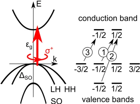
The spin-orbit coupling is the interaction of a particle with non-zero spin (here of an electron), when it is moving in an electric field, in particular in the electric field of the atoms of the crystal lattice. The effect of this interaction on the band structure of GaAs consists in and splitting of valence band into quadruplet of heavy and light holes, and double degenerate split-off band (left part of fig. 2.2). As a result, the valence states are no more pure spin states and optical transition selection rules on orbital variables will produce excitation of photoelectrons with preferential spin orientation.
Figure 2.1: Zinc blende crystal lattice (left), band structure of GaAs [Rohlfing1993] (right)
2.1.2
Initial polarization in an OP experiment
In the process of interband optical absorption of a photon with energy ℎ� > �� in the
semi-conductor, an electron in the conduction band and a hole in the valence band are generated. The symmetry of states at � = 0 together with the use of corresponding Clebsh-Gordon coefficients allows to calculate the transition probabilities induced by circularly polarized
light (fig. 2.2) [Garwin1974]. When the excitation energy ℎ� ∈ [��, �� + ∆SO], only the transitions from heavy- and light-hole bands are involved, and the spin-polarized population of photoelectrons is created in the conduction band. The initial polarization of photoelectrons in this regime is obtained as
�� = 1 − 3
1 + 3 = −
1
2 (2.1)
Here the minus sign indicates that the spin polarization is opposite to the angular momentum of absorbed photons.
Figure 2.2: Left: Direct optical transition at the center of Brillouin zone of GaAs. Valence bands are denoted as: HH (heavy hole band), LH (light hole band), SO (split-off band).
Right: Transition probabilities in an atomic-like model under �+-circularly polarized light
excitation. The fractions denote the projection of total orbital angular momentum �� of
states at � = 0, the circled numbers are the transition intensities [Dyakonov2008].
When ℎ� > �� + ∆SO, the overall polarization vanishes due to the positive contribution
of electrons photoexcited from split-off band fig. 2.3. The excitation within [��, �� + ∆SO]
results in a selection of electrons with given spin polarization.
The photoexcited carriers live some time �� before recombination, which may be radiative
(i.e., accompanied by emission of photons, which constitute the luminescence signal), or non-radiative. In direct-band gap semiconductors, like GaAs, the recombination is predominantly
radiative with a rather short lifetime of the order of �� = 10−9s at 300 K [Luber2006] and
spin lifetime �� = 10−10s [Zerrouati1988]. As we can see, for GaAs the ratio
��
�� ≈ 10
−1 (2.2)
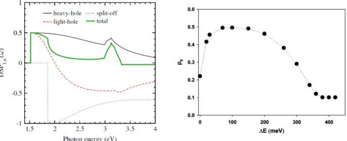
Figure 2.3: Numerically calculated dependence of the initial polarization (denoted as degree of spin polarization (DSP) in theoretical articles) on the excitation energy in GaAs, for
�− excitation [Rioux2012] (left). Same dependence, measured by two-photon spin-polarized
spectroscopy [Miah2009] (right).
The recombination of electrons with holes obeys the same selection rules as the excitation of electron-hole pairs. Therefore, the recombination of polarized electrons also produces circularly polarized light. The degree of circular polarization of the luminescence under excitation in optical pumping condition is given by:
�PL= ���el= ��2
��
�� (2.3)
where �� is the spin lifetime, �� is the conduction electron lifetime, and �el is the steady-state
electron spin polarization.
When the initial photoelectron polarization ��is known (which is the case for GaAs under
near band gap excitation), the effectively measured steady-state polarization provides impor-tant conclusions about the dynamics of spin-polarized electrons population. Using eq. (2.3) one indeed obtains the ratio of ��/��. If such experiment is combined with the measure-ment of the spin depolarization in transverse magnetic field (Hanle effect, first discovered in atoms [Hanle1924] in atoms, later in semiconductors [Parsons1969], and recently reviewed in [Dyakonov2008]), both the spin relaxation time and photoelectron lifetime can be
deter-mined. Note that, if ��can be independently measured, then the measurement of Hanle effect
allows the determination of the electron g-factor [Hermann1977].
2.2
Optical pumping in Silicon
As we just have seen in the previous section, in direct band gap III-V compounds like GaAs, all the conditions are fulfilled for an easy access to conduction electron spin physics by means of optical techniques. Indeed, the band structure (with large spin-orbit splitting and
direct band gap) plus the symmetry of the electronic states near the Γ point allows optical
orientation of photoelectron spin with a high degree of polarization (�� = −0.5) according to
the very simple scheme of fig. 2.2. Moreover, another consequence of the direct band gap is the efficient radiative recombination with a rather short electron lifetime which makes easy the determination of the electron spin polarization from the detection of the photoluminescence polarization, thus providing access to spin dynamics and intrinsic quantities like the effective electron Lande factor.
In Silicon, the situation is much less favorable mainly because of the indirect nature of the band gap. It is even surprising that optical pumping was discovered in Silicon and still determining the electron spin orientation under optical excitation remains a challenging issue both from the theoretical and from the experimental point of view.
2.2.1
Crystallographic properties of Silicon
Silicon possesses the crystallographic structure of diamond. Direct lattice is face-centered
cubic, with lattice parameter of � = 5.43 ˚A at 300 K. Its group of point symmetry is �7
ℎ, which contains, in particular the inversion symmetry. An important consequence is that the Dyakonov-Perel mechanism which plays an important role in spin relaxation in noncen-trosymmetric semiconductors, such as GaAs [Dyakonov1986], is absent in Silicon.
a
Figure 2.4: Silicon crystal lattice in real (left) and reciprocal (right) spaces
The reciprocal lattice is body-centered cubic with lattice parameter of 4��. The first
Brillouin zone (or Wigner-Seitz cell in the reciprocal space) is a truncated octahedron (the left panel in fig. 2.4). Table 2.1 recalls the position of high symmetry points of reciprocal lattice. In particular, the minimum of the lowest conduction band is achieved in six equivalent directions, also called valleys.
2.2.2
Band structure of Silicon
Silicon possesses an indirect band structure (fig. 2.5), i.e. the maximum of the highest valence band and the minimum of the lowest conduction band are located in different points
Point Position Degeneracy Axis
Γ (the center of the Brillouin zone) �0(0, 0, 0) 1
� �0(1, 0, 0) 6 ∆ � �0(12,12,12) 8 Λ � �0(3 4, 3 4, 0) 12 Σ
Table 2.1: Most important symmetry points of the reciprocal lattice. Degeneracy is the
number of equivalent directions in which these points are found. �0 = 2��
of reciprocal space. As a result, the absorption and recombination of electrons between the valence band and the conduction band are indirect (phonon-assisted) processes. An immediate consequence is that the lifetime of electrons in the conduction band is very long,
typically 10−5s.
Another particularity of Silicon is the low spin-orbit coupling. The spin-orbit splitting at
Γ is around ∆SO = 44 meV for the valence band [Nishino1974] and ∆�
SO = 30 − 40 meV for
the conduction band [Wepfer1971].
In literature the symbols Γ±
� from fig. 2.5 are often used to designate the bands only
in vicinity of the Brillouin zone (BZ) center (Γ point). However, in the present work the
symbols Γ±
� by convenience denote the corresponding bands all over the BZ.
E
ner
gyD
[eV
]
Г7-D(2x)
Г6-D(2x)
Г8+(4x)D
Г7+(2x)D
Δ
Г8-D(4x)
Δc
SimpleDgroupDnotations
DoubleDgroupDnotations
εg,X
εg,Г
εg,Г
2εg,L
directεg,L
εc
Г2-
Г4-Г5+
Г
L
X
K
Г
Figure 2.5: Silicon band structure along high symmetry directions calculated by non-local pseudopotential method [Chelikowsky1976]. Bands are labeled according to [Koster1963]. The numbers in parentheses indicate the degeneracy of bands. The energy reference is taken at the minimum of the conduction band which is located at �0(0.83, 0, 0)
The constant energy surfaces of valence bands can be described by spherical
approxima-tion only for wave vector � ≈ 0. As shown in left panel of fig. 2.6, starting from �/�0 &0.025
a strong anisotropy of constant energy surfaces (and, as consequence, of effective masses) takes place. The conduction band minimum is located away from Γ point, which implies the anisotropy of effective masses even at the minimum point itself.
For large values of wavevector �, the heavy and light holes bands are quasi-parallel along the directions � and �, with the distance between them of about 20 meV (the left panel in fig. 2.6).
Outside the center of Brillouin zone, the lowest conduction band Γ−6 bends down with a curvature which is similar to that of valence bands (the right panel in fig. 2.6). In fact, there is still few experimental evidence about the effective mass of this band. The conduction
band Γ−6 and the valence band Γ+8 are parallel over almost the entire Brillouin zone along the
direction Λ, and about the half of the Brillouin zone along the direction ∆.
All the three bands represented in fig. 2.6 are two-fold degenerate. In particular, away
from the center of zone the Γ−8 band should also split into two distinct two-fold bands.
However, the latter splitting is not reflected in the right panel of fig. 2.6 since it is not accounted for in the model proposed by Chelikowsky and Cohen.
−0.1 −0.05 0 0.05 0.1 −1.22 −1.2 −1.18 −1.16 −1.14 −1.12 k/k 0
electron energy above
ε c [eV] Γ8+ (heavy−hole band) Γ8+ (light−hole band) Γ7+ (split−off band) −0.1 −0.05 0 0.05 0.1 2.14 2.16 2.18 2.2 2.22 2.24 reduced k
electron energy above
ε c
[eV] Γ
8 −
Γ6−
Figure 2.6: Zoom near Γ point: Γ+5 valence band (left), Γ−4 conduction band (right). Negative
values of � correspond to Λ direction, positive values to ∆ direction. The bands are calculated by 30 band k.p method [Richard2004b].
Band gaps In the present work the five lowest band gaps, which are represented in ta-ble 2.2, will be of importance.
The values of the lowest optical band gaps in Silicon are measured by means of optical techniques. Spectroscopic ellipsometry allows to measure both real and complex parts of
the dielectric function �� (fig. 2.7). Its imaginary part ℑ(��) corresponds to the absorption
Name Symbol Energy Initial state Final state
Point Band Point Band
Fundamental ��,� 1.12 eV Γ Γ+5 �0(0.83, 0, 0) Γ−4 Indirect � ��,� 2.25 eV Γ Γ+5 � Γ−4 Direct � �direct �,� 3.39 eV � Γ+5 � Γ−4 First direct ��,Γ 3.35 eVa Γ Γ+ 5 Γ Γ−4 Second direct �2 �,Γ 4.17 eV Γ Γ+5 Γ Γ−2
Table 2.2: Calculated parameters of lowest band gaps in Silicon [Richard2004b]
aInstead of �
spectrum of the material. A direct optical transition is reflected in ℑ(��) by the contribution: ℑ(��) ∝ ︂ ℎ� �� ︂−2︃︂ℎ� �� ︂ − 1 Iℎ�>�g (2.4)
where ℎ� is the energy of incident photons, �� is a direct band gap (��,Γ or �2�,Γ of Silicon).
According to this equation, the transition starts to absorb once the photon energy ℎ� exceeds the gap ��. Thus, the peaks observed in the left bottom panel of the fig. 2.7 corresponds to
optical transitions. It also follows from eq. (2.4) that ℑ(��) is more sensitive to the band gap
compared to ℜ(��).
ε
g,
Г
ε
g,
Г
2
ε
g,
Г
ε
g,
Г
2
Figure 2.7: Real (top panel) and imaginary (bottom panel) parts of dielectric function of Si for different temperatures measured by ellipsometry [Jellison1983] (left). Temperature
variation of peaks on ℑ(��). The experimental data is fitted with the empirical relation of
Varshni (right).
In general, the band gap of semiconductors reduces with increasing temperature, due to the crystal expansion and interaction with phonons [Boulanger2011]. In particular, this relationship holds for the band gaps of Silicon (see table II of [Lautenschlager1987]), which constitutes the indication that the distance between conduction and valence bands increases with decreasing temperature throughout the entire BZ. The temperature variation of the
fundamental band gap of Silicon is given by [Bludau1974]:
��,�(� [K]) =
︃
1.17 + 1.059 × 10⁵� − 6.05 × 10⁻⁷�2 for 0 K < � ≤ 190 K
1.1785 − 9.025 × 10⁻⁵� − 3.05 × 10⁻⁷�2 for 150 K < � ≤ 300 K (2.5)
The right panel of fig. 2.7 represents the temperature variation of the peaks observed
on ℑ(��). The top and bottom curves provide the temperature dependence of �2
�,Γ and ��,Γ
respectively. Note that the thermal expansion of Silicon generates no additional structure.
The values for 300 K are ��,Γ= 3.28 eV and �2
�,Γ = 4.23 eV
The left panels of fig. 2.7 shows not only the change in transition energies with tempera-tures but also the increasing linewidth which in fact corresponds to the decreasing electron
lifetime ��. Indeed, �� decreases with increasing temperature because of increasing phonon
population which leads to an increase in the number of collisions between electrons and phonons.
Table 2.3 summarizes the results of different measurements of Si band gaps and valence band spin-orbit splitting. One should note that both the measurement of absorption spec-trum and photoreflectance specspec-trum are sensitive to surface induced effects due to shallow probed layer, and thus may differ from the results on bulk material. The work of [Ortega1993] is characterized by comparatively low energy resolution. So, for instance, the measured value
of fundamental gap ��,�(300 K) = 1.25 eV was significantly different from well established
��,�(300 K) = 1.12 eV. The detection of exciton and phonon structures on absorption
spec-trum allows to determine the value of spin-orbit splitting with excellent precision of 0.3 meV [Nishino1974].
One can note that the typical variation of direct gap
��,Γ(0 K) − ��,Γ(300 K) = 3.4 eV − 3.3 eV = 100 meV (2.6)
is two times higher than the variation of the indirect band gap
��,�(0 K) − ��,�(300 K) = 1.17 eV − 1.125 eV = 45 meV (2.7)
For the 115 K, which is the typical low temperature considered in the experimental part of
the present work, we take the values ��,�(115 K) = 1.162 eV and ��,Γ(115 K) = 3.382 eV. The
position of L-valley is deduced from the value of ��,Γ, applying a temperature-independent energy shift of −1.10 eV [Richard2004b].
2.2.3
Initial polarization in an OP experiment
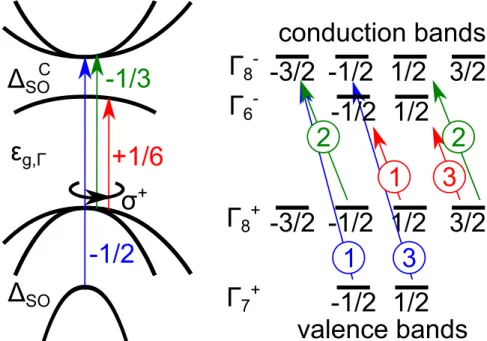
The initial electron polarization created by direct optical transition in the center of Silicon BZ can be calculated similarly to the case of GaAs. Considering the symmetry of states of Silicon, one obtains (fig. 2.8):
1 (2.8) ⎧ ⎪ ⎪ ⎪ ⎪ ⎪ ⎪ ⎪ ⎪ ⎨ ⎪ ⎪ ⎪ ⎪ ⎪ ⎪ ⎪ ⎪ ⎩ ��(Γ+8 → Γ−6) = 1(−~6) + 3( ~ 6) (~/2)(1 + 3) = 1 6 ��(Γ+8 → Γ−8) = 2(− 3~ 6) + 2( ~ 6) (~/2)(2 + 2) = − 1 3 ��(Γ+7 → Γ−8) = 1(− 3~ 6) + 3(− ~ 6) (~/2)(1 + 3) = − 1 2 (2.8a) (2.8b) (2.8c)
Temperature 1.8 − 10 K 190 K 300 K ��,Γ 3.365 eVa 3.4 eVb 3.05 eVh 3.28 eVc 3.28 eVd 3.294 eVe 3.33 eVa �direct �,� 3.45 eVb 3.36 eVd �2 �,Γ 4.18 eVa 4.185 eVf 4.135 eVf 4.1 eVh 4.23 eVc ∆SO 0.04 eVb 0.044 eVf 0.0441 eVg aelectroreflectance [Daunois1978]
bwavelength modulation spectroscopy [Zucca1970]
cellipsometry [Jellison1983]
delectroreflectance [Grover1974]
eelectroreflectance [Kondo1976]
f photoreflectance [Aspnes1972]
gabsorption spectrum [Nishino1974]
hinverse photoemission [Ortega1993]
Table 2.3: Experimental measurements of Silicon band structure parameters
The details of this calculation will be discussed further in section 6.3 of chapter 6.
However, a similar calculation of indirect optical transitions is more complex since it requires calculating the effects of electron-phonon coupling.
2.3
Proposed approach
2.3.1
Experimental: polarized photoemission
State of the art
The polarized photoemission refers to the measurement of spin polarization of electrons emitted from sample by photoelectric effect. In the case of spectroscopic measurement the kinetic energy of electrons is also analyzed. Photoemission spectroscopy allows to separate the electrons with different history in crystal. In other words, in the measured spectrum the contributions of ballistic electrons and the electrons which have undergone collisions are resolved. A characteristic feature of this method is its applicability to the study of the properties of both the electrons at the bottom of the conduction band and at the high-energy bands.
Let us concentrate on the photoemission process from bulk Silicon under optical pumping (OP) conditions. For the electron inside the crystal, one should consider three processes:
Figure 2.8: A direct optical transition at the center of Brillouin zone of Si. The
spin-orbit interaction-induced splittings of valence and conduction band are denoted as ∆SO and
∆�
SO respectively (left). Calculation of corresponding initial polarization under �+-circularly
polarized light excitation. The fractions denote �� orbital moment of states at � = 0, the
circled numbers are the transition intensities (right).
The energy dependence of the inelastic mean free path is characterized by so called ’universal’ curve, valid for metals and semiconductors (fig. 2.9). One can note that few information is available on mean free path lower than 5 eV. Furthermore, according to a classical model for low energies
� = ︂ 1 � − �F ︂2 (2.9)
mean free path diverges at � comparable with �F. For energies above 102eV the
depen-dence of the mean free path is proportional to �12.
2. The diffusion of conduction photoelectron until its recombination back to valence band.
This process is equivalently characterized by the electron lifetime �� or by its diffusion
length
�� =︀��� (2.10)
with the diffusion coefficient � given by Einstein relation � = ����
� .
3. Photoemission of conduction electrons into vacuum.
Ballistic and hot electrons experience only the processes 1 and 3, whereas for thermalized electrons the free travel between collisions appears as a part of a diffusion process on a larger time scale. Another important length scale to be considered is the depth of space charge region, which is about 10 nm.
Figure 2.9: Electron mean free path dependence on kinetic energy [Briggs1983] (left), the same curve for Silicon [Pi2000] (right)
Let us denote the spin relaxation time by �1. In fact, the discussed earlier spin lifetime
�� is defined via 1 �� = 1 �1 + 1 �� (2.11)
The eq. (6.47) can be interpreted as follows: the decay of polarization can occur either due to the spin relaxation, or due to the recombination of electrons back into the valence band. Given the eq. (6.47), the ratio of spin and electron lifetimes can be rewritten as
��
�� =
�1
�1+ �� (2.12)
Since in Silicon ��≫ �1, �� is essentially close to �1.
Two regimes of photoemission should be distinguished:
∙ In the case when the absorption length �−1 exceeds the sample thickness �: �−1 > �,
or equivalently ℎ� < ℎ�critical (regime of weak injection) [Drouhin1985]
�el = �� �1
�1+ �escape
(2.13) where
Here the escape time is of the same order of magnitude as electron lifetime. Indeed the absorption depth is long enough to suppose that creation takes place throughout the sample volume. The mean distance traveled by electrons before their escape from crystal is on the same order of magnitude as the diffusion length. Consequently the ratio of ballistic to thermalized electrons in this regime is weak. It is generally considered that the electrons thermalize quickly and then diffuse towards surface [Martinelli1970]. The diffusion of electrons is also the reason for the power 1/2-dependence of electron polarization on the ratio of lifetimes.
∙ In the case when the absorption length is lower than the sample thickness: �−1 < �, or
equivalently ℎ� > ℎ�critical (regime of strong injection), the photoemission experiment
allows to replace the lifetime by an escape time of electrons in a vacuum:
�el = ��
︃
�1
�1+ �escape (2.14)
Since the absorption coefficient is an increasing function of excitation energy ℎ�, for
fixed � this regime can also be characterized by ℎ� > ℎ�critical.
For the considered in the present work SOI samples � ≈ 10−6m, which results in ℎ�
critical ≈ 2.5 eV.
The measurement of the distributions of electron kinetic energy from Silicon was previ-ously performed by [Ebina1972; Lassailly1990; Roux2008]. The polarimetry of photoelectrons is a commonly used technique, applied to various types of samples. The polarization of elec-trons photoemitted from bulk Silicon was measured by [Bona1985; Roux2008]. Semiconduc-tor materials with lower symmetry (e.g. strained or low-dimensional structures) often yield higher spin polarization. So the polarization of 60% from Ge/GeSi/Si(1 0 0) nanostructure was recently reported [Bottegoni2011].
The inverse polarized photoemission is a similar technique for measurement the conduc-tion states. However, its applicaconduc-tion is associated with problem of low cross secconduc-tion, and as a consequence, high total charge [Yoshida2012]. Combined with angular resolution, the photoemission (direct or inverse) gives access to the electron dispersion curves along different direction.
The polarized photoemission is the most natural technique for studying the properties of hot electrons. In fact, besides the general limitation of luminescence reflected by eq. (2.3), the luminescence of hot electrons is also characterized by very weak signal level. As for magnetic resonance approach, it is also insensitive to the hot electrons.
Contribution of the present work: increasing the spin to electron lifetime ratio For semiconductors, where, like in Silicon,
��
�� ≈ 10
−3
s ≪ 1 (2.15)
a commonly used experimental approach consists in increasing this ratio via the reduction of the effective lifetime of conduction electrons. In order to increase the polarization obtained
by OP with circularly polarized light, following ways of reducing �� were considered:
∙ In the context of NMR, the enhancement of nuclear polarization by factor of 30 was
achieved with the introduction of deep recombination centers at concentration of �Au=
3 × 1016cm−3 [Bagraev1978].
∙ Roux tested similar approach with lower concentration �Au = 1014cm−3 for increasing
the initial polarization of conduction electrons detected by polarized photolumines-cence. However, no polarization above the detection limit was observed.
Methods proposed in [Verhulst2004] are related to the increase of the nuclear polariza-tion under linearly polarized irradiapolariza-tion (so called Overhauser effect), and are not directly applicable for increasing the electronic polarization under circularly polarized light excitation. In a photoemission experiment on bulk Silicon [Roux2008], the major difficulty is to
discriminate between initial polarization �� and the way it is relaxed, governed by eq. (2.15).
In fact, in such experiment a non-zero polarization is only measured in vicinity of the first direct gap. As for the excitation energy near the fundamental gap, the obtained polarization
is close to zero. Since no electron energy-resolved theoretical calculation of ��(ℎ� ≈ ��,�) is
available, it is not possible to discriminate between
∙ Low initial polarization ��(ℎ� ≈ ��,�)
∙ Presence of significant spin relaxation
In the case of the low initial polarization, it is legitimate to suppose that electrical in-jection can provide interesting results. However, the spin-LED measurements, where 30% spin-polarized electrons was electrically injected in Silicon from a ferromagnetic material, and the degree of circular polarization of the photoluminescence was measured, reveal very low polarization of nearly 3% [Jonker2007]. Similarly to spin-LED measurements, the photoe-mission is another possible approach which allows to partially lift off the limitation induced
by low initial polarization ��, since the characteristic for luminescence ��2 is replaced by ��.
The guideline to the experimental part of our work is to reduce the sample thickness in
order to replace ��by (lower) escape time, and thus to limit the ratio ��/��. In particular, the
present study is aimed is to check whether the use of thin layer of Silicon (� . ��) results in
an increase of the observed polarization under OP conditions with near ��,� light excitation.
2.3.2
Theoretical: full Brillouin zone calculation of OP
As we have seen in section 2.2.3, the analytical model of initial polarization provides only a limited description of optical pumping mechanisms in Silicon. In fact, in order to estimate the initial polarization below the direct band gap, a full Brillouin zone calculation of both the band structure and phonon dispersion relationships should be performed.
State of the art
The determination of the main band gaps (optical transition onsets) is crucial for interpret-ing optical pumpinterpret-ing experiments. But in fact, a successful complete calculation of optical pumping relies on a precise description of the band structure and electronic states all over the BZ. The ability to reproduce the experimentally measured band gaps is a prerequisite of such the description. Thus, as a preliminary step for the construction of complete OP model, it is of interest to assess the precision of different numerical methods. The fundamental concepts of density functional theory (DFT), such as local density approximation (LDA) and the GW approximation of Hedin (GW), are recalled in appendix B.
DFT A non-local pseudopotential method [Chelikowsky1976] yields the gap values in
good agreement with the experimental: ��,� = 1.17 eV, ��,à = 3.43 eV, �2
��,� = 2.15 eV, �direct
�,� = 3.37 eV. This paper is used as a reference for a number of later
experimental works.
Boulanger calculated the thermal variation of band gaps with use of Gruneisen parameters within the framework of LDA, in good agreement with experimentally observed variation.
For � = 0 K the calculation via GW yields ��,� = 1.15 eV and ��,à = 3.19 eV. Energy-only
self-consistent GW results in ��,à = 3.42 eV, whereas the full self-consistent GW overestimates
the direct gap as ��,à = 3.48 eV [Boulanger2011]. Using GW method with self-consistency
on quasiparticle part of the Green’s function, an indirect band gap of Silicon ��,� = 1.2 eV
is obtained [Shishkin2007].
The use of all-electron one-shot GW for Si, which is often considered as a reference
for pseudopotential calculations, results in ��,� = 1.19 eV, whereas the direct gaps are less
concordant with the experimental data (��,à = 3 eV, �2
�,Γ = 4.3 eV) [Ishii2010]. In this work
the � gap is given by ��,� = 2.09 eV and �direct
�,� = 3.32 eV.
[Krasovskii1999] presented an original combination of k.p and plane wave method for half space. However, the energies are much higher than the energy of the lower conduction bands of Silicon studied in the present work. The same research group described carrier injection in the regime of direct transitions within one-step photoemission model [Krasovskii2010].
Marini and Del Sole have shown that modeling excitons with Bethe-Salpeter equation results in absorption spectrum in good agreement with experimental results from [Lauten-schlager1987]. The eigenenergies for Silicon are not explicitly given [Marini2003].
k.p method The k.p method provides a quazi-analytical description of the band struc-ture based on a number of adjustable input parameters, which include in particular the eigenenergies at Γ. The result of a k.p calculation is the eigenenergies in the whole Brillouin zone. Thus, it makes sense to consider as an output of k.p calculation only the parameters
requiring the points distinct from Γ (such as ��,�, ��,�, �direct�,� ). As for parameters at ��,Γ,
�2
�,Γ, they should be directly compared with the source data for the k.p model. To date
the most precise k.p model of Silicon is the 30 band description which has been developed in [Richard2004a; Richard2004b]. The band structure parameters, calculated within this model, are given in table 2.2.
Phonon dispersion The phonons represent an integral part of optical transitions with excitation energies below the direct bang gap. In this section we present the main phonon modes in Silicon crystal. So, fig. 2.10 shows the phonon dispersion curves calculated by DFT. Since the Silicon primitive cell contains � = 2 atoms, there exists one longitudinal acoustic mode and two transverse acoustic modes, as well as 3(� − 1) = 3 optical modes.
As one can see in the fig. 2.11, the amplitude of peaks in absorption spectrum is very different for different phonon modes. For instance, the amplitude of longitudinal optical (LO) phonon peak is comparable with that of two-phonon peak implying transverse optical (TO) phonons. As will be discussed in chapter 6, the polarization of indirect optical transitions depends heavily on the phonon mode. Thus, the total polarization is in fact determined by relative intensities of phonon-assisted transitions, similar to that shown in fig. 2.11.
In Silicon, four types of phonons are distinguished, with typical energies of Γ given in table 2.4. As illustrated by third column of the table, the phonon energies can be precisely reproduced within pseudopotential numerical models.
Figure 2.10: Dispersion of phonons in Silicon. 100 cm−1 = 12.7 meV [Giannozzi1991]. Ex-perimental data are taken from [Nilsson1972]
Phonon mode Experiment [Nishino1974] Calculation [Cheng2011a]
Transverse optical (TO) 57.5 meV 57 meV
Longitudinal optical (LO) 55 meV 53 meV
Transverse acoustic (TA) 18.5 meV 19 meV
Longitudinal acoustic (LA) 46.3 meV 43 meV
Table 2.4: Energies of phonon modes at Γ
Optical pumping calculations Recent numerical calculations, which will be discussed in details in chapter 6, supply a more complete yet still partial response to the question of initial polarization. The existing numerical calculations of optical pumping in Silicon can be divided in two categories:
∙ Those considering near-indirect gap excitation [Li2010; Cheng2011a]. In these calcula-tions the initial polarization is calculated as a sum of the transition probabilities over all admissible indirect transitions.
∙ Those considering only direct optical transitions [Nastos2007].
However, all of them describe only the energy-averaged polarization, which is well suited for the comparison with the luminescence spectrum, but not with the data obtained via the polarized photoemission.
Figure 2.11: Absorption spectrum at 1.8 K with contributions of different phonon modes [Nishino1974]. The dots represent the neutron spectroscopy data from [Nilsson1972]
Contribution of the present work: energy-resolved ab initio model
In order to enable in-depth comparison with the photoemission data on OP in Silicon, an initial polarization model should include following features, none of them being present in the existing calculations:
∙ Initial polarization calculated as a function of both excitation energy ℎ� and electron kinetic energy �
∙ k-point resolution: transitions from different regions of Brillouin zone are to be calcu-lated separately
∙ Consideration of both indirect and direct optical transitions within the same compu-tational framework
The initiation of the development of such a theoretical description is the second objective of the present work.
Experimental details
3.1
Introduction
In this chapter we give an overview of the experimental setup for measuring the electron polarization under circularly polarized light excitation. We focus on the experimental tech-niques, such as the calibration of the Babinet-Soleil compensator and the Mott polarimeter. In section section 3.3 we describe the considered sample types, the photocathode preparation procedure, and characterize the photoemission yield of the studied samples.
In the following sections we present the measurable quantities, such as electron distribu-tion curve (EDC) and polarized electron distribudistribu-tion curve (PEDC), and propose original methods of their analysis. We analyze the temperature dependence of the thresholds on the EDCs, and present the interpretation of features observed in this type of spectra.
3.2
Experimental setup
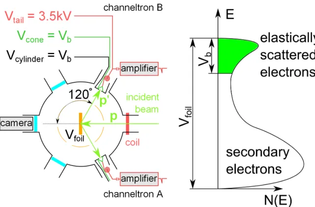
The experimental setup, which operates under ultra-high vacuum (UHV) conditions, consists of sample preparation and Mott detector chambers interconnected by the tube containing the electron spectrometer. The sample, acting as a photocathode, is mounted on a holder which allows sample heating up to 1500 K and cooling down to liquid nitrogen temperature. In the optical pumping configuration, a quartz window allows sample illumination at normal incidence. The circularly polarized light is produced by a linearly-polarized laser followed by the Babinet-Soleil compensator (the left panel of fig. 3.1). The extracted photoelectrons are energy-analyzed by the spectrometer and injected in a Mott polarimeter where their spin polarization is measured.
In order to achieve the activation of photocathodes to negative electron affinity with a
sufficient stability the working pressure should not exceed 5 × 10⁻¹⁰Torr. In particular, the
cathodes are especially sensitive to partial pressures of O2 and H2O.
Babinet-Soleil compensator sample laser spectrometer Mott polarimeter
sample holder flange
O2 leak valve pressure gauge ion pump (100 l/s) spectrometer Mott polarimeter
Figure 3.1: Setup operation principle (left), schematic view of UHV chamber (right)
3.2.1
Light excitation
Light sources
The objective of the present work is to study optical pumping in Silicon in an energy range
which starts from the fundamental band gap ��,� ≈ 1.12 eV at room temperature and extends
beyond the direct gap ��,Γ ≈ 3.3 eV. Thus we have made use of different classes of light
sources:
∙ Laser diodes:
– Infrared (IR) � = 785.2 nm, ℎ� = 1.579 eV. This light source is usually used during the cesiation procedure in order to monitor the variation of the photocurrent. – Red � = 641 nm, ℎ� = 1.934 eV
– Green � = 531.4 nm, ℎ� = 2.333 eV
∙ Kr+ laser which provide about 10 different lines from the near IR to the near ultraviolet (UV).
∙ Pulsed Ti:Sapphire laser, followed by the second harmonic generator (SHG) or the third harmonic generator (THG). Three ranges of photon energy should be distinguished:
– Fundamental range: IR light, � = 680 − 1060 nm, ℎ� = 1.17 − 1.82 eV – SHG range: visible - near-UV light, � = 340 − 530 nm, ℎ� = 2.34 − 3.65 eV – THG range: UV light, � = 267 − 353 nm, ℎ� = 3.54 − 5.47 eV
The choice of pulsed rather than continuous Ti:Sapphire laser was guided by the re-quirement to cover not only IR but also UV part of the spectrum, which is achievable with SHG/THG provided that pulsed radiation is used.
The Ti:Sapphire laser is used either in continuous or in low-power pulsed modes. Because this laser has been designed for use in pulsed mode, the operation resulted in a continuous mode power fluctuations in the long-term (more than a day) measurements, probably induced by temperature variations. A drift in wavelength of the order of the few nm was observed for some acquisitions lasting more than several days.
It should be noted that even at the optimum tuning of the pulsed mode, the radiation output always contains a continuous component. For a good tuning of the laser employed in the present work,
�continuous
�pulsed ≈ 10
−4− 10−6 (3.1)
however, this ratio may be substantially higher for the pseudo-pulsed modes.
The laser is designed for pulse generation mode TEM00, which is localized in the spot cen-ter. Continuous radiation components usually correspond to higher modes. Thus continuous components may have an uneven distribution in the plane traverse to the beam propagation direction. The latter fact was confirmed experimentally. If the (e�, e�, e�) is a Cartesian
coordinate system, and laser light propagates along e�, it is likely that �continuous(�,�)
�pulsed(�,�) can take
higher values on the periphery of the beam.
The Ti:Sapphire laser can generate an output beam with a power up to 3 W. According to the table 3.1, the SHG in the femtosecond regime yields up to 0.5 − 1 W of average optic power in the near UV, which corresponds to 25 kW and 25 MW of peak power respectively
in the case of 100 ps and 100 fs pulses at the rate �pulse = 80 MHz. The energy per pulse is
about 2.5 µJ for both regimes. The power is adjusted with help of a linear polarizer tilted with respect to the linear polarization direction at the exit of the laser.
Wavelength is measured using an Ocean Optics USB spectrometer, and later with Jobin-Yvon H25, with typical precision of ±1 nm.
Measurements of laser power are made using a bolometer with a bandwidth of the order
of �bolometer = 10 Hz. Thus, the measured values correspond to the pulsed radiation power
averaged over about
�pulse
�bolometer ≈ 10
7 pulses
both in the picosecond and the femtosecond regimes. Modulation of light polarization
Usually in similar experiments a Pockels cell is used to modulate the laser light polarization. However, in our case a long optical path would make the alignment process with the Pockels cell more difficult, so the use of the Babinet-Soleil compensator was preferred to generate
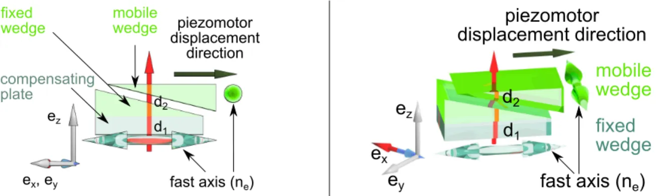
circularly polarized light. In order to change between �+ and �−, the mobile wedge of the
Babinet-Soleil compensator is mounted on a piezomotor (PI C866) with the typical precision
of 0.1 µm which corresponds to a precision of about 0.2 ˚A in the fig. 3.4. The Babinet-Soleil
compensator is rotated by 45∘ with respect to the axis of initial linear polarization of the
laser.
Picosecond Femtosecond
SHG 10% 30%
THG 3% 10%
![Figure 2.5: Silicon band structure along high symmetry directions calculated by non-local pseudopotential method [Chelikowsky1976]](https://thumb-eu.123doks.com/thumbv2/123doknet/2901212.74797/25.918.108.828.554.788/figure-silicon-structure-symmetry-directions-calculated-pseudopotential-chelikowsky.webp)
![Figure 2.11: Absorption spectrum at 1.8 K with contributions of different phonon modes [Nishino1974]](https://thumb-eu.123doks.com/thumbv2/123doknet/2901212.74797/36.918.118.795.115.554/figure-absorption-spectrum-contributions-different-phonon-modes-nishino.webp)
![Figure 3.22 shows the Cesium current and photocurrent recorded during a cesiation of SOI [5 µm].](https://thumb-eu.123doks.com/thumbv2/123doknet/2901212.74797/62.918.113.835.889.1037/figure-shows-cesium-current-photocurrent-recorded-cesiation-soi.webp)