HAL Id: tel-02305458
https://tel.archives-ouvertes.fr/tel-02305458
Submitted on 4 Oct 2019
HAL is a multi-disciplinary open access
archive for the deposit and dissemination of sci-entific research documents, whether they are
pub-L’archive ouverte pluridisciplinaire HAL, est destinée au dépôt et à la diffusion de documents scientifiques de niveau recherche, publiés ou non,
Exploration of non-volatile magnetic memory for
processor architecture
Sophiane Senni
To cite this version:
Sophiane Senni. Exploration of non-volatile magnetic memory for processor architecture. Micro and nanotechnologies/Microelectronics. Université Montpellier, 2015. English. �NNT : 2015MONTS264�. �tel-02305458�
Délivré par l’Université de Montpellier
Préparée au sein de l’école doctorale
I2S - Information, Structures, Systèmes
Et de l’unité de recherche
LIRMM - Laboratoire d’informatique, Robotique et Microélectronic de Montpellier
Spécialité: Systèmes Automatiques et Microélectroniques
Présentée par Sophiane Senni
Exploration of non-volatile
magnetic memory for processor
architecture
Soutenue le lundi 14 décembre 2015 devant le jury composé de
Jacques-Olivier KLEIN Professeur, Université Paris Sud Rapporteur Jean-Michel PORTAL Professeur, Université d’Aix Marseille Rapporteur Gregory DI PENDINA Ingénieur de Recherche, CNRS/SPINTEC Examinateur Bruno MUSSARD Ingénieur, Crocus Technology Examinateur Ian O’CONNOR Professeur, Ecole Centrale de Lyon Examinateur Abdoulaye GAMATIE Directeur de Recherche, CNRS/LIRMM Examinateur Francky CATTHOOR Directeur Scientifique, IMEC Examinateur Lionel TORRES Professeur, Université de Montpellier Directeur de Thèse
Abstract
With the downscaling of the Complementary Metal-Oxyde Semiconductor (CMOS) tech-nology, designing dense and energy-efficient system-on-chip is becoming a real chal-lenge. Reducing the CMOS transistor size faces up to manufacturing constraints leading to many issues. Regarding the energy, a significant increase of the power density and dis-sipation obstructs further improvement in performance. The increase of the leakage cur-rent leads to a significant growth of the static energy consumption in curcur-rent integrated systems. Embedded volatile memories, such as Static Random Access Memory (SRAM) and Dynamic Random Access Memory (DRAM), occupy a predominant part of the total silicon area in those systems-on-chip. As a result, a significant proportion of total power is spent into memory systems. In the past two decades, alternative memory technolo-gies have emerged with attractive characteristics to mitigate the aforementioned issues. Among these technologies, Magnetic Random Access Memory (MRAM) is a promising candidate as it combines simultaneously high density and very low static power con-sumption while its performance is competitive compared to SRAM and DRAM. More-over, MRAM is non-volatile. This capability, if present in embedded memories, has the potential to add new features to enhance energy efficiency and reliability. In this thesis, an area, performance and energy exploration of embedding the MRAM technology in the memory hierarchy of a processor architecture is investigated. A first fine-grained explo-ration was made at cache level for multi-core architectures. A second study evaluated the possibility to design a non-volatile processor integrating MRAM at register level. Fi-nally, within the context of low power applications for the internet of things, some new features brought by these emerging memory technologies were studied.
Keywords: Magnetic Random Access Memory (MRAM), non-volatility, processor, mem-ory hierarchy
Résumé
De par la réduction continuelle des dimensions du transistor CMOS, concevoir des sys-tèmes sur puce à la fois très denses et énergétiquement efficients devient un réel défi. Réduire la dimension du transistor CMOS est sujet à de fortes contraintes de fabrication, entraînant de nombreuses problématiques. Pour l’aspect énergétique, une augmenta-tion importante de la puissance dissipée par unité de surface freine l’évoluaugmenta-tion en per-formance. Ainsi l’augmentation des courants de fuite entraîne une augmentation de l’énergie statique des systèmes intégrés considérés. Notons que les mémoires embar-quées volatiles telles que la SRAM et la DRAM occupent une part prédominante de la surface silicium de ces systèmes sur puce. C’est la raison pour laquelle une partie sig-nificative de la puissance totale consommée dans les circuits actuels provient des com-posants mémoires. Ces deux dernières décennies, de nouvelles mémoires non volatiles sont apparues possédant des caractéristiques pouvant aider à résoudre ces problèmes. Parmi ces nouvelles technologies mémoires, la MRAM (mémoire magnétique) est une candidate avec un fort potentiel, elle permet d’allier une forte densité d’intégration et une consommation d’énergie statique quasi nulle, tout en montrant des performances compa-rables à la SRAM et à la DRAM. De plus, la MRAM a la capacité d’être non volatile. Ceci est particulièrement intéressant pour l’ajout de nouvelles fonctionnalités afin d’améliorer l’efficacité énergétique ainsi que la fiabilité. Ce travail de thèse a permis de mener une exploration en surface, performance et consommation énergétique de l’intégration de la MRAM au sein de la hiérarchie mémoire d’une architecture de processeur. Une pre-mière exploration fine a été réalisée au niveau mémoire cache pour des architectures multicœurs. Une seconde étude a permis d’évaluer la possibilité d’intégrer la MRAM au niveau registre pour la conception d’un processeur non volatile. Enfin, dans le cadre d’applications électroniques embarquées faible consommation pour les objets connectés, de nouvelles fonctionnalités que peuvent apporter ces technologies ont été étudiées.
Acknowledgements
First of all, I would like to thank Pr. Lionel Torres, my advisor, for his guidance, support and patience over the last three years. Thanks for giving me the opportunity to work on the fascinating field of MRAM. Thanks for the fruitful discussions we had together to complete successfully this thesis. Thanks for the invaluable advice you gave me for my future career.
Then, I would like to thank Crocus Technology which funded this thesis and thus have made this research possible. A special thank to the team I have joined at Crocus Technology, including Bruno Mussard, Alain Faburel, Christophe Gineste and Ali Alaoui for the time I spent with them during this thesis.
At LIRMM, I would also like to thank Dr. Gilles Sassatelli for his insights about the evaluation of processor architecture, Abdoulaye Gamatié for his help and advice on writ-ing papers, all the PhD students for the fruitful discussions I had with them about new research ideas, and all the people that somehow helped making the achievement of this thesis possible.
Many thanks to Pr. Ian O’Connor, Pr. Jacques-Olivier Klein, Pr. Jean-Michel Portal, Dr. Gregory Di Pendina and Pr. Francky Catthoor, who accepted to be part of my thesis committee, and for the fruitful discussions during my PhD defense.
Finally, I would like to thank a lot my family for their help and patience during the long hours I spent working on this thesis.
Contents
1 INTRODUCTION 17
1.1 Context . . . 17
1.2 Thesis objectives and contributions . . . 18
1.2.1 Objectives . . . 18
1.2.2 Contributions . . . 19
1.3 Thesis organization . . . 19
1.4 Company supporting this thesis . . . 21
2 MAGNETIC MEMORY 22 2.1 Introduction . . . 22
2.2 Basics . . . 23
2.2.1 Magnetoresistance effect . . . 23
2.2.2 Magnetic tunnel junction . . . 27
2.3 Magnetic Random Access Memory Technologies . . . 28
2.3.1 Conventional . . . 28
2.3.2 Toggle . . . 28
2.3.3 Thermally assisted switching . . . 30
2.3.4 Spin transfer torque . . . 33
2.3.5 Voltage Induced Switching . . . 34
2.3.6 Spin orbit torque . . . 35
2.4 Conclusion . . . 36
3 MRAM APPLIED TO CACHE MEMORY 39 3.1 Introduction . . . 39
3.2 State-of-the-art review . . . 41
3.2.1 3D-stacking MRAM . . . 41
3.2.2 MRAM-based non-uniform cache architecture . . . 42
3.2.3 Novel management policies for MRAM-based cache . . . 42
3.2.4 Other studies on MRAM-based cache . . . 43
CONTENTS
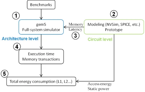
3.3 Non-volatile memory exploration flow . . . 46
3.3.1 Overview . . . 46
3.3.2 The gem5 simulator . . . 47
3.3.3 NVSim: a circuit-level model for NVM . . . 48
3.3.4 Exploration flow . . . 50
3.4 MRAM-based cache: circuit-level analysis . . . 51
3.4.1 Analysis of 512kB L2 cache . . . . 51
3.4.2 Analysis of 32kB L1 cache . . . . 53
3.4.3 Summary . . . 53
3.5 MRAM-based cache: architecture-level analysis . . . 54
3.5.1 Experimental setup . . . 54
3.5.2 Analysis of the cache memory activity . . . 56
3.5.3 Exploration of the L2 cache . . . 59
3.5.4 Exploration of the L1 cache . . . 61
3.5.5 Exploration for different number of cores . . . 63
3.6 Conclusion . . . 65
3.6.1 Area . . . 65
3.6.2 Speed . . . 66
3.6.3 Energy . . . 66
4 NON-VOLATILE MRAM-BASED EMBEDDED PROCESSOR 67 4.1 Introduction . . . 67
4.2 State-of-the-art review . . . 68
4.2.1 Non-volatile logic elements . . . 69
4.2.2 Non-volatile reconfigurable logic . . . 69
4.2.3 Non-volatile processors . . . 70
4.2.4 Summary . . . 70
4.3 Instant on/off and rollback features . . . 70
4.3.1 Amber core . . . 71
4.3.2 Instant on/off . . . 71
4.3.3 Rollback . . . 73
4.3.4 RTL simulation . . . 74
4.4 MRAM-based non-volatile processor: performance and energy . . . 78
4.4.1 Performance . . . 79
4.4.2 Energy . . . 80
4.5 Instant-on/off and sleep mode: energy analysis . . . 81
5 CONCLUSION 87
6 PERSPECTIVES 89
6.1 Further exploration at cache level . . . 89
6.2 Extension of the NVM exploration flow . . . 90
6.3 Non-volatile processor . . . 90
6.4 Security . . . 90
6.4.1 Side-channel analysis . . . 91
6.4.2 True Random number generator . . . 91
6.4.3 Physically unclonable function . . . 91
Bibliography 106
List of Figures
1.1 Memory hierarchy . . . 181.2 Thesis organization . . . 20
2.1 Magnetoresistance effect . . . 24
2.2 Giant magnetoresistance: experiment results . . . 24
2.3 Giant magnetoresistance effect . . . 25
2.4 Magnetoresistance ratio evolution . . . 27
2.5 Conventional MRAM . . . 28
2.6 Toggle MRAM . . . 29
2.7 Toggle write sequence . . . 29
2.8 MTJ structure of TAS-MRAM . . . 30
2.9 Thermally assisted switching MRAM . . . 31
2.10 Magnetic Logic Unit . . . 32
2.11 Match-in-place . . . 32
2.12 Spin transfer torque effect . . . 33
2.13 Voltage induced switching . . . 35
2.14 SOT-MRAM . . . 36
3.1 SoC area repartition between logic and memory . . . 40
3.3 Memory array organization in NVSim . . . 49
3.4 NVM exploration flow . . . 50
3.5 Quad-core architecture layout . . . 54
3.6 L2 read/write ratio . . . 56
3.7 L1 read/write ratio . . . 57
3.8 L2 cache miss rate . . . 58
3.9 L2 cache bandwidth . . . 59
3.10 L1 data cache write bandwidth . . . 59
3.11 Execution time with MRAM-based L2 cache . . . 60
3.12 MRAM-based L2 energy consumption . . . 61
3.13 Execution time with MRAM-based L1 cache . . . 62
3.14 MRAM-based L1 energy consumption . . . 63
3.15 MRAM-based L2 energy consumption for different number of cores . . . 64
3.16 MRAM-based L1 energy consumption for different number of cores . . . 65
3.17 L2 bandwidth for different number of cores (lu2 workload) . . . 65
4.1 Amber core architecture . . . 71
4.2 Amber architecture with instant-on/off computing . . . 72
4.3 MRAM-based non-volatile flip-flop architecture . . . 73
4.4 Rollback principle . . . 74
4.5 Amber architecture with instant-on/off computing and rollback capability . 75 4.6 Logic implementation of the registers . . . 76
4.7 Checkpointing and rollback . . . 76
4.8 Validation of the rollback capability . . . 77
4.9 Back-up energy . . . 81 4.10 Wake-up energy . . . 82 4.11 Energy profile . . . 82 4.12 Computing paradigms . . . 86
List of Tables
2.1 MRAM technologies . . . 383.2 512kB L2 cache features . . . . 52
3.3 32kB L1 cache features . . . 53
3.4 Architecture configuration . . . 54
3.5 Benchmarks . . . 55
3.6 L1/L2 access ratio . . . 57
4.1 Non-volatile flip-flops performance . . . 78
Acronyms
AMR Anisotropic Magnetoresistance
CAM Content-Addressable Memory
CMOS Complementary Metal-Oxyde Semiconductor
DRAM Dynamic Random Access Memory
FeRAM Ferroelectric Random Access Memory
FPGA Field-Programmable Gate Array
GMR Giant Magnetoresistance
IC Integrated Circuit
IoT Internet of Things
ISA Instruction Set Architecture
LLC Last-Level Cache
MCU Microcontroller
MeRAM Magnetoelectric Random Access Memory
MLU Magnetic Logic Unit
MR Magnetoresistance
MRAM Magnetic Random Access Memory
MTJ Magnetic Tunnel Junction
PCRAM Phase-Change Random Access Memory
RAM Random Access Memory
ReRAM Resistive Random Access Memory
SoC System-On-Chip
SRAM Static Random Access Memory
SOT Spin Orbit Torque
SOT-MRAM Spin Orbit Torque MRAM
STT Spin Transfer Torque
STT-MRAM Spin Transfer Torque MRAM
TAS Thermally Assisted Switching
TAS-MRAM Thermally Assisted Switching MRAM
1
INTRODUCTION
1.1
Context
Intensive investigations are underway to resolve the most critical problem of current nano-electronic systems: energy efficiency. Major issues encountered in today’s Integrated Circuits (ICs) include high leakage current, performance saturation, increased device variability and process complexity. For battery-powered applications, energy consump-tion is unquesconsump-tionably the most critical metric. In dynamic mode, fast switching at low power is targeted. In static mode, low leakage power is desired. Current systems embed volatile devices such as flip-flops, Static Random Access Memory (SRAM) and Dynamic Random Access Memory (DRAM), which lose information when powered off. Circuit design techniques, such as clock and power gating, are currently used to reduce the power consumed during standby mode. Although these techniques can reduce the con-sumption of static energy, it is not so easy to manage the total power concon-sumption. First, System-On-Chips (SoCs) are becoming more and more complex with the increasing num-ber of transistors per die. Regarding on-chip memories, as they are mostly volatile, sev-eral power modes are required such as active, standby, retention, deep sleep and power down for various application demands [2]. The possibility of integrating Non-Volatile Memory (NVM) would greatly facilitate the power-saving techniques implementation.
One possible way to overcome the energy efficiency issue is non-volatile SoC using non-volatile devices. In this case, a complete power down is possible with no loss of data or logic states. A promising candidate for non-volatile SoCs is magnetic memory (MRAM) based on Magnetic Tunnel Junction (MTJ) component. Both academia and industry regard MRAM as a suitable technology to become a universal memory as it combines low leakage, high density and has low access time compared to other existing and emerging NVMs such as flash, Phase-Change Random Access Memory (PCRAM) or Resistive Random Access Memory (ReRAM). However, despite the many attractive
fea-1.2. THESIS OBJECTIVES AND CONTRIBUTIONS
tures of MRAM, two challenges are still under intensive investigation. First, MTJ switch-ing requires a significant amount of current. Second, even if MTJ is orders of magnitude faster than conventional NVM, e.g. flash or embedded flash, it is slower than typical 6-transistor-based SRAM, especially for write operations. However, Toshiba recently pub-lished very encouraging results [3] on a perpendicular MTJ technology with an access time of 3ns and read/write bit energy that is almost equivalent to SRAM. MRAM has at-tracted many researchers, and many studies have been conducted to evaluate integration of MRAM in the memory hierarchy of processor architecture.
1.2
Thesis objectives and contributions
1.2.1 ObjectivesWithin the context introduced above, the global objective of this thesis is to explore how MRAM can improve the overall performance of a SoC, according to the three metrics speed/energy/area, by integrating it at different level in the memory hierarchy (Figure
1.1). This thesis focus on processor architecture.
Figure 1.1: Memory hierarchy
Although it combines attractive features such as low leakage power and non-volatility, MRAM suffers from both high write latency and energy, which need to be mitigated if integration at deep level in a SoC is desired, e.g. at register level. This thesis does not
1.3. THESIS ORGANIZATION
propose any techniques or optimizations at device, circuit or architecture level to ad-dress the drawbacks of MRAM. Instead, this work aims at setting up a fine-grain explo-ration flow to evaluate MRAM considering its current characteristics. In addition to the speed/energy/area/exploration, investigation on the potential new features that MRAM can bring into SoCs thanks to the non-volatility is also part of the objectives.
1.2.2 Contributions
As part of the contributions, this work explored use of MRAM into the memory hierarchy of processor architecture at register, cache and main memory levels. The impact in terms of performance, energy and area has been analyzed and new computing paradigms en-abled by the non-volatility of MRAM has been studied. The main contributions of this thesis are:
1. Development of a fine-grain exploration flow to evaluate NVM-based cache thanks to:
• a modified version of the gem5 simulator to model asymmetric read/write latencies
• the extraction of important information on the memory hierarchy activity: read/write ratio, dynamic/static energy ratio, miss rate, bandwidth
2. Performance/energy/area evaluation of both L1 and L2 caches based on STT-MRAM 3. Performance/energy/area evaluation of L2 cache based on TAS-MRAM
4. Validation on a full 32-bit RISC embedded processor of:
• the possibility to save/restore the complete state of a processor (instant-on/off ) • the possibility to restore a previous valid state of the processor (rollback), for
instance in the case of an execution error.
5. Analysis of a non-volatile processor with instant-on/off and rollback capabilities: • Analysis of the architectural changes
• Analysis of the impact in terms of performance and energy
1.3
Thesis organization
1.3. THESIS ORGANIZATION
Figure 1.2: Thesis organization
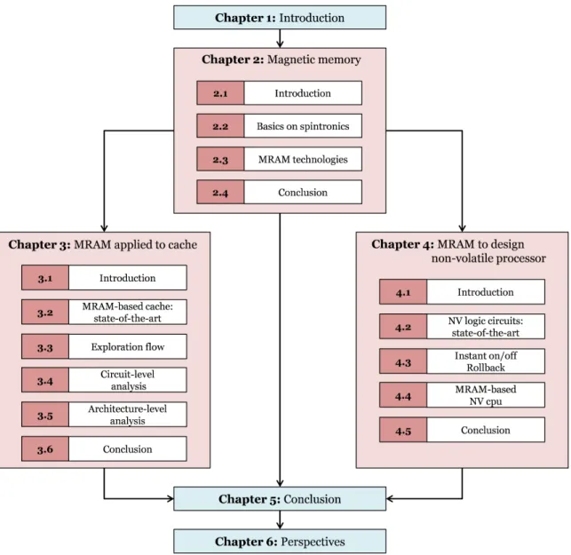
Following this introduction, Chapter2gives basics on spintronics and describes the Physics of MRAM technology. Then, existing MRAM technologies are reviewed.
Chapter4examines integration of MRAM at cache level into the memory hierarchy of multi-core architecture. First of all, previous studies on MRAM-based cache are re-viewed. Afterwards, an exploration flow to evaluate MRAM-based cache memory in terms of speed, energy, and area is described. Finally, a full exploration of MRAM-based cache at both circuit and architecture levels is reported.
Chapter4studies the possibility to have a non-volatile processor thanks to MRAM-based registers, within the context of low-power applications related to the internet of
1.4. COMPANY SUPPORTING THIS THESIS
things. Firstly, an overview of the previous works on non-volatile logic circuits is given. Secondly, this chapter introduces two features when using non-volatile registers into a processor: instant-on/off and rollback. Thirdly, performance and energy consumption of such a non-volatile processor are estimated.
Chapters5and6respectively conclude this work and give an insight on perspectives.
1.4
Company supporting this thesis
The work carried out during this thesis was funded by Crocus Technology [4], a company which develops and supplies magnetic sensors and embedded memory solutions de-signed with Magnetic Logic Unit (MLU) technology based on Thermally Assisted Switch-ing MRAM (TAS-MRAM). Due to its proprietary MLU technology, Crocus’ magnetic sensors bring significant advantages to industrial, consumer electronics and automotive applications requiring high sensitivity, high temperature, low-noise and low-cost. MLU’s distinguishing properties for enabling speed and endurance afford new levels of robust-ness to Crocus’ embedded memory solutions aimed at the Internet of Things (IoT) and security applications. Crocus is headquartered in Santa Clara, California, and has offices in Grenoble and Rousset, France. It co-owns Crocus Nano Electronics, a Russian-based advanced magnetic semiconductor manufacturing facility.
2
MAGNETIC MEMORY
2.1
Introduction
For information processing, electronics use a fundamental property of the electron: its electric charge. In the 1980s, discoveries on the spin-dependent electron transport phe-nomena gave birth to what is known today as spintronics [5]. Spintronics is a new paradigm for information storage and logic operation using another fundamental prop-erty of the electron: the spin. In this new technology, this is the electron spin that carries information instead of the electron charge. Use of spin as information is currently based on the orientation of a spin ("up" or "down") relative to a reference (e.g. magnetic ori-entation of a ferromagnetic film). The detection of the relative oriori-entation of the spin is performed using the spin-dependent electron transport properties of semiconductor-ferromagnet interfaces. Compared to semiconductor devices, spintronics-based devices are expected to be faster, more energy efficient and denser, with the capability of non-volatile data storage.
This chapter gives the basics of spin-based electronics by presenting the main discov-eries related to spin interactions with the magnetic properties of a material. In addition, an insight into the spintronic applications is given with a specific focus on memory de-vices.
The rest of the chapter is organized as follows: Section2.2 presents the major phe-nomena related to spin interactions in solid-state devices. Then, the basic element to build magnetic memories is introduced. Section2.3 reviews existing MRAM technolo-gies. Section4.6concludes this chapter.
2.2. BASICS
2.2
Basics
2.2.1 Magnetoresistance effect
In a conducting solid, the mean velocity of the electron is proportional to the electric field. This can be described as v = µ · E, where v is the mean electron velocity, µ is the electron mobility (dependent on the material), and E is the electric field. The presence of magnetic field affects the electron transport through the Lorentz force, which can be described as F = ev · B, where e is the electron charge, and B the magnetic induction. As a result, the resistance of the material varies applying a magnetic field: this is the Magnetoresistance (MR) effect. This effect (referred as anisotropic magnetoresistance) was first discovered by William Thomson in 1856. Few years later, researchers would discover two more pronounced MR effects known as the giant magnetoresistance and the tunnel magnetoresistance. The rest of this section will describe these three MR effects.
Anisotropic magnetoresistance
William Thomson discovered the Anisotropic Magnetoresistance (AMR) through exper-iments on iron and nickel. He observed a variation of the electrical resistance when an external magnetic field is applied. The electron scattering (i.e. electrons are deviated from their original trajectory) rate is affected depending on the direction of the field. When the magnetization is perpendicular to the current direction, the electron scattering is smaller, whereas when the magnetization is parallel to the current direction, the electron scatter-ing is larger. Figure2.1illustrates the AMR effect resulted by the interaction between the magnetization (green arrows in the figure) and the electron spin. Electrons whose spin is in the opposite direction of the magnetization (white spheres in the figure) are scattered more than electrons whose spin is parallel with the magnetization (red spheres in the figure). In ferromagnetic materials, AMR affects the resistance in the order of a few per-cent. However, in the late 1970s, it was sufficient to successfully develop AMR sensors to replace inductive sensors as the read head in hard-disks.
Giant magnetoresistance
In the late of 1980s, two groups of researchers, led by Albert Fert and Peter Grünberg, independently discovered the Giant Magnetoresistance (GMR) effect in structures alter-nating ferromagnetic (FM) and non-magnetic (NM) layers. The group of A. Fert investi-gated the MR of thirty to sixty stacked Fe/Cr structures and observed almost a factor of 2 between the resistivities at zero field and in the saturated state, respectively [7] (Figure
2.2. BASICS
Figure 2.1: Magnetoresistance effect [6]
structure and noticed that an anti-parallel alignment of the magnetization of the Fe layers increases the electrical resistivity, much more than AMR effect.
Figure 2.2: Giant magnetoresistance: experiment results on N stacked Fe/Cr structures with N = 30, 35 and 60 at 4.2K [7]
Grünberg and his group explained this effect by spin-flip scattering, as shown in Fig-ure2.3. When the spin of the electrons is parallel to the direction of magnetization of the FM layer, the electrons are weakly scattered and the FM layer shows a small resistance. On the other hand, when the spin of the electrons is anti-parallel to the direction of mag-netization of the FM layer, the electrons have a strong scattering and the FM layer shows a large resistance.
With no external magnetic field, the FM/NM/FM structure shows an anti-ferromagnetic behavior (i.e. the magnetization of the FM layers are in opposite direction). In such
struc-2.2. BASICS
Figure 2.3: Giant magnetoresistance effect [6]
ture, both the spin-up electrons and the spin-down electrons will have a strong scatter-ing since they will necessary cross a layer with a magnetization anti-parallel to the spin. When an external magnetic field is applied, both FM layers are aligned in the same di-rection. As a result, the electrons whose the spin is parallel to magnetization of the FM layers will be weakly scattered. In this case, the electrical resistivity is lowered compared to the anti-parallel configuration of the structure.
The material has a resistance consisting of two resistances in parallel. One resistance for the spin-up electrons and on resistance for the spin-down electrons. If we consider
R↓ as the resistance of a FM layer with weak scattering, and R↑ as the resistance of a
FM layer with strong scattering, then the total resistance of the parallel (anti-parallel) configuration of the structure can be given by the equation2.1(equation2.2):
Rp= (2 · R↓) k (2 · R↑) = 2 · R↑· R↓ R↑+ R↓ (2.1) Rap= (R↑+ R↓) k (R↓+ R↑) = R↑+ R↓ 2 (2.2)
Therefore, the difference in resistance between the two configurations is given by the equation2.3:
2.2. BASICS ∆R = Rp− Rap = −1 2 (R↑− R↓)2 R↑+ R↓ (2.3) Tunneling magnetoresistance
Tunneling Magnetoresistance (TMR) is a phenomenon first discovered by Tedrow and Meservey in 1970 [8]. They observed that the tunneling electrons through junctions be-tween very thin superconducting aluminum layers and ferromagnetic nickel layers is spin dependent. In 1975, Michel Jullière studied the conductance of two ferromagnetic layers separated by a thin insulator [9]. He measured the tunneling conductance depen-dence on voltage at 4.2K. He observed on a Fe/Ge-O/Co structure a relative resistance change of 14% at zero bias, and 2% when the voltage bias is increased at 6mV.
Unlike GMR which is related to electron scattering, TMR relies on the spin polar-izations of the conduction electrons. In a parallel configuration of the material, elec-trons whose spin is parallel to the direction of the magnetization of the layers will tunnel through the barrier, whereas electrons whose is parallel will be filtered. In an anti-parallel configuration of the structure, both spin-up and spin-down electron flows are reduced, resulting in a large resistance.
Jullière measured the conductance ratio, which is known today as the TMR ratio given by the equation2.4, where P1and P2 are the spin polarizations of the two ferromagnetic
layers: T M R = ∆R Rp = Rap− Rp Rp = 2 · P1· P2 1 − P1· P2 (2.4)
In 1995, Terunobu Miyazaki and Nobuki Tezuka reported a TMR ratio of 2.7% at room temperature in a NiFe/Al2O3/Co structure [10]. In the same year, Moodera et
al. observed the first giant TMR ratio of 11.8% in a Al2O3-based junction at room
tem-perature [11]. Since 2004, junctions based on a Al2O3 barrier have reached a TMR ratio
of 70% [12]. However, the breakthrough regarding the TMR ratio will come with bar-riers based on the MgO. In 2001, Butler et al. and Mathon and Umersk theoretically predicted that a giant TMR ratio higher than 1000% could be obtained in fully epitaxial
2.2. BASICS
Fe(001)/MgO(001)/Fe(001) structure [13,14]. In 2008, experimental TMR reached 600% at room temperature in a CoFeB/MgO/CoFeB junction [15].
The TMR effect have raised a great interest to design spintronic devices. Figure2.4
summarizes the evolution of the magnetoresistance ratio and the device applications. The following section will describe the magnetic tunnel junction as a data storage unit.
Figure 2.4: Magnetoresistance ratio evolution [16]
2.2.2 Magnetic tunnel junction
A MRAM bit is a MTJ consisting of two ferromagnetic layers separated by a thin insulat-ing barrier. The information is stored as the magnetic orientation of one of the two layers, called the free layer (FL) or storage layer. The other layer, called the reference layer or fixed layer (RF), provides the fixed reference magnetic orientation required for reading and writing. The TMR effect causes MTJ resistance to depend significantly on the relative orientation of the two magnetic layers: the antiparallel state provides much larger resis-tance than the parallel state. It enables the magnetic state of the FL to be sensed thanks to a current flowing through the MTJ. Hence, stored information can be read. Five methods have been proposed to switch the orientation of the FL: toggle [17], Thermally Assisted Switching (TAS) [18], Spin Transfer Torque (STT) [19], voltage-induced switching and the most recent method is called Spin Orbit Torque (SOT) [20].
2.3. MAGNETIC RANDOM ACCESS MEMORY TECHNOLOGIES
2.3
Magnetic Random Access Memory Technologies
2.3.1 Conventional
A conventional MRAM, shown in Figure 2.5, uses a simple way to program the MTJ where sufficient magnetic field is generated thanks to a combination of two current flows applied simultaneously through a row and a column of an MTJ array. Two problems arose with this method. First, large current is needed to generate sufficient magnetic field to reverse the magnetization of the FL. Second, this approach suffers from selectivity problem: some of the bits sharing the same row or column of the cell being programmed might be exposed to sufficient magnetic field and be switched unintentionally. This effect is one consequence of process variability. The magnetic field necessary to reverse the magnetization is not exactly the same for all the bits [21].
Figure 2.5: Conventional MRAM [22]
2.3.2 Toggle
This technology is currently commercialized by Everspin [23]. Figure 2.6 illustrates a standard toggle MRAM MTJ. A Complementary Metal-Oxyde Semiconductor (CMOS) access transistor provides a current through the MTJ needed for the read operation. Each MTJ is located at the intersection of two conductive lines, IWORDand IBITin Figure 2.6.
Toggle MRAM was proposed to deal with the selectivity problem observed in the stan-dard MRAM. The toggle MRAM adds a second FL and an anti-ferromagnetic coupling layer above the first FL, as shown in Figure2.6. In addition, a specific timing sequence of the write-current pulses, shown in Figure2.7, is used to switch only the MTJ at the inter-section of the conductive lines. These changes improve the stability of the magnetic ori-entation of the bit cell and avoid the selectivity issue. Unlike other MRAM technologies,
2.3. MAGNETIC RANDOM ACCESS MEMORY TECHNOLOGIES
the toggle MRAM scheme does not drive the bit cell to a predetermined state, instead it always reverses the current magnetization of the FL. As a result, a read of the current state of the MTJ is required before a write if the opposite state is desired.
Figure 2.6: Toggle MRAM [22]
The toggle MRAM has certain limitations. Although it resolves the selectivity issue of the conventional MRAM, it still needs a significant amount of current to switch the bit cell, thereby limiting the upper bound of the write speed. Moreover, the amount of current needed for writing remains almost the same even when the size of the bit cell is reduced. Consequently, the selectivity issue can appear again when scaling the MTJ. In addition, as the switching current does not shrink scaling the technology node, the area of the peripheral circuits of the MTJ array also remains the same, thus limiting the density [21]. Toggle MRAM is not predicted to be suitable at nodes less than 90 nm.
2.3. MAGNETIC RANDOM ACCESS MEMORY TECHNOLOGIES
2.3.3 Thermally assisted switching
The aim of the TAS concept was to improve the downsize scalability of MRAM. The concept was developed by the SPINTEC laboratory and TAS-MRAM is currenly com-mercialized Crocus Technology. As shown in Figure2.8, TAS-based MTJ uses an anti-ferromagnetic layer (low TBin Figure2.8) to block the magnetic orientation of the FL
un-der a threshold temperature. To switch the bit cell, a select transistor provides a flow of current to heat the MTJ above the blocking temperature thereby enabling storage of new information thanks to application of a magnetic field. Heating the FL allows TAS-MRAM to use a smaller magnetic field and hence less current than toggle MRAM to write the bit cell, since a single conductive line is sufficient to generate the required magnetic field. Blocking the FL’s state using a coupling anti-ferromagnetic layer also significantly im-proves data stability, even scaling the technology node. As a result, TAS-MRAM makes it possible to reduce the switching energy while ensuring excellent data retention. This new method also solves the selectivity issue, since the MTJ has to be heated before writing.
Figure 2.8: MTJ structure of TAS-MRAM [18]
Figure2.9shows a complete TAS write operation. Assuming the MTJ stores a “0” state (parallel state), the first step in the TAS method is to heat the FL by flowing a current through the MTJ to reach the blocking temperature (heating step in Figure 2.9). The second step is to generate an external magnetic field to switch the FL while heating the MTJ (switching step in Figure 2.9). Once the FL switches to the “1” state, the CMOS transistor responsible for the heating process is switched off whereas the MTJ remains under the external magnetic field (cooling step in Figure2.9).
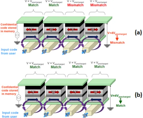
Crocus technology designed another implementation of TAS-based MTJs, called MLU [25], in which the reference layer (RL) is replaced by a self-reference layer (SRL). As a re-sult, the SRL can easily be switched by applying an external magnetic field because the magnetic orientation of the SRL is not fixed like that of the RL, as shown in Figure2.10.b. While the write scheme remains the same, the read operation is quite different. In this
2.3. MAGNETIC RANDOM ACCESS MEMORY TECHNOLOGIES
Figure 2.9: Thermally assisted switching MRAM [24]
case, reading consists of two steps: the MTJ resistance is measured while the magnetiza-tion of the SRL is set in one direcmagnetiza-tion. The MTJ resistance is then measured again when the magnetization of the SRL is reversed to the opposite direction. The resistance varia-tion between the two measurements provides informavaria-tion about the magnetizavaria-tion of the FL. The new approach increases the read time, but tolerance to process variation is clearly improved since each bit cell is self-referenced. Moreover, this approach significantly re-duces reading errors. Usually, the two resistance states need to be well separated, which can lead to manufacturing problems when scaling the technology node. For MLU, using the difference in the two states for reading is not sensitive to this manufacturing problem. The innovative MLU concept also leads to another interesting feature: the device can also act as an exclusive-OR logic gate (XOR). Assuming that the two magnetic layers are the inputs and the MTJ’s resistance is the output, the truth table of a XOR logic gate can be built (Figure 2.10.c). This makes MLU a particularly useful component of security applications. An example of application introduced by Crocus technology is the match-in-place [25], shown in Figure2.11. If the current direction applied on the field line during a read operation is considered as an information input, the device can use its XOR logic capability to compare in situ the data stored in memory with the input and control if there is a match or a mismatch comparing the output resistance with a reference. Other possible applications of MLU are: content-addressable memory, NOR-MRAM, NAND-MRAM [24].
Although the structure of TAS-MRAM means it has better scalability than toggle MRAM, TAS-MRAM needs a non-negligible time to complete its write operation due to the heating/cooling processes. Moreover, since an external magnetic field is used to switch the MTJ, the amount of current is still high, even if it is lower than for the toggle. One possible way to reduce the switching energy is to combine the TAS method with the STT effect. TAS-MRAM is expected to be scalable down to 45 nm [24]. However, the aim
2.3. MAGNETIC RANDOM ACCESS MEMORY TECHNOLOGIES
Figure 2.10: Magnetic Logic Unit: (a) Magnetic stack of TAS-MRAM (b) Magnetic stack of MLU (c) Virtual XOR logic gate of MLU [24]
2.3. MAGNETIC RANDOM ACCESS MEMORY TECHNOLOGIES
of TAS-MRAM is its high thermal stability thanks to its MTJ structure. The latter allows very good data retention, and good reliability against magnetic field disturbance [24].
2.3.4 Spin transfer torque
Spin Transfer Torque MRAM (STT-MRAM) appeared with the need to reduce the switch-ing energy consumption of MRAM. Unlike the previous MRAM technologies, which use an external magnetic field to program a bit cell, STT-MRAM write operations are based on another physical phenomenon to switch the magnetic orientation of the FL called STT. The idea is that the FL can be switched by direct transfer of the spin angular momen-tum from spin-polarized electrons. In this way, a highly spin-polarized current flowing through the MTJ causes a “torque” applied by the injected electron spins on the magneti-zation of the FL. Applying sufficient current will cause sufficient torque to switch the bit cell, thereby enabling information to be written. Figure2.12depicts the STT effect.
Figure 2.12: Spin transfer torque effect: (a) illustration of the transition from an antipar-allel to a parantipar-allel state, and (b) the transition from a parantipar-allel to an antiparantipar-allel state [19]
Figure2.12.a shows the transition from an antiparallel to a parallel state. In this case, electrons go through the fixed layer first, and the fixed layer acts as a polarizer. Thus, electrons are spin-polarized in the magnetic orientation of the fixed layer. Once the insu-lating barrier (MgO) is crossed, the spin-polarized electrons exert torque on the magneti-zation of the FL until a magnetic orientation reversal occurs. A similar effect is depicted in Figure2.12.b for the transition from a parallel to an antiparallel state. In this case, elec-trons go through the FL first. While the majority of the elecelec-trons will be spin-polarized in the magnetic orientation of the FL, a minority of electrons will still be spin-polarized in the opposite direction of the FL. These minority electrons will be reflected at the barrier interface and will exert torque on the magnetization of the FL.
2.3. MAGNETIC RANDOM ACCESS MEMORY TECHNOLOGIES
plane and perpendicular. In-plane magnetization is also used in toggle MRAM and TAS-MRAM, in which the magnetic orientation is parallel to the plan of the MTJ, whereas in perpendicular magnetization, the magnetic orientation is perpendicular to the plan of the MTJ. Perpendicular STT-MRAM was introduced to further reduce the switching cur-rent of the MTJ and to improve scalability.
State-of-the-art showed that STT-MRAM read access time is similar and sometimes better than its SRAM equivalent [26, 27, 28]. Concerning write operations, despite the fact that STT-MRAM considerably reduces switching energy compared to the previous MRAM technologies, some limitations were observed. Some of them were mitigated or eliminated while others still remain.
First, read and write operations use the same path, which can lead to unexpected writes when reading is underway, particularly with advanced technology nodes. To mit-igate this issue, a solution was proposed at device level designing a three-terminal dual-pillar MTJ structure with two spatially and electrically independent ports for writes and reads [29].
Second, the current needed to switch the MTJ from the parallel to the antiparallel state (and vice-versa) is not symmetrical [30]. Switching from a parallel to an antiparallel state requires more current than the reverse. This is because switching from an antiparallel to a parallel state is performed by spin-polarized electrons going through the MTJ (majority of the electrons), whereas switching from a parallel to an antiparallel state is performed by reflected spin-polarized electrons (a minority of the electrons). A solution was also proposed to eliminate this problem by adding a complementary polarizer [31,32]. In this proposed device, the MTJ has two pinned layers instead of one, with opposite magnetic orientations. Depending on the information to write, the switching current will flows through the corresponding pinned layer.
Third, STT-MRAM is confronted to scalability issue. When a STT-MRAM cell is scaled, the thermal stability factor scales down linearly with the area, and can cause unreliability due to retention failure [33]. Moreover, although its switching energy re-mains low compared to Toggle and TAS-MRAM, STT-MRAM needs access transistor sizes larger than the minimum size at advanced node (32 nm and below) [34], limiting thus the memory density . This is an issue also for high performance applications which require high write speed, since the switching current of STT-MRAM increases when the write pulse width decreases.
2.3.5 Voltage Induced Switching
In order to improve the scalability and reduce the switching energy observed with STT-MRAM, a voltage-controlled MTJ were proposed [35,36,37,38,39], also known as Magnetoelectric
2.3. MAGNETIC RANDOM ACCESS MEMORY TECHNOLOGIES
Random Access Memory (MeRAM). As shown in Figure2.13, this approach uses voltage rather than current to reverse the magnetization of the free layer thanks to the recently demonstrated voltage-controlled magnetic anisotropy effect (VCMA) [40]. The free layer has a magnetic anisotropy that can be changed by voltage. Hence, voltage-induced switching of the magnetization can be performed modifying the magnetic anisotropy of the MTJ. The voltage-controlled MTJ (VMTJ) structure uses materials commonly used by previous MRAM technologies, thus maintaining manufacturability [35]. VMTJ has an unipolar voltage-controlled behavior, i.e. switching is performed by set/reset voltages of different amplitudes but same polarity, whereas STT-MRAM uses opposite current polarities to switch the bit cell.
Figure 2.13: Voltage induced switching [35]
Since switching for VMTJ is performed via voltage, the barrier thickness can be in-creased to reduce the parasitic conductance and hence the effect of current-induced torques (i.e. STT effect). Moreover, a high TMR (greater than 100%) is possible allowing the read-out of the magnetization of the free layer [41]. Although it is still at experimental level and needs further improvements in the design, MeRAM is expected to improve the scal-ability by eliminating the need for large currents, which is currently a real issue with STT-MRAM for advanced technology nodes.
2.3.6 Spin orbit torque
Spin Orbit Torque MRAM (SOT-MRAM) is the most recent technology for MRAM. It was developed to mitigate the issues observed in STT-MRAM. Contrary to STT-MRAM, this new technique uses a three-terminal structure to separate the read and write paths, as shown in Figure2.14.b. The physical effect responsible for the reversal of magnetization
2.4. CONCLUSION
or the spin Hall effect [43] could explain the switch in magnetization of the storage layer.
Figure 2.14: SOT-MRAM: (a) Conventional STT-MRAM (b) SOT-MRAM [44] Unlike STT-MRAM, SOT-MRAM intrinsically separates the read and write paths and allows symmetrical switching current between the two states of the MTJ. Hence, read stability is improved, strongly reducing the possibility of a bit flip (the bit changes its state) during a read operation. Also, designers can optimize the read and write sepa-rately. On the other hand, SOT-MRAM has a bigger cell size than STT-MRAM because of its three-terminal structure. As SOT-MRAM is a young technology compared to other MRAM technologies, further research is needed to optimize the SOT-based MTJs. Like MeRAM, a great potential is expected from this technology to reach same performance as SRAM.
2.4
Conclusion
This chapter presented the main phenomena related to the MR effect, which lead to the development of MRAM technology. As described above, a material consisting of alter-nate FM and NM layers shows lowest electrical resistance when the magnetic moments of the FM layers are aligned, and highest electrical resistance when they are anti-aligned. Thus, it was observed that the transport of the electrons is spdependent due to in-teractions between the electron spin and the magnetic properties of the material. This discovery marked the beginning of spintronics. Advances on the MR effect allowed to reach a ratio of more than 100% between the lowest and the highest resistance of a
mate-2.4. CONCLUSION
rial. As a result, MRAM technologies emerged and intensive investigations are currently underway to improve their performances. To have an overview of the differences be-tween them, MRAM technologies reported above are summarized in Table2.1. Due to its voltage-controlled switching scheme, MeRAM needs a very low write current compared to other MRAM technologies. Hence, very high scalability is expected. STT-MRAM and SOT-MRAM show almost the same overall performance and are very good candi-dates to be part of the memory hierarchy of SoCs. Unlike SOT-MRAM, first test chips have already been developed for STT-MRAM. Compared to other MRAM technologies, TAS-MRAM is the most reliable thanks to its MTJ structure which allows excellent ther-mal stability, and then very good data retention.
The following chapters analyze integration of some MRAM technologies into the memory hierarchy of processor architecture. Chapter4focus on multicore architecture and evaluate MRAM in cache memory. Chapter4explore the benefits of having a non-volatile processor including MRAM at register level.
Compared to other MRAM technologies, Toggle MRAM has a very high switching energy and and its scalability is limited. Hence, it is not considered for the remaining of this report. Although MeRAM and SOT-MRAM show very promising performance, they are always at experimental level and need further development. On the contrary, TAS-MRAM and STT-MRAM are quite mature since test chips already exist [45,46,47,4]. Therefore, only these two technologies are considered for the next chapters.
2.4.
CONCLUSION
Technology Cell size (F2) Access time Write current Endurance Maturity Advantages/Drawbacks
read/write
Toggle MRAM 50 35 ns / 35 ns >30 mA 1015 Commercialized (+) Maturity (-) High power [17, 22,23]
TAS-MRAM <50 30 ns / 30 ns A few mA 1015 Test chip (+) Reliability
(-) Access time
[4,18,24] [4]
STT-MRAM <50 2-20 ns / 2-20 ns 50 uA > 1016 Test chip (+) Low power
(-) Reliability
[19, 30] [45,46,47]
MeRAM <10 <10 ns very low > 1016 Prototype (+) Low power (-) Maturity [41, 48]
SOT-MRAM <50 A few ns <100 uA > 1016 Prototype (+) Low power
(-) Maturity [26, 44,49]
3
MRAM APPLIED TO CACHE MEMORY
3.1
Introduction
Since the advent of ICs, the number of transistor per die never stops increasing to reach today several billion of transistors [50]. The decreasing size of the CMOS transistor has made possible the fabrication of small devices able to run at high speed. On the other hand, the power consumption of SoC has significantly increased due to the high density of integrated components. As a result, current nanoelectronic systems are confronted with heat issue because of the high power dissipation, which is a real obstacle to the increase of the frequency. With the limit of the frequency scaling, a shift to parallel com-puting has been observed to form the era of multi-core processors.
Regarding the three metrics speed/energy/area, memory is a key element for future SoCs. Richard Sites, one of the fathers of computer architecture, said in his article entitled "It’s the memory, Stupid!" [51]:
Across the industry, today’s chips are largely able to execute code faster than we can feed them with instructions and data. . . The real design action is in memory subsystems—caches, buses, bandwidth, and latency.
Since processing elements have to be fed with instructions and data from memories, the latter plays an important role on the overall performance of the system. Furthermore, an increasing trend of embedding more volatile memory in SoCs is observed. As shown in Figure3.1, memory systems occupy more than half of the die area. As a consequence, a significant proportion of total power is spent on memory systems (Figure 3.2). The predominant technology is SRAM, currently used for both cache memory and registers because of its fast access time compared to other technologies. However, it consumes more and more static energy due to the increase of the leakage current when decreasing
3.1. INTRODUCTION
Figure 3.1: SoC area repartition between logic and memory (from Semico Research Cor-poration [52])
Figure 3.2: SoC energy repartition between logic and memory (from ITRS [53])
In the past two decades, alternative memory technologies have emerged with attrac-tive characteristics to mitigate the aforementioned issues. Among these technologies, MRAM is a promising candidate as it combines simultaneously high density and very low static power consumption while its performance is competitive compared to SRAM and DRAM.
This chapter presents a fine-grain exploration to evaluate the performance and energy impacts of including MRAM in the memory hierarchy of processor architecture. The
ex-3.2. STATE-OF-THE-ART REVIEW
ploration is discussed based on L1 and L2 cache memories. In the present study, useful information about the memory traffic are extracted, such as the cache miss rate and the cache bandwidth. This information is monitored over time to better understand the be-havior of the workloads in terms of memory access. Hence, a clear vision of the influence of these parameters on performance and energy is possible. In addition, a set of data including the read/write ratio, the static/dynamic energy ratio and L1/L2 access ratio are also extracted to better analyze the impact of the different read/write latencies, of the high dynamic energy and of the low leakage of MRAM, thus enabling fine-grain analysis of the performance and the total energy consumption of MRAM-based cache.
The rest of the chapter is organized as follows: Section4.2reviews the state-of-the-art on MRAM-based cache memory. Section3.3describes the NVM exploration flow used in this study to allow a fine-grain evaluation of including MRAM in the memory hierarchy of processor architecture. Section3.4 analyzes and compares both MRAM and SRAM caches at circuit level. Section3.5explores MRAM-based cache at architecture level for both L1 and L2 caches (L2 as last-level-cache). Section4.6concludes this chapter.
3.2
State-of-the-art review
Many studies have been conducted on integration of MRAM into the memory hierarchy of single-core and multi-core architectures. All these studies explored a hybrid cache hierarchy using SRAM and STT-MRAM technologies, but a few studies also explored use of DRAM and PCRAM. Most of the studies evaluated the use of STT-MRAM for last-level cache (Last-Level Cache (LLC)). A few authors explored MRAM for upper last-levels of cache such as L1.
3.2.1 3D-stacking MRAM
Some authors studied the benefit of the 3D-stacking ability of MRAM combined with its high density to evaluate 3D-processor architecture. They analyzed the performance and energy impacts of having a MRAM-based LLC on top of a 2D-processor architecture. [54] and [55] evaluated a 3D-stacked STT-MRAM-based L2 on top of a 2D-processor architec-ture. Considering the same area constraint, use of MRAM in L2 results on a 89% and 73%total power reduction compared to a conventional L2 based on SRAM. [56] explored three different memory hierarchy configurations with hybrid L2/L3 cache architectures using MRAM, PCRAM and embedded DRAM in an 8-core processor considering a 3D chip integration. Under the same area constraint and considering a 3-level cache hierar-chy in which L1 is based on SRAM, results showed 18% IPC1 improvement and up to
3.2. STATE-OF-THE-ART REVIEW
70%of total power reduction over a 3-level cache hierarchy based on SRAM only.
3.2.2 MRAM-based non-uniform cache architecture
Other authors explored non-uniform cache architectures (NUCA) using both SRAM and MRAM in one cache level. [57] and [56] proposed a hybrid cache consisting of a large but slow MRAM-based region and small but fast SRAM-based region. Using data migration policies, the objective is to write mostly in the SRAM region (because it is faster) and to read data from the MRAM region. In this way, performance degradation due to the high write latency of MRAM can be mitigated. In addition, larger cache capacity is possible thanks to the high density of MRAM. Simulation results of such a hybrid cache in L2 showed 55% of the total power reduction on average and 5% IPC improvement over a SRAM L2 baseline. [58] proposed a hybrid SRAM/STT-MRAM cache architecture for chip-multiprocessors. In addition, micro-architectural mechanisms were introduced to reduce the number of writes in STT-MRAM regions. Considering an 8-core architecture, use of this hybrid SRAM/STT-MRAM architecture in a shared L2 cache showed that the overall power consumption is reduced by 37.1% and performance is improved by 23.6%on average compared with SRAM based static NUCA L2 cache under the same area configuration.
3.2.3 Novel management policies for MRAM-based cache
Several cache management techniques have been proposed to mitigate the two main drawbacks of MRAM (high write latency and high write energy). [59] proposed a novel technique called early write termination (EWT). EWT aims at removing unnecessary writes (i.e. writing same value) to reduce the write energy consumption in the cache. Because MTJ does not switch gradually but abruptly at the end of a STT-based write, this technique proposed to read the stored value during a write operation and to stop the write if it is redundant. Considering a 4-core architecture, evaluation of the EWT tech-nique on a shared L2 cache based on STT-MRAM shows that up to 80% of write energy reduction can be achieved through EWT, resulting on 33% less total energy consump-tion, and 34% reduction in energy-delay product compared to a STT-MRAM-based L2 cache without EWT. [55] introduces the read-preemptive write buffer technique in which write buffers are used to mitigate the long write latency of MRAM. In addition, when there is a conflict between a read (from the upper level cache) and a write (from the write buffer), a read-preemptive policy gives priority to the read in order to prevent write op-erations from blocking read opop-erations due to the long write latency of writes. By using the read-preemptive write buffer technique on a STT-MRAM-based L2, results showed up to 9% of performance improvement and up to 67% of power reduction compared to
3.2. STATE-OF-THE-ART REVIEW
SRAM-based L2. [28] proposed a similar technique called the obstruction-aware policy (OAP) for cache management of a single-port STT-MRAM-based L3 (LLC). In addition to preventing the delay of several read operations caused by a long write operation, OAP can mitigate the performance degradation of the MRAM-based LLC while significantly reducing total energy consumption thanks to the ultra-low leakage of MRAM. After adopting OAP and considering 4-core system with an 8MB STT-RAM L3 cache, results showed 14% performance improvement on average, and a reduction of 64% on the to-tal L3 energy consumption. [60] proposed a new STT-MRAM cache architecture called asymmetric write architecture with redundant blocks (AWARE) to reduce the average cache write latency. This is done by taking advantage of the asymmetric write character-istics of STT-MRAM. Use of this technique on a STT-MRAM-based L2 cache showed a reduction of the average cache write latency by 30% over conventional STT-MRAM cache design, at the cost of an increase of the cache write energy by 7%.
3.2.4 Other studies on MRAM-based cache
Among studies on MRAM-based cache, [61] evaluated the performance/energy impacts of a STT-MRAM-based L2 when the retention time of the MTJ is reduced. Reducing the retention time of the MTJ can reduce both switching energy and switching latency. 10+ years, 1s and 10ms retention times for STT-MRAM were explored. In addition, a cache re-vive policy was proposed for the 10ms-retention-time-based STT-MRAM to refresh data if necessary. Using this scheme on a L2 cache based on STT-MRAM showed an aver-age 10 − 12% improvement in performance compared to the traditional SRAM-based L2 cache design, while reducing the energy consumption by 60%. [62] proposed fine-grain power gating on STT-MRAM peripheral circuits to further reduce the total energy con-sumption of STT-MRAM-based LLC. The simlation results showed a reduction up to 80% of leakage power in state-of-the-art STT-MRAM LLC. [26, 44] made a first study of using the new SOT-MRAM technology in caches. Both SOT-MRAM-based L1 and L2 were explored and compared with SRAM-based and STT-MRAM-based caches. The best configuration simulated was a hybrid combination of SRAM for the L1-Data-cache, SOT-MRAM for the L1-Instruction-cache and L2-cache, which can reduce the energy con-sumption by 60% while the performance increases by 1% compared to an SRAM-only configuration. Although this work is close to the study presented in this chapter, some important aspects on the architecture and the memory behavior were not taken into ac-count for relevant analysis. First, the exploration were only made for a single-core archi-tecture. It is also important to analyze the impact of having a multi-core architecture be-cause critical information such as the memory bandwidth can significantly influence the
3.2. STATE-OF-THE-ART REVIEW
information were mostly used to analyze performance and energy results at architecture level. As proposed in this chapter, it is necessary to take into account the memory activity of the cache, such as the miss rate and bandwidth since our results have demonstrated the high influence of these parameters on the overall performance and energy consumption. [63] also explored MRAM-based L1 cache (Data-Cache) using an advanced perpendicu-lar STT-MRAM (ap-STT-MRAM) proposed in [64]. This work highlighted that the read latency of STT-MRAM is the new bottleneck when it is used in upper level cache (i.e. L1). After demonstrating the major performance penalty of replacing SRAM by STT-MRAM in L1-Data cache, micro-architectural modifications by means of an intermediate buffer placed between the processor and the L1-Data cache have been proposed to over-come the read limitations of the STT-MRAM. In addition, appropriate data allocations schemes coupled with code transformations and optimizations are performed to reduce the performance penalty introduced by the STT-MRAM to extremely tolerable levels (8%) compared to a SRAM L1-Data cache design.
3.2.5 Summary
Many works on MRAM-based caches point to the real interest of this memory technol-ogy for future IC. The common trend in these studies was to take advantage of the non-volatility, high density, low leakage, and 3D-stacking capability of MRAM while mitigat-ing its drawbacks, which are high write energy and latency. Results showed that for large cache capacity (e.g. LLC), systems can significantly benefit from the high density and the ultra-low leakage of MRAM. For write intensive workloads, cache management needs to be optimized to mitigate the high write energy and latency of MRAM. The energy and area gains of MRAM-based cache can be potentially important not only at circuit level but also at system level. [65] showed that for the big.LITTLE system [66], the L2 cache area is about 40% and 30% of the total area of the cortex-A7 cluster (4-core) and of the cortex-A15 cluster (4-core), respectively. An energy evaluation showed that cache energy consumption (including L1 and L2) represents around 50% and 25% of the total energy consumption of the cortex-A7 cluster and the cortex-A15 cluster, respectively, when only one core is active.
Table3.1gives a summary of previous studies on MRAM-based cache. Although they evaluated many architectures when including MRAM into cache, these works did not analyzed the influence of the memory traffic on the overall performance and energy con-sumption of MRAM-based cache. In this chapter, the repercussion of many parameters (read/write ratio, static/dynamic energy ratio, ratio of the number of accesses between different levels of cache, cache miss rate, cache bandwidth) on MRAM-based cache is investigated.
3.2.
ST
A
TE-OF-THE-AR
T
Reference Number of cores Cache hierarchy Architectures & techniques Main results
[54] 1 SRAM 16kB L1, STT-MRAM 16MB L2 3D-stacking 89% total L2 power reduction
baseline: SRAM 4MB L2
[55] 8 SRAM 16kB L1, shared STT-MRAM 8MB L2
3D-stacking
9% performance improvement +
baseline: shared SRAM 2MB L2 read-preemptive write buffer 67% total L2 power reduction [56] 8 SRAM 32kB L1, SRAM 256kB L2, STT-MRAM 4MB L3 Direct 5% performance improvement
baseline: SRAM 1MB L3 replacement 65% total L3 power reduction [57] 1 SRAM 32kB L1, hybrid SRAM/STT 4MB L2
Hybrid cache
5% IPC improvement +
baseline: SRAM 4MB L2 data migration policies 55% total L2 power reduction [58] 8 SRAM 16kB L1, shared hybrid SRAM-512kB/STT-12MB L2
Hybrid cache
23.6% performance improvement +
baseline: shared SRAM 2MB L2 micro-architectural mechanisms 37.1% total L2 power reduction [59] 4 SRAM 32kB L1, shared STT-MRAM 16MB L2 Early Write Termination 33% total L2 power reduction
baseline: shared STT-MRAM 16MB L2 without EWT techniques (EWT techniques) 34% energy-delay reduction [28] 4 SRAM 32kB L1 & 256kB L2, shared STT-MRAM 8MB L3 Obstruction Aware Policy 14% performance improvement
baseline: shared SRAM 8MB L3 (OAP techniques) 64% total L3 power reduction [60] 1 SRAM 32kB L1, STT-MRAM 4MB L2 AWARE techniques 30% average write latency
baseline: STT-MRAM 4MB L2 without AWARE techniques reduction [61] 4 SRAM 32kB L1, shared STT-MRAM 4MB L2
Retention time
12% performance improvement write latency/energy
baseline: shared SRAM 1MB L2 trade-off 60% total L2 power reduction [62] 2 SRAM 32kB L1, shared STT-MRAM 1MB L2 Power-gating 80% leakage power
baseline: shared SRAM 512kB L2 reduction
[26,44] 1 SRAM 32kB L1-D, SOT-MRAM 32kB L1-I, SOT-MRAM 512kB L2 Direct 1% performance improvement
baseline: SRAM 32kB L1-I & L1-D, SRAM 512kB L2 replacement 60% energy reduction [63] 1 SRAM 32kB L1-I, STT-MRAM 64kB L1-D, SRAM 2MB L2
Very Wide Buffer
8% performance +
baseline: SRAM 64kB L1-D optimizations penalty
3.3. NON-VOLATILE MEMORY EXPLORATION FLOW
3.3
Non-volatile memory exploration flow
3.3.1 OverviewAs already mentioned, MRAM has attractive features such as low leakage, high density, and non-volatility. However, MRAM still suffers from high write latency and high write energy. To evaluate the impact of including MRAM in the memory hierarchy of processor architecture, an exploration flow based on both circuit-level and architecture-level tools is needed. A circuit-level tool needs to provide characteristics of a complete memory circuit (i.e. including data array and peripheral circuits). An architecture-level tool simulates a complete processor-based system with its memory hierarchy. For area, performance, and energy evaluations, the minimum information required is:
• Circuit-level requirements: access latency, access energy, static power, area.
• Architecture-level requirements: execution time of the simulated applications, amount of memory transactions for each level of the memory hierarchy.
Another important point is that the flow needs flexibility (i.e. extension or modifications should be possible) to make it possible to model any kind of architecture.
In this section, we propose an exploration flow based on gem5 [67], a processor ar-chitecture simulator widely used by the research community. gem5 is able to simulate a complete processor-based system with devices and operating system in full system mode (i.e. nothing is emulated). The use of gem5 makes it possible to define the total processor system architecture, including memory hierarchy specifications: cache size, cache and main memory latencies, etc. Execution time and memory transactions can be extracted for a given application, i.e. cache read/write accesses including cache hits and misses. In addition, the cache miss rate, the cache miss latency, and the memory bandwidth can be monitored over time to better understand the activity of the memory. Hence, a fine-grain analysis of performance and energy results for each simulated workload is possible.
Using gem5 is a judicious choice for processor architecture researchers for three main reasons. First, it is open source. Second, it is a community-supported tool, i.e. exten-sion of this tool is done by gem5 users from both industry and academia, making gem5 a sustainable solution. Third, the flexibility of gem5 allows users to easily model new architectures, new cache management policies, or any new optimization techniques at architecture level. In addition, gem5 is potentially able to allow exploration of manycore architecture including more than one hundred cores applying a trace-driven approach proposed in [68].
For the rest of this section, detailed information on the gem5 simulator is given first. Then, a circuit-level model for NVMs, which is used in this thesis to explore MRAM
3.3. NON-VOLATILE MEMORY EXPLORATION FLOW
into cache memory, is described. Finally, the complete NVM exploration flow set up to evaluate MRAM-based cache is detailed.
3.3.2 The gem5 simulator
The gem5 simulator is the merger of the M5 [69] and GEMS [70] simulators. The objective was to provide a flexible tool focused on architectural modeling, including multiple CPU models, memory systems, and devices models. This sub-section aims at describing the simulation capabilities of gem5.
Instruction set architecture
gem5 currently supports most commercial Instruction Set Architectures (ISAs) including ARM, ALPHA, MIPS, Power, SPARC and x86.
CPU models
Four CPU models are provided by the gem5 simulator: AtomicSimple, TimingSimple, In-Order, and Out-Of-Order (O3). AtomicSimple and TimingSimple model a minimal one IPC2CPU. AtomicSimple is a purely functional model commonly used for fast simu-lation purposes and cases that do not require a detailed CPU model (e.g. cache warm-up periods, testing the functionality of a program). Unlike AtomicSimple, TimingSimple also models the timing of memory accesses.
In-order and O3 model a detailed pipelined CPU. In addition to the timing of memory accesses, they also simulates the timing of each pipeline stage. Unlike the In-Order CPU, the O3 models a out-of-order pipeline which simulates dependencies between instruc-tions, functional units, memory accesses, and pipeline stages. Parameterizable pipeline resources such as the load/store queue and reorder buffer allow O3 to simulate super-scalar architectures and CPUs with multiple hardware threads.
Memory system
gem5 features a detailed, event-driven memory system including caches, crossbars, snoop filters, and a fast and accurate DRAM controller model [71], for capturing the impact of current and emerging memories, e.g. LPDDR3/4, DDR3/4, HBM, WideIO1/2. The com-ponents can be arranged flexibly, e.g. to model complex multi-level non-uniform cache hierarchies with heterogeneous memories.
![Figure 2.2: Giant magnetoresistance: experiment results on N stacked Fe/Cr structures with N = 30, 35 and 60 at 4.2K [7]](https://thumb-eu.123doks.com/thumbv2/123doknet/7723953.248671/26.892.275.654.527.814/figure-giant-magnetoresistance-experiment-results-stacked-fe-structures.webp)
![Figure 2.3: Giant magnetoresistance effect [6]](https://thumb-eu.123doks.com/thumbv2/123doknet/7723953.248671/27.892.225.714.175.455/figure-giant-magnetoresistance-effect.webp)
![Figure 2.4: Magnetoresistance ratio evolution [16]](https://thumb-eu.123doks.com/thumbv2/123doknet/7723953.248671/29.892.222.704.314.668/figure-magnetoresistance-ratio-evolution.webp)
![Figure 2.12: Spin transfer torque effect: (a) illustration of the transition from an antipar- antipar-allel to a parantipar-allel state, and (b) the transition from a parantipar-allel to an antiparantipar-allel state [19]](https://thumb-eu.123doks.com/thumbv2/123doknet/7723953.248671/35.892.172.770.523.728/figure-transfer-illustration-transition-parantipar-transition-parantipar-antiparantipar.webp)
![Figure 2.13: Voltage induced switching [35]](https://thumb-eu.123doks.com/thumbv2/123doknet/7723953.248671/37.892.238.699.443.687/figure-voltage-induced-switching.webp)
![Figure 2.14: SOT-MRAM: (a) Conventional STT-MRAM (b) SOT-MRAM [44]](https://thumb-eu.123doks.com/thumbv2/123doknet/7723953.248671/38.892.214.712.215.546/figure-sot-mram-conventional-stt-mram-sot-mram.webp)
![Figure 3.1: SoC area repartition between logic and memory (from Semico Research Cor- Cor-poration [52])](https://thumb-eu.123doks.com/thumbv2/123doknet/7723953.248671/42.892.173.764.169.438/figure-soc-repartition-logic-memory-semico-research-poration.webp)