AVIS
Ce document a été numérisé par la Division de la gestion des documents et des archives de l’Université de Montréal.
L’auteur a autorisé l’Université de Montréal à reproduire et diffuser, en totalité ou en partie, par quelque moyen que ce soit et sur quelque support que ce soit, et exclusivement à des fins non lucratives d’enseignement et de recherche, des copies de ce mémoire ou de cette thèse.
L’auteur et les coauteurs le cas échéant conservent la propriété du droit d’auteur et des droits moraux qui protègent ce document. Ni la thèse ou le mémoire, ni des extraits substantiels de ce document, ne doivent être imprimés ou autrement reproduits sans l’autorisation de l’auteur.
Afin de se conformer à la Loi canadienne sur la protection des renseignements personnels, quelques formulaires secondaires, coordonnées ou signatures intégrées au texte ont pu être enlevés de ce document. Bien que cela ait pu affecter la pagination, il n’y a aucun contenu manquant.
NOTICE
This document was digitized by the Records Management & Archives Division of Université de Montréal.
The author of this thesis or dissertation has granted a nonexclusive license allowing Université de Montréal to reproduce and publish the document, in part or in whole, and in any format, solely for noncommercial educational and research purposes.
The author and co-authors if applicable retain copyright ownership and moral rights in this document. Neither the whole thesis or dissertation, nor substantial extracts from it, may be printed or otherwise reproduced without the author’s permission.
In compliance with the Canadian Privacy Act some supporting forms, contact information or signatures may have been removed from the document. While this may affect the document page count, it does not represent any loss of content from the document.
Université de Montréal
SCIL Processor
A Common Intermediate Language Processor for Embedded
Systems
par Tongyao Zhou
Département d'informatique et de recherche opérationnelle Faculté des arts et des sciences
Mémoire présenté à la Faculté des études supérieures
en vue de l'obtention du grade de Maître ès sciences (M. Sc.) en Informatique
Mai, 2008
cg Tongyao Zhou, 2008
Faculté des études supérieures
Ce Mémoire intitulé:
SCIL Processor
A
Common IntermediateLanguage Processor for Embedded
Systems
présenté par: Tongyao Zhou
a été évaluée par un jury composé des personnes suivantes:
Max Mignotte président-rapporteur El Mostapha Aboulhamid directeur de recherche Abdelhakim Hafid membre du jury
Abstract
Embedded systems and their applications are becoming ubiquitous and transparent. Nowadays, the designers need to implement both hardware and software as fast as they can to face the competition. Hence tools and IPs became an important factor of the equation. In
this work, we present a synthesisable softcore processor similar to the micro-architecture of Tanenbaum's IJVM processor. The processor implements a subset of Microsoft's Common Intermediate Language. We seek to accelerate the development of the embedded software by providing a platform onto which the whole .NET Framework (C#, Visual Basic.NET ... ) (along with its object-oriented approach) could execute. We used a Xilinx Virtex Il PRO as the prototyping platform.
Kcywords: Embedded processor, Softcore, CIL, SCIL Processor, Embedded System,
Résumé
Les Systèmes embarqués et leurs applications sont omniprésents et transparents actuellement. Afin d'affronter des compétitions, des designers ont besoin d'implémenter des matériels et des logiciels le plus vite possible. Des outils et des IPs donc deviennent un facteur important. Dans ce pr~jet, nous présentons un processeur sollcore dont l'architecture est inspirée par l'architecture de l'IJVM processeur de Tanenbaum. Le processeur est synthétisable et implémente un sous ensemble de CIL (Microsoft's Commoll Intermediate Language). Parce que CIL est le plus bas niveau langage dans Microsoft .Net Framework, toutes les .Net langages, comme C# et Visual Basic.NET, peuvent être utilisés pour les systèmes embarqués. Nous souhaitons que cette nouvelle plate-forme puisse accélérer le développement des applications logicielles embarquées.
Mots de clés: Processeur embarqué, Softcore, CIL, SCIL processeur, Système embarqué, .Net langage
Index
Chapter 1 Introduction ... 1 Introduction ... 1 Embedded processors ... 2 Motivation of project ... 4 Introduction ofMicroinstruction ... 5Introduction ofCommon Intermediate Language ... 6
Introduction of SCIL processor ... 8
Outline ofthesis ... 9
Chapter 2 Related work ... 10
picoJava processor ... 10
(~o-Designed JVM processor ... 1
J
Lightfoot processor ... 14IBM System z Application Assist Processor (zAAP) ... 16
T anenbaum 's IJVM processor ... 1 8 Additional Comments ... 19
Chapter 3 CIL vs. SCIL ... 22
CIL: high level machine language ... 22
SCIL: Simplifying CIL ... 24
Metadata ... 24
Regrouping Instructions ... 25
Absolute address ... 27
Three types of SCIL instructions ... 31
SCIL compiler ... 32
A SCIL example ... 33
Chapter 4 SC IL Processor ... 34
Data flow ... 34
Six-stage pipeline ... 37
Microinstructions for SCIL Processor ... 39
Architecture of SClL Processor ... 42
TFU (Instruction Fetch Unit) ... 43
Architecture of IFU ... 43
Fetch SCIL instructions ... 44
Actions ofIFU ... 47
Decode SCIL instruction code ... 48
Compare with IJVM processor ... 50
MTU (Microinstruction Unit) ... 51
Control IFU ... 51 Data Dependency ... 55 Forwarding ... 56 FIFO Buffer ... 57 Treating microinstructions ... 58 ALU ... 61 Local Memory ... 63
Read and Write Registers ... 64
Predictor ... 67
Instruction Memory and Data memory ... 69
Chapter 5 Experinlents ... 71
Design Flow ... 71
A MicroBlaze System ... 73
Clock Rate and LUTs usages ... 76
Benchnlarks ... 77 Fibo ... 77 CRC32 ... 78 BSort ... 78 QSort ... 78 Discussion ... 79
Chapter 6 Conclusion and Future works ... 80
Appendix ... 84 List of Supportable CIL Instructions ... 84 'fable of Microinstructions ... 87
List of Tables
Table 1: Various Java processors ... 20
Table 2: Various CIL loading instmctions ... 26
Table 3: Three types SCIL instmctions ... 32
Table 4: Length and Jlxed places of command signais sets ... 40
Table 5: One line of Microinstmction Table ... 52
Table 6: Command signal CMD ALU ... 62
Table 7: Command signal CMD_A ... 66
Table 8: Cornmand signal CMD_B ... 66
Table 9: Command signal CMD REG ... 67
Table 10: Command signal CMD MEM ... 67
Table 11: Number of stalls caused by branch ... 69
Table 12: LUTs utilization on the Virtex II PRO ... 77
Table 13: Cycle util ization for the benchmark Fibo ... 77
l'able 14: Cycle utilization for the benchmark CRC32 ... 78
Table 15: Cycle utilization for the benchmark BSort ... 78
List of Figures
Figure 1: Xilinx MicroBlaze [20] ... 4
Figure 2: Common Language Runtime ... 7
Figure 3: 810ck-diagram ofSCIL processor. ... : ... 8
Figure 4: 810ck-diagram ofpicoJava-I processor [12] ... 11
Figure 5: PicoJava-I processor's four-stage pipeline [12] ... 12
Figure 6: 810ck-diagram of Lightfoot processor [16] ... 15
Figure 7: zAAP Technical Overview [35] ... 17
Figure 8: An example of zAAP [35] ... 18
Figure 9: Tanenbaum's IJVM processor [1] ... 19
Figure 10: Convert PE file to SCIL file ... 32
Figure 11: Data flow of SCIL processor ... 37
Figure 12: Six-stage pipeline ... 37
Figure 13: Architecture of SCIL Processor. ... 42
Figure 14: Architecture of IFU ... 43
Figure 15: State machine for six data registers ... 46
Figure 16: Relationship between two tables ... 49
Figure 17: Registers, Data buses and Data Memory ... 65
Figure 18: Architecture of one-bit predictor ... 67
Figure 19: Design flow ... 72
Figure 20: ChipScope Pro Analyzer ... 73
Figure 21: Virtex-II Multimedia FF896 Development Board ... 74
Figure 22: 810ck-diagram of MicroBiaze System ... 75
Table of Acronynls
ALU Arithmetic Logic Unit
BRAM Block Random Access Memory
CIL Common Intermediate Language
CLI Common Language Infrastructure
CLR Common Language Runtime
CP Conventional Processor
CPI Cycles Per Instruction
DSP Digital Signal Processor
FPGA Field-Programmable Gate Array
GPIO General Purpose Input/Output
HDL Hardware Description Language
ICF Integrated Coupling Facility
IFL Integrated Facility for Linux
IFU Instruction Fetch Unit
IP Intellectu~l Property
ISA Instruction Set Architecture
.JVM Java Virtual Machine
LMB Local Memory Bus
MIU MicroJnstruction Unit
OEM Original Equipment Manufacturer
PCI Peripheral Component Interconnect
PE Portable Executable
PLD Programmable Logic Device
RISC Reduced Instruction Set Computer
SCIL Simple CIL
SoC System on Chip
VHDL VHSJC Hardware Description Language
Remerciements
.le tiens à remercier mon directeur El Mostapha Aboulhamid pour sa direction et son support tout au long de ma maîtrise . .le tiens aussi à remercier Luc Charest qui a passé beaucoup de temps à me montrer comment rédiger un mémoire, j'en avais bien besoin.
Je dois aussi remercier mes parents et ma copine pour leurs encouragements et leur appui dans les moments difficiles.
Introduction
With embedded systems used more and more widely, new design methods and new hardware development too1s are introduced and commercialized. However, embedded system designers continue to demand complete solutions to build and complete quickly their hardware and software designs. To satisfy such demands, many manufacturers provide their embedded processors and corresponding integrated embedded development environments, such as Xilinx's MicroBlaze [20] and Xilinx Platform Studio [33], as weil as Altera's Nois!!
[II] and QuartusII Development Software [34]. By using these design tools, the embedded system designers can develop a SoC (System On Chip) starting at a relatively high level. On the hardware side, the designers choose the embedded processor and construct the embedded sub-system implementations under the development environments; on the software si de, the designers develop software applications and then convert them to embedded processor instructions, which can be executed by the embedded system implementations. Aller that, the designers use the functionalities integrated in the development 100ls to modify the optimal design features, improve the design performance, and optimize area and cost of the design system. In this way, the developers can craft embedded systems quickly and easily.
ln this work, we introduce a new softcore processor, SeIL Processor, which implements a subset of Microsoft's Common Intermediate Language (CIL) [2]. This processor makes il
possible to use aIl primary .NET language in embedded system designs to develop software applications. In our design, because it is hard to directly implement the CIL on hardware, we consider a subset of the CIL as a simpler intennediate language, and th en implement this new language on hardware.
2
Embedded processors
An embedded system is a special purpose computer system designed to perform one or a few dedicated functions, and it is usually embedded as part of a complete device inclllding hardware and mechanical parts [3]. In order to shorten the period of embedded system development, almost ail designers use the CPU platform. The CPU platform uses the special-purpose embedded processors, which can be purchased as part of the chip design,to construct the embedded system. By using the CPU platform, it is easy and quick for the designers to develop a chip (SoC) and create the complex embedded systems. A SoC consists of the hardware and the software. The hardware inc1udes embedded processor, DSP (Digital Signal Processor) cores, peripherals and interfaces; and the software which is the pro gram loaded into the memory controls operations of the hardware. The design flow for a SoC aims to develop hardware and software in parallel. The SoC designs can program on field-programmable gate array (FPGA) with ail the logic, inc1uding the embedded processors.
There are two kinds of embedded processors: microprocessors (!lp) and microcontrollers (!lc). Microprocessor are the single VLSI chip that has a CPU and may also have some other units such as caches, floating point processing arithmetic unit, and super-scaling units. Microprocessors support their particular instruction sets. Microcontrollers are the single-chip VLSI unit, which has built-in peripherals together with sorne microprocessors on the chip. The use of microcontrollers can reduce the size of embedded systems because it redllces the size of control programs. Since the first microprocessor Intel 4004 [4], which requires external memory and support chips, was used in embedded systems, many microprocessors have been developed and commercialized in this field. Furthermore, in contrast to the personal computer (PC) market where only limited CPU architectures are used, there are many different CPU architectures used for embedded designs such as ARM [5], MIPS [6], Atmel AVR [7], Zilog Z80 and Z8 [8], Renesas H8 and M32R [9], PIC [10], as weil as PowerPC.
Embedded processors can also be divided into hardcore processors and softcore processors. A hardcore processor is a fabricated integrated circuit that may or may not be embedded
into additional logic, and usually it has a fixed unchangeable construction. A softcore processor is a microprocessor core described in a HDL, and that can be implemented using logic synthesis. It can be implemented via different semiconductor devices containing programmable logic such as FPGA. The softcore processor can be configured based on factors such as schedule, unit cost, space constraints, product lifetime, toolset, and llexibility needs. Although usually the hardcore processors can achieve better performance than that the softcore processors, the softcore processors are widely llsed because not ail embedded applications need the high speed performance. In practice, many applications require expanded functionality and flexibility. Softcore processors usually provide a substantial amount of flexibility through the configurable nature of FPGA. The flexibility allows embedded system designers to create a custom system that contains only the needed functionalities. Furthermore, it is easy for the softcore processor systems to modify the CUITent designs to meet future needs. Therefore, softcore processors may be used not only in a simple system, where the only functionality is limited to a simple GPIO (General Purpose Input/Output), they may also fit a complex system, where an operation system is incorporated and includes many peripherals or any other custom IP. Moreover, these softcore processors can be implemented in a much shorter amount of time than hardcore processors cano Therefore softcore processors can shorten time-to-market. At present, the most popular used softcore processors are Xilinx's MicroBlaze and Altera's NiosIl.
The MicroBlaze [20] is a softcore processor optimized for Xilinx FPGAs. The MicroBlaze is based on RlSC architecture. It features a 3-stage or 5-stage pipeline, with an instruction completing in each cycle. Both instruction and data words are 32 bits. The MicroBlaze can reach speeds of up to 210 MHz on the virtex-5 FPGA family. The processor can communicate via the LMB bus for a fast access to local memory, which is normally the BRAM inside FPGAs. The size of the BRAM is flexible and can change based on the demands of target systems. With the configurable definition, the MicroBiaze can be customized to the applications in many aspects such as: cache structure, peripherals, as weil as interfaces. In addition, the MicroBlaze can add or rem ove hardware implementation l'or certain operations including multiplication, division, and floating-point arithmetic. [n Figure l, we present the base architecture of the MicroBlaze, and show its 3-stage pipeline.
Xilinx MicroBlaze
Ins/nlc1ioll-side bus interface Bus IF Program Couilter instruction Buffer i"';cI~' 111','1 11,'11'111 1 1 h>I(:11 il \..,.1 1 ~ l' 'lt' 'II l. 11 I~rl (If Illl11:11 1 1 Inslruction Decode I~':.;dt, ::! 1 )('('(~,J(~ h'ld] cre":· ~~ F,o;;:,·t;lit" 1.\'(u\I~· h>lLlI
Figure 1: Xilinx MicroBlaze [20]
Motivation of project
AddiSub ShiftiLogical Regisler File 32 X 32b cyl, .. j L"\1.'lIk 1 L;~:i.u\h 1 Data-side hlls illiedocc cyd.·:; ],XPCUI'.' 1 4Nowadays Xilinx lnc and Altera Corp dominate the whole PLO (Programmable Logic Device) market. Based on a business report [38], Xilinx and Altera accounted for a combined 83.4 percent market share of the PLO market in 2005. Xilinx is the PLO market leader with a 50.3 percent market share and second-place Altera captures 33.1 percent or the PLD market. The other small corporations are so far down the two giants so that almost nobody ever hears of them. As a result when people develop embedded systems, they naturally choose the product from Xilinx and Altera. Because both PowerPC and MicroBlaze from Xilinx and NiosII from Altera focus on C/C++ programs, currently C and c++ are the main programming languages which are used in embedded system designs. On the other hand, a number of researches have been to develop hardware implementations for Java. In fact, there exist many Java processors, which can support .IVM or dedicated .lava instructions. Hence, it is possible to use Java as the embedded system developing language with these Java processors.
However, there are few attempts to create .NET language processors and use the .NET languages in embedded system designs although .NET languages are used widely at present. Therefore, we try to develop an embedded processor for .NET language and aim at the language CIL. Because the CIL is the lowest-levellanguage in the .NET Framework and ail primary .NET languages, including C#, Visual Basic .NET, C++/CLl and .1#, can compile to the language CIL, the new processor can execute ail .NET programs. In this way, we can use ail .NET languages as programming languages in embedded system designs with our processor.
With such an embedded processor for .NET language, the designers can use the existing programs, which are written in .NET languages, for the target applications instead of translating them to the programs in C or Java. In addition, as an Ir or a co-processor, the .NET processor would be used as a dedicated unit, which is responsible for executing .NET programs, in one system. Finally, we can use this new processor to do some tests and benchmarks in multiprocessor systems. It is interesting to compare the execution resuIts of different languages.
Introduction of Microinstruction
"Microinstruction is an instruction that controls data 1l0w and instruction-execution sequencing in a processor at a more fundamental level than machine instructions. A series of microinstructions is necessary to perform an individual machine instruction." [21:1 Microinstructions help the designers to find a simple and easy method to develop the control logic for a processor. OriginalIy, people implemented machine instructions directIy in circuitry which provided fast performance. However as instruction sets became more and more complex, the corresponding circuitries became more difficult to design and needed too many hard resources. In 1951 Maurice Wilkes described using microinstructions in cru design for the first time. By using Microinstructions, cru design engineers can write a microprogram to implement a machine instruction rather than design a circuitry for il. It
designers can easily modify the context of microinstructions to adapt the changeable CPU demands. Moreover, it is possible to reaJize very compJex instruction sets with microinstructions. The CPU designers can use microinstructions to implement many abstract and high level machine instructions. The famous CPU that uses microinstructions is the IBM System360.
The microprograms with microinstructions exist on a lower conceptual level th an other familiar programs. As one single high level language statement is compiled to a series of machine instructions, one machine instruction is implemented by a series of microinstructions in the processor using microinstructions. The microinstruction exists usually in a special read-only memory instead of the main system memory. Microinstructions control the action of the processor at a very low level. For example, a single typical microinstruction might specify which register should be updated or which operation of ALU should be done in one single cycle. Microinstructions can be thought as the combination of command signais for ail parts of the processor. In Example l, we show several standard microinstructions. There are four microinstructions from MO to M3. These four microinstructions are to implement the instructionfetch. The processor has to execute the four microinstructions in turn for each instructionfetch.
MO: PC_out, MARjn Ml: read, pcincr M2: MDR_out,IRjn M3: decoding opcode in IR
Example 1: The sequence of microinstructions for the instruction fetch
Introduction of Corn mon Intermediate Language
CIL (Common Intermediate Language) is the Jowest-Jevel human-readable programming language in the CU (Common Language Infrastructure) of Microsoft's .NET Framework. Ali primary .NET languages, including C#, Visual Basic .NET, C++ and .1#, are compiled to the CIL before .NET program execution. The CIL is a CPU-independent and platform-independent instruction set, and it can be executed in any environment supporting the .NET framework. Like .lVM (Java Virtual Machine), the CIL has a stack-based architecture and uses bytecode instructions. Moreover, the CIL is an object-oriented language.
During execution of a .NET assembly, its CIL codes are passed through the CLI's .lIT (Just-In-Time) compiler. The .lIT compiler translates bytecode instructions to native codes that are immediately executable to the CPU. The procedure of compilation is performed gradually during the whole program's execution. Moreover, in a CIL program, except for CIL instructions, there are many Metadata. A .NET language compiler generates Metadata and assembles them with CIL instructions. A Metadata in CIL file begin with a "point". For example,
.maxstack 2
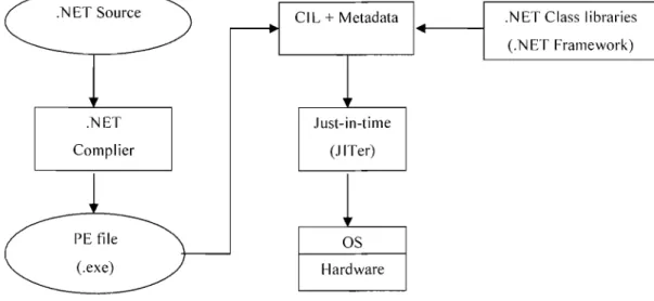
Metadata contain the information about compiled classes and sorne additional attributes. Metadata can be thought as the complementary descriptions for CIL instructions. For example, Metadata used for a method usually contain the information about the class name, the type of the return value and the type of the method parameter. The information ensures that the method can be invoked. The lIT compiler reads these Metadata during the .lIT compilation. In Figure 2, we show the basic process ofCLR (Common Language Runtime) .
. NET Source .NET Complier PEfiie (.exe) CI L + Metadata Just-in-time (J ITer) OS Hardware
Figure 2: Common Language Runtime
.NET Class libraries (.NET Framework)
The .NET compiler firstly translates a .NET programs to a PE (portable executable) file [23]. The PE file is a collection of CIL instructions and Metadata. When the PE file is executed, a .lIT compiler compiles CIL instructions and Metadata to native language
instructions. During the compilation, the JIT compiler refers to .NET class libraries. Finally, these new instructions can be executed on sorne special hardware environment with sorne special OS.
Introduction of SCIL processor
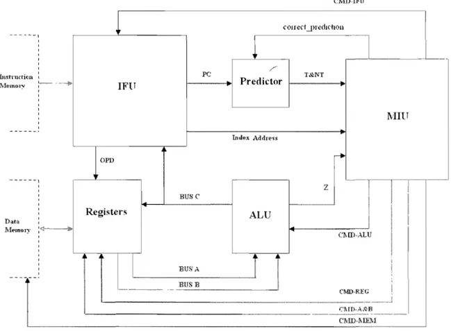
The SCIL processor is a synthesizable softcore processor which implements a subset of the CIL. lt is a little-endian processor. The processor supports 32 bits integer calculation, and it cannot execute floating-point operations. The processor does not support object-oriented concepts at present. ---~·--1 , , , , Instruction 1 TvlemOl-y , m",",,§~ Data IVI~lnory : CMIHFU
COI re,1 --.llrecilcholl
/ PC T&NT IFlT Predictor f - - - + I Index Addr." OPD z BUSC Registers ALU Cl\ID-ALU 1 BUf>A
J
BUS B ~--~~-'-- ' ' ' ' -, - - - ' - - - ' C~ID-REG CMD-l\IEl\iFigure 3: Block-diagram of SCIL processor
IVIIlT
In Figure 3, we present the block-diagram of the SCIL processor. The processor consists of the following functional units: Instruction Fetch Unit (IFU), Microinstruction Unit (MIU),
ALU, Predictor and Registers (local memory). The IFU fetches SOL instruction data From memory and then decodes the SCIL instruction code; the MIU picks out mÎcroinstructions and converts them to command signaIs; the ALU does the basic arithmetic operations and determÎnes whether the processor takes condition branches; the Predictor is a one-bit predictor with 128 different addresses for branch prediction; and the local memory consists of nine 32-bit registers. Furthermore, we can find three data buses (BUS A, BUS B and BUS C) and five command signal sets (CMO_A and B, CMD_ALU, CMD_REG, CMD_MEM, and CMD IFU) which control the operations ofdifferent units. In addition, the SCIL processor directly connects two BRAMs. One is as the instruction memory and the other is as the data memory.
Oufline of thesis
The remainder of the thesis is organized as follows. We will introduce the related work in nex! chapter. In chapter 3, we will discuss the CIL and the new language SCIL. Then in chapter 4, we will present the detailed SCIL processor architecture. We will explain the functions and characteristics of each unit of the processor. After that in chapter 5, wc will show sorne ex peri ment results, and we will compare and discuss the performance between the SCIL processor and the MicroBlaze processor. Finally, we will present the conclusion and future works in chapter 6.
Chapter 2
Related work
Currently most embedded processors, which target a specific programming language, focus on Java or JVM. These pro cess ors are usually called Java processors. In this chapter, we present several typical Java processors. We introduce three JVM based processors: SUN's picoJava processor, Co-Designed Java Virtual Machine processor developed by University of New Bunswick and Tanenbaum's IJVM processor. Moreover, we introduce the Lightfoot processor, which supports the instruction set interpreted from JVM. Furthermore, we introduce IBM System z Application Assist Processor (zAAP), which is unique Java processor used in large-scale commercial field.
picoJava processor
SUN's picoJava processor [12] may be the most famous Java processor although picoJava only appears in research papers and this processor is never released as a product by SUN. Now SUN provides the full Verilog code under an open source license [13]. The first version picoJava core, picoJava-I, was introduced in 1997.
Through an interpreter or through just-in-time (JIT) compilation, Java programs can be executed on a processor. However, both the interpretation and the .lIT compilation have their disadvantages. The nature of interpretation involves a time-consuming loop, which affects performance significantly. A JIT compiler can reach a high speed. However, because the compiler itself and compilation require large quantity of storage, it consumes much more memory, which is a precious resource in the embedded designs, than the interpretation. Therefore, SUN developed picoJava-I processor to create a processor to the Java environment which can eliminate the disadvantages of the two traditional execution ways. The picoJava-I is a small, configurable core designed to support the JVM. In Figure 4, we present the major function units of the picoJava-I. The shading parts indicate confi gurabi 1 ity.
1/0 bus and memory interface unit
32
~-Ir32
t
,
r
,<lnstrvêtion'
èache '"
(O'"16,Kby'tes)
PC and
trap
...
DÇita cache
32 -
~-control
(0-16 Kbytes)
Instruction
t
libuffer
...
r
Instruction
Execution
Data cache
decoding
-
..
control logic
controlier
and folding
~
32
~ 1 Al,1
'f
uL.
Stack cache unit
...
Integer unit
Floatinçf-point
/
....
(64 entries)
data path
idata :pâth
96
(r ,;. "
:
Figure 4: Block-diagram of picoJava-I processor [12]
The instruction cache is a direct-mapped cache with a line size of 8 bytes, while the data cache is a two ways, set-associative, write-back cache. Both of them can be conligured between 0 and 16 Kbytes. The picoJava-1 processor has a 64-entry stack cache which directly supports the JVM's stack based architecture. The stack cache is implemented as a register file and managed as a circular buffer with a pointer to the top of stack. The picoJava-I allows the option of including or excluding a floating-point unit. The pico.lava-I processor includes a RISC-style pipeline and a straightforward instruction set. It implements 341 different instructions. The processor implements simple Java bytecodes in circuitry and executes them in one to three cycles. For example, either integer addition or quick loads of object fields uses a circuitry directly. The picoJava-I implements sorne performance critical instructions, such as calling a procedure, by using microinstructions. Furthermore, for sorne complex instructions, such as creating the object or garbage
collection, the picoJava processor uses a trap to execute these instructions. One trap needs at least 16 cycles to complete executing. Besides, the picoJava-l processor does not have branch prediction logic. In Figure we present the picoJava-I processor's tour-stage pipeline.
1
Fetch
Decode
Execute
Write
and cache
back
Fetch 4-byte
Decode
Execute for
Write results
cache lines
up ta !\No
one or more
back into
into the
instructions
cycles
the operand
instruction
stack
buffer
Foldinglogic
Figure 5: PicoJava-I processor's four-stage pipeline [12]
'The picoJava-I processor can accelerate Java bytecode execution with a folding operation, which takes advantage of random single-cycle access to the stack cache. Example 2 shows that the processor can reduce one cycle to complete the stack operations by using folding operation. T
---...
LO~
T+LO 1i
~-~
T+LO i , . LO r-- LO ""LO ,--- LO LO.
1 (a) (b)Cycle 2: iadd Cycle 1: îload_O. iadd
The picoJava-I can be implemented minimal in about 440K gates [14]. Moreover, based on the experiments, the picoJava-I processor can reach 15 to 20 times faster th an a 486 with an interpreter at an equal clock rate, and five times faster than a Pentium with a .1 IT compiler at an equal clock rate.
Co-Designed
JVM
processor
The co-designed JVM processor [15J is developed by Kent from University of New Bunswick. This processor uses hardware/software partitions for a JVM within the context of a desktop workstation. The motivation of Kent is 10 relieve performance penalty caused by the translation from Java bytecodes to machine language. The co-designed JVM processor tries to leverage the combined benefits of hardware and software. Instead of 100% on hardware, Kent implemented only part of Java bytecodes on hardware.
The co-designed approach realizes a t'ully functional JVM comprised of both hardware and software support in a desktop workstation environment. The dedicated hardware, which is supported directly on the workstation mainboard, uses a FPGA tightly coupled with the workstation's general purpose processor through a PCI bus. The partitioning of the design between hardware and software is interesting. The processor uses overlap partitions between hardware and software instead of maintaining disjoint partitions which are normally used in co-designed systems. This partitioning is to relax the conditions to switch execution between hardware/software partitions. The instructions that can be implemented in the hardware partition are those that can be found in traditional processors such as stack manipulation, arithmetic operators and logic operations, comparison and branching, jllmp and return, as weil as data loading and storing. Most of accessed data structures, i.e. the method's bytecode, execlltion stack and local variables, are placed in the FPGA board memory. The constant pool and the heap reside in the PC's main memory. The software partition executes ail object-oriented bytecodes. It suppol1s many complex virtual machine functions, such as class loading and verification, garbage collection, exceptions, as well as memory management. For example, the instructions new, checkcast, and inslanceof are executed in software partition. The software partition is responsible for transferring data
during context switch between the hardware and software partitions. Furthermore, because some instructions are supported both in the hardware partition and in the software partition due to the overload partitioning, the software partition does a run-time decision to decide where these instructions are executed. The software partition decides during runtime which instruction sequences can be executed by the hardware. The whole system uses a single data bus and a controlline to realize a simple communication protocol between the two partitions. Once the hardware partition finishes execution, it signaIs the software using an interrupt. Then the software partition retrieves the current state of the virtual machine from hardware and continues execution.
The tests of small benchmarks on a simulator show performance gains by a factor of 6 to 11 compared with an interpreting JVM. (Kent does not introduce the machine used to run the software .JVM.) Kent does not show benchmark results on FPGA after implementing the processor. The hardware partition is coded in VHDL and the memory uses the memory space within the FPGA device. The interface with the PCI bus is Altera pci_mt64 MegaCore function. Through timing analysis, the maximum c\ock rate is 24 MHz. The design which implements the full partition (161 instructions) needs 37,756 logic elements with 64 entries instruction cache and data cache. When it uses 16 entries cache, the number of logic elements becomes 33,490.
Lightfoot processor
The 32-bit Lightfoot processor [16] is the product of Digital Communication Technologies. This processor can be used as a design solution of embedded system OEMs from a tiny memory footprint. It is a hybrid 8/32-bit processor based on Harvard architecture. This processor uses a 3-stage pipeline. The instruction memory is 8-bits wide while the data memory is 32-bits wide.
CPU Registers
ALU
Memory Arbiters Uni1ied Memory
Ihterface
Figure 6: Block-diagram of Lightfoot processor [16]
ln Figure 6, we show the key blocks of the Lightfoot processor. The shading part indicates configurability of the memory interface. The user can configure the size of memory and cache. The Control Unit is responsible for fetching, decoding and sequencing the execution of instructions in the processor. The ALU is a traditional 32-bit design. Besides the usual arithmetic and logic capabilities, it has a 32-bit balTel shifter and a 2-bit multiple step unit which can execute a 32x32 bit multiply in 16 cycles. Data stack holds temporary data. The return stack holds return addresses for subroutines. Its top-of-stack element is used as an index register to access program memory. Moreover, the return stack can be used as an auxiliary stack for programs. Both of the two stacks consist of a hardware part and a memory extension. The hardware part of the data stack consists of eight 32-bit on-chip registers while the hardware part of the return stack is four 32-bit registers. The processor has 256 words of register space. The sixteen addresses at the bottom of them are used as CUP registers su ch as the stack extension pointers, constant and parameter pool pointers. The other register space is for interfacing to system peripherals such as memory management unit. The processor supports the instruction set interpreted From JVM. The Lightfoot processor has three different instruction formats: soft bytecodes, non-returnable
instructions and 32 single-byte instructions: The Lightfoot processor implements the 128 soft bytecode instructions in low pro gram memory. When the processor needs to execute a soft byte code instruction, it branches to one location where the implementation of this soft bytecode resides. The processor needs one cycle to do this operation, and it pushes the address of the following instruction to the return stack. The 32 single-byte instructions can be folded with a return operation. The 32 single-byte instructions have a retulll bit. When this bit is set, the processor loads the value popped from the return stack to the program counter register. This mechanism implements a zero-overhead return feature orthe processor.
The frequency of the Lightfoot processor can reach 31 MHz on Spartan Il FPGA family and 40 MHz frequency on Virtex 11 FPGA families. It can be implemented with less than 30,000 gates for the conventional form.
IBM System z Application Assist Processor (zAAP)
The zAAP [21 ][35] is the tirst large-scale commercial Java processor. The zAAP is introduced by IBM in 2004, and available on IBM System z9 and zSeries z9901z890. (Because the zAAP is a commercial product of IBM, we can not tind the detailed architecture of this processor. We introduce the zAAP based on the introduction and presentation on IBM official website.) The objective of the zAAP is to integrate Java technology-based applications with mission-critical data and reduce infrastructure complexity for multi-tier applications.
The zAAP is not designed as an independent processor which works individually. USllally the zAAPs work as particular processors and do execute Java programs in IBM System z, IBM's mainframe computers. For example, IBM z990 has 10 CPs (conventional processor), 1 lCr (Integrated Coupling Facility), 2 IFLs (lntegrated Facility for Linux), and 3 zAAPs. The zAAPs execute Java programs in IBM JVM under control of z/OS [36], which is lBM's flagship mainframe operating system. When a Java program is to be execllted, z/OS
the left work units on standard processors. In Figure 7, we show how z/OS partitions Java works to zAAPs and general processors.
zAAP Technical Overview:
Z/OS
zAAP Partition
z/OS Logical Partition
Lo~~al ... '1
General CP Instructions,
.' ~. ~ -Wh;n-dÎ;patc-h~; - ; . : 'runs on GCPs it can '
". select non-JAVA and: :' JAVA work", '
, '
, l
When dispatcher':' runs on zAAP it can '
only select JAVA ' work
.~---_.----~
Figure 7: zAAP Technical Overview [35]
Bccause the zAAPs share many demands from general purpose processors, general purposc processors can be available for additional workloads. In Figure 8, we show a simple example. With the zAAPs, the system can reduce the standard CP capacity requirement for the application to 500 MIPS or a 50% reduction.
Consider a WebSphere Application that is transactional in nature and requires 1000 MIPS today on zSeries.
500 MIPB for WebSpnere App +
t",(lO MIPq now availalJle for addltional workloads
Figure 8: An example of zAAP [35]
The zAAP can execute z/ Architecture
™
instruction set architecture (JSA) [17][18][19]. The processor does not support ail manual operator controls such as PS W (Pro gram status word) Restart, Load or Load derivatives. Moreover, the zAAPs are supported by 1 SM middleware such as WebSphere, CICS and DB2.Tanenbaum' s lJVM processor
Tanenbaum's LTVM processor [1] is an implementation of micro-architecture. The IJVM processor can execute a subset of integer JVM (IJVM) on hardware. It implements only twenty-two different integer JVM instructions su ch as iload and Îsfore. Moreover, the processor does not natively support object-oriented concepts. The Tanenbaum's IJVM processor uses microinstructions and has a seven-stage pipeline. The processor has tlnee data buses and Il local registers. It do es not have prediction logic. In Figure 9, we show the basic architecture of the Tanenbaum's IJVM processor.
Figure 9: Tanenbaum's IJVM processor [1]
Additiona] Comments
We showed how the different Java processors implement an instruction set. Because implementing every instruction in circuitry needs too many hardware resources, there are few hardware processors which use this approach in practice. Instead, many processors, such as picoJava-I processor and Lightfoot processor, use the alternative approach where the processor implements simple instructions in circuitry and uses microinstructions to implement the complex instructions and native functions. This approach can reduce the amount of hardware resources and accelerate the execution of those instructions which are used frequently. Of course, the picoJava-I also uses software traps to implement sorne complex instructions. Using a number of traps may occur to reduce the performance of the processor because the picoJava-I needs minimum 16 cycles to complete a trap operation. The architecture of a processor with two or three different implementation approaches becomes complex.
Another solution we presented is co-design hardware/software approach used in Kent's processor. It partitions the whole implementation to hardware part and software part. Some instructions are implemented in hardware while others are executed in software. ln our opinion, this solution is very interesting and suggestive. However, the potential problem is the communication overhead. It is very difficult to predict how much time the processor uses to keep the communication while it executes sorne programs. Moreover, the raw speedup of the FPGA solution presented by Kent is under the condition that both the clock frequency and general-purpose processor have the same clock frequency. As we ail know, the clock frequency of a general-purpose processor is usually 20 to 50 faster than that of FPGA. Therefore, we doubt whether this co-design approach can be realized in practice.
Our SCIL processor adopts a simple approach: the whole instruction set is implemented by microinstructions. In fact, most of small processors use this approach, such as Tanenbaum's IJVM processor and Martin Schocberl's JOP [37]. During execution, every SCIL instruction is translated to an address and then mapped to one set of microinstructions. The processor can complete this translation in one pipeline stage without execution overheads. Moreover, since there is no instruction implemented in circuitry, the design can be implemented with minimal hardware. ln addition, because the architecture of the processor is relatively simple, the development period is shorter than with other approaches. Table
1
lists the Java processors we introduced.
Instruction set Clock Logic usages Implementation
frequencv approach
picoJava-1 JVM 440K gates Circuitry
processor M icroinstruction
Trap .~~ . . . g u n i JVM 24MHz 37K gates Co-Design proccssor
Lightfoot Interpreted from 40MHz 30K gates Circuitry
proccssor JVM M icroinstruction
Tancnbaurn's IJVM M icroinstruction
I.JVM proccssor
two processors have some similarities. For example, both of them use three data buses. However, there are also lots of ditferences between Tanenbaum's IJVM processor and the SCIL processor. First of ail, the instruction set our processor implements is SCIL instead of IJVM. The SCIL processor uses a new set of microinstructions, which is different l'rom other existing sets of microinstructions, to implements the SCIL instructions. Furthermore, we change a lot the architecture in order to make the SCIL processor fit the characteristics of the SCIL. For example, the SCIL processor has a different method to deal with branches because the SCIL use absolute address to represent branch address. Moreover, in order to reduce the number of suspending cycles, the SC IL adopts a predictor and the forwarding technique which are not used in the LTVM processor.
We introduced IBM's zAAP to show that the processors for a specific programmmg language have their commercial usages. As we can see, the zAAP has been used in large-scale commercial field. Furthermore, the zAAP gives one possible method to use the SCIL processor. IBM uses the zAAP as co-processors in lBM's mainframe computers to accelerate the execution of Java programs. Therefore in the future, it is very possible to use the processors for .NET languages in one system to improve the execution of .NET programs.
22
Chapter 3
CIL vs. SCIL
CIL: high level machine language
In our design, we do not directly use the CIL instructions for our processor. Instead, we create a new intermediate language, named SCIL (Simple CIL). By using a SCIL compiler (we will introduce it later), we translate a CIL pro gram to a SCIL program, and the two programs have the same signification. Then our SCIL processor can execute this SCIL program on FPGA. We use the SCIL to replace the CIL because it is hard to implement the CIL on hardware. The CIL is close to a machine language. It can be assembled into bytecode. At the same time, the CIL is an object language, and it supports object-oriented concepts. Therefore, we can think the CIL as a "high level machine language". In Example 3, we present a piece of CIL program to show its characteristics .
. class private auto ansi beforefieldinit Class1 extends [mscorlib]System.Object
{
. method private hidebysig static int32 zzz(int32 a) cil managed
{
.maxstack 2
.Iocals init ([0] int32 b,
[1] int32 CS$00000003$00000000) IL_OOOO: Idc.i4.6 IL 0001: stloc.O IL_0002: Idarg.O IL 0003: Idloc.O IL 0004: add IL 0005: stloc.O IL_0006: Idloc.O IL 0007: stloc.1 IL 0008: br.s IL OOOa IL OOOa: Idloc.1 IL OOOb: ret
} Il end of method Class1 ::zzz
.method private hidebysig static int32 Main(string[] args) cil managed
{
.entrypoint .maxstack 2
.Iocals init ([0] int32 x,
[1] int32 CS$00000003$00000000) IL_OOOO: Idc.i4.0
IL_0001: stloc.O
IL 0002: br.s IL_OOOd
IL_0006: cali int32 ConsoleApplieation1.Class1 ::zzz(int32) IL_OOOb: add IL_OOOe: stloe.O IL OOOd: Idloe.O IL OOOe: Ide.i4.s 100 IL 0010: blt.s IL 0004 IL_0012: Idloe.O IL_0013: stloc.1 IL_0014: br.s IL_0016 IL 0016: Idloe.1 IL_0017: ret
} Il end of method Class1 ::Main } Il end of class Class1
Example 3: The "high level machine language" CIL
As we can see, the CIL is close to a machine language because every CIL instruction can be expressed in form of bytecode instruction, such as "Idarg 0" or "br.s II~ _ OOOa". However we can find that the CIL is similar to high level languages such as C++ and Java. The CIL uses "return value + function name + parameter type" to declare one procedure, and uses one pair of "{" "}" to express the beginning and end of one procedure or class. The CIL supports object-oriented programming. Usually only high level languages have the se characteristics. As a resuIt, the se high Ievel language characteristics make the CIL much different from machine languages. A CIL program is more readable than a JVM program. However, it is a real nightmare for the hardware designers to construct the hardware solutions that implement the "machine language" CIL. It is difficult for one processor to know how to de al with some complex and tedious statements such as "private hidebysig static int32 zzz(int32 p) cil managed", or identify some characters like '{' and "". Therefore, we give up using the CIL as the machine language for our processor. We adopt an alternative approach: before loading CIL instructions into memory, we translate CIL instructions to the real machine instructions, and then implement these machine instructions on hardware. In this way, we can avoid using the complex CIL statements and sllccess in executing the CIL program on hardware. Furthermore, we can reduce significantly the total amount of hardware resources and shorten the development period.
SCI
L:
Simplifying CIL
The SCIL is designed for our processor, and it is the real machine language for the processor. The basic idea of generating SCIL instructions is to simplify the CIL. The SCIL has no Metadata, and only consists of bytecode instructions. The SCIL is equivalent to a subset of the CIL. Nowadays it only supports 32 bits signed integer, and does not support
tloating-point operations and object-oriented concepts.
There exist a lot of differences between the CIL and the SCJL. First of ail, the instruction codes of the SCIL are completely different from their prototypes, the instruction codes of the CIL. We redefine all instruction codes of SCIL instructions. For example, the instruction code of add is Ox58 in CIL when the new instruction code is OxOI in SCJL. Secondly, for some SCIL instructions, although they still own the same names as CIL instructions, their instruction operands may represent different signification. Taking the instruction cali for example, the instruction operand of cali in CIL represents the name of invoking procedure, however the instruction operand of cali in SCIL represents the branch address of invoking procedure. Thirdly, because usually one SCIL instruction corresponds to several CIL instructions, the SCIL has much less instructions than the CIL has. (We will introduce these differences in following sections.)
Metadata
The SCIL has no Metadata any more. lt is not easy for a processor to deal with Metadata because lIsually Metadata have various forms and different parameters. We remove Metadata by using three ways. Firstly, we directly delete some Metadata. Because now the SCIL is not an object language, many Metadata are not useful any more. Therefore, although we throw away these Metadata to garbage, we do not change the signification of the whole program. For example, the Metadata .class, this Metadata is useful for the CIL to declare the beginning of one class definition. However, the SCIL does not have the concept of c1ass. Hence, this Metadata becomes not useful, and we can delete it without hesitation.
The second way of dealing with Metadata is to remove the Metadata but still complete this Metadata's job. For example, the Metadata .enlrypoinf represents which procedure is the main procedure in the program. For the SCIL, there is not one instruction
\
which functions as to indicate the position of the main procedure. Alternatively, we define that ail SClL programs are executed from the first instruction, the first line of the source code. Then we move the procedures, which contains the Metadata .entrypoinl in CIL. to the beginning of the SCIL programs. In this way, we can delete the Metadata .entrypoint when the SCIL programs still know the position ofthe main procedure.
The third way is that we use SCIL instructions to replace some Metadata. For example, we replace the Metadata .locals with the SCIL instruction local opd. We show an example for Metadata .local.~' .
. Iocals init ([0] int32 a, [1] int32 b)
ln this example, the Metadata .locals expresses that there are two local variables a and h in the current procedure. For the SCIL, it is not necessary to remember the name of variables because the SCIL al ways use a number to represent a local variable. Instead, the number of local variables is very useful for the SCIL. For the above example, the SCIL will name variable li as 0111 variable b as 1 si variable. Therefore it is necessary to keep the number of variables frol11 the Metadata .locals. We use a SCIL instruction local opd, where opd
represents the number of variables, to replace the Metadata .locals. Therefore, we can replace the Metadata .locals in the above example with the SCIL instruction local 2. In this way, the SCIL can keep the information the CIL Metadata contain by only using SCIL instructions.
Regrouping Instructions
We do some simplifications for CIL instructions while translating them to SCIL instructions. We reduce the number of CIL instructions. Usually, several CfL instructions correspond to only one SCIL instruction. For example, loading an integer value to the top of stack is an often-used operation in the CIL, and the CIL has a series of instructions to do loading an integer with different value. (See Table 2)
26
CIL instruction Comment
Idc.i4.m1 Load integer -1 to the top of stack Idc.i4.0 Load integer 0 to the top of stack Idc.i4.1 Load integer 1 to the top of stack Idc.i4.2 Load integer 2 to the top of stack Idc.i4.3 Load integer 3 to the top of stack Idc.i4.4 Load integer 4 to the top of stack Idc.i4.5 Load integer 5 to the top of stack Idc.i4.6 Load integer 6 to the top of stack Idc.i4.7 Load integer 7 to the top of stack Idc.i4.8 Load integer 8 to the top of stack Idc.i4.s opd Load integer opd to the top of stack
Table 2: Various CIL loading instructions
J f we kept this series of loading instructions without any change, our processor should have implemented them as ten different instructions. Now the SCIL only uses one instruction,
louds opd, where opd represents the value of the integer loaded, to replace aU these ten CIL loading instructions. For example, the CIL instruction Ide. i4. m 1 can be represented by the SCIL instruction loads -1; and the CIL instruction Idc.i4.(J can be represented by the SC[L instruction louds (J. As a result, our processor can only use almost 1/1 0 hardware resources which are needed to implement ail ten loading instructions. Such a simplification a[so refers to the CIL instructions such as ldarg, ldloc and st/oc.
[n fact, if the processor can implement some instructions 1\1 circuitry, the speed of execution may be improved. For example, the SCIL can use three instructions to represent the various CIL loading instructions: louds (J, louds 1 and louds opd, and the processor implements louds (J and louds J in circuitry. As a result, because the first two instructions are used frequently, the processor can accelerate execution of programs. Moreover, .iust implementing two instructions in circuitry do not need lots of additional hardware resources. However, the probIem is how many and which instructions could be
implemented in circuitry. Furthermore, the architectural of the processor with many circuitries becomes more complex th an that of our current processor. We think maybe the SCIL processor could implement part of instructions in circuitry in future woks.
Absolute address
When translating CIL branch instructions such as br.s, bge and cali to SCIL instructions,
we change the instruction operands of these CIL branch instructions. We use the absolute branch addresses as the instruction operands of the SCIL instructions.
The .rIT compiIers ailocate memory for CIL instructions at application run time. (The different .lIT compilers may use different methods to allocate memory address. We use the document Microsoft's .NET Framework Developer's Guide [24] as our reference.) Before CIL instructions are executed, ail CIL instructions are kept in the PE file. When the se CIL instructions are executed, one .NET Framework .Ill' compiler is responsible to convert them to native code. During the execution, the .lIT compiler does not convert ail CIL instructions to native code at one time. The compiler does not load one procedure (or method) until this procedure (or method) is needed. When it is the first time to invoke one procedure, the .lIT compiler converts this block of instructions, ail of the CIL code for this procedure, to native code. Then the lIT compiler locals the native code in memory. Subsequent calls of the compiled procedure are proceed directly to the native code that was previously generated. The benefit is that some code which never gets invoked during the execution is not loaded in memory. Rather than using time and memory to convert ail the CI L to native code, the .lIT compiler only converts the CIL needed during execution and stores the resulting native code.
In Example 4, we show a piece of CIL program. For each CIL instruction, it has a label like
IL_xxxx, which are generated by the CIL compiler. In this example, we suppose that the first
instruction Ide. ;4. 6 is the beginning of one procedure, and ail instructions are in the same procedure. Wh en this procedure is invoked, the .lIT compiler converts ail CIL instructions in this procedure to native code, and loads them to memory. The nLllllbers in parentheses before each CIL instruction in the example represents the memory address, which is al\ocated by the JIT compiler.
(Ox0105) (Ox0106) (Ox0107) (Ox0108) (Ox0109) (Ox010A) (Ox010B) (Ox010C) (Ox010D) IL_OOOO: Idc.i4.6 IL 0001: stloc.O IL_0002: Idarg.O IL_0003: Idloc.O IL_0004: add IL_0005: stloc.O IL_0006: Idloc.O IL_0007: stloc.1 IL_0008: br.s IL 0002
Example 4: Branch instruction in CIL
The instruction br.s IL _ 0002 is a branch instruction, which represent that the program goes
to the label IL_0002 when the first element is bigger than the second. The label IL_0002 in
the branch instruction does not represent the absolute bran ch address but the relative displacement to the beginning of current procedure. Therefore, in order to obtain the target branch address, the compiler has to do a calculation based on this relative displacement. It adds the displacement (lL_0002 - ILOOOO = 2) to the first instruction's memory address of the CUITent procedure (OxOI05), and then the compiler can obtain the branch address (OxOI07).
Unlike the CIL, the SClL uses static allocation to allocate SCIL instructions in memory. Ail SCIL instruction will be loaded in memory whatever they are executed or not. Before being loaded in memory, we can know the memory address of every SCIL instruction. The first instruction of the main procedure always occupies the memory address OxOOOO. The SClL compiler calculates the address of every instruction in memory. Clearly it is not a Just-In-Time compilation. However, this kind of memory allocation can reduce the workload of the SCIL processor because such an expression enables the processor to avoid branch address calculation on the f1y. When the processor obtains an SCIL instruction, it can immediately know where the next instruction in memory. Hence the processor does not need any operations to calculate memory addresses.
The SCIL uses the absolute address to represent bran ch addresses. When the SCIL compiler translates CIL instructions to SCIL instructions, it calculates the branch address for ail bran ch instructions. Then the SC IL branch instructions use bran ch addresses as their
instruction operands. In Example 5, we show the SCIL instructions equivalent to the CIL instructions presented in Example 4. We suppose that the address in parentheses is the memory address in instruction memory for the SCIL processor. The last instruction br Ox002E is equivalent to the instruction br.s IL_0002 in Example 4. Now the instruction operand Ox002E represents the branch address. When the processor executes this instruction, the processor knows the memory address of the next instruction is Ox002E.
(Ox0029) (Ox002C) (Ox002E) (Ox0030) (Ox0032) (Ox0033) (Ox0035) (Ox0037) (Ox0039) loads 6 stloc Idarg Idloc add
o
o
o
stloc 0 Idloc 0 stloc 1 br Ox002EExample 5: Branch instruction in SCIL
For the CIL, the call instruction includes the invoking procedure name, the type of parameters and the type of return value. When the .lIT compiler executes a call instruction, the compiler searches the list of procedures to check the procedure name, the type of parameters and the type ofreturn value. Then the lIT compiler examines the CIL instruction and Metadata to determine whether the code Îs type safe, which means a reference to a type is strictly compatible with the type being referenced. Only appropriately defined calling operations can invoke a procedure.
In Example 6, we show a piece of CIL program. We also add the memory address allocated by the .lIT compiler for each instruction in parenthesis. We suppose that the firs1 part of instructions (the first five instructions) is in the main procedure, and the second part of instructions is in another procedure named zzz. In the main procedure, there is a cali instruction, cali int32 Test.TestClass::zzz(int32), which invokes the procedure zzz. We can see that the cali instruction provides lots of infonnation to the lIT compiler.
(Ox0120) IL_OOOe: Idloc.1 (Ox0121) IL_OOOt: stloc.2 (Ox0122) IL_0010: Idloc.2
(Ox0123) IL_0011: cali int32 Test.TestClass::zzz(int32) (Ox0125) IL_0016: stloc.2
.method private hidebysig static int32 zzz(int32 p) cil managed
(Ox0307) IL_OOOO: Idarg.O (Ox0308) IL_0001: Idloc.O (Ox0309) IL_0002: add
Example 6: Procedure cali in CIL
For the SCIL, the SCIL compiler does the job of searching the target procedure. Unlike the .rIT compiler searching the invoking procedures during the execution, the SCIL compiler finds out the position of the invoking procedures before SCIL instructions are loaded in memory. Furthermore the SCIL uses the branch address as the instruction operand of the SCIL instruction calI. The branch address is the memory address of the first instruction in the invoking procedure. In Example 7, we show the SCIL instructions equivalent to the CIL instructions presented in Example 6. We suppose that the address in parentheses is the memory address in instruction memory for the SCIL processor. The new cali instruction becollles call Ox0027. The ope rand Ox0027 is the bran ch address which is the Illelllory address of the first instruction in the procedure zzz.
(OxOOO2) loads 1 (OxOOO5) stloc 1 (OxOOO7) loads 2 (OxOOO9) cali OxOO27 (OxOOOS) stloc 2
(OxOO27) local 2 (OxOO2E) Idarg 0 (OxOO30) Idloc 0 (OxOO32) add
Example 7: Procedure cali in CIL
By using absolute addresses to represent branch addresses, ail branch instructions can tell the processor where the next instruction in the instruction memory. The processor does not need calculate branch addresses during the execution, and the processor can hence obtain l'aster speed than with ordinary CIL. However, the method of absolute address can only used in simple embedded system designs. If we make the processor support object-oriented concept, we still need to use dynamic branch calculation. At this time, the processor has to know the position of instructions in sorne c1ass instantiations, and the branch addresses are different for the same branch instructions.
Three types of SCIL instructions
Based on the length of bits which one SC IL instruction requires, we divided ail SClL instructions into three types. The Type 1 SCIL instruction occupies 8 bits and does not have instruction operand. It needs one word (8 bits per word) in the instruction l11emory for the SCIL processor. The Type 2 SCIL instruction needs 16 bits and two words in the memory. The first 8 bits represent the instruction code, and the rest bits represent the 8 bit signed integer operand. The Type 3 SCIL instruction demands 24 bits and three words in memory. The first 8 bits are for instruction code and the others are as the instruction operand, a signed 16 bits integer. Furthermore, in order to discriminate the types of SCIL instructions easily, we use the first two bits of instruction code to identify the different types. The Type 1 instructions begin with two bits "00"; the Type 2 instructions begin with "01"; and the first bit of the Type 3 instruction is '']''. In Table 3, we show three examples for the three types SCIL instructions, and we also show them in binary form when they are loaded in the instruction memory.
Examples Binary form in memory
i _ ..
~._._---~
add 00000010i Type 2 Idarg 2 01000101
![Figure 1: Xilinx MicroBlaze [20]](https://thumb-eu.123doks.com/thumbv2/123doknet/12396057.331629/16.916.207.738.152.504/figure-xilinx-microblaze.webp)
![Figure 4: Block-diagram of picoJava-I processor [12]](https://thumb-eu.123doks.com/thumbv2/123doknet/12396057.331629/23.916.183.812.132.633/figure-block-diagram-picojava-i-processor.webp)
![Figure 5: PicoJava-I processor's four-stage pipeline [12]](https://thumb-eu.123doks.com/thumbv2/123doknet/12396057.331629/24.916.172.830.281.560/figure-picojava-processor-four-stage-pipeline.webp)
![Figure 6: Block-diagram of Lightfoot processor [16]](https://thumb-eu.123doks.com/thumbv2/123doknet/12396057.331629/27.918.227.783.128.498/figure-block-diagram-lightfoot-processor.webp)
![Figure 7: zAAP Technical Overview [35]](https://thumb-eu.123doks.com/thumbv2/123doknet/12396057.331629/29.916.185.787.216.641/figure-zaap-technical-overview.webp)
![Figure 8: An example of zAAP [35]](https://thumb-eu.123doks.com/thumbv2/123doknet/12396057.331629/30.916.231.780.141.484/figure-example-zaap.webp)
![Figure 9: Tanenbaum's IJVM processor [1]](https://thumb-eu.123doks.com/thumbv2/123doknet/12396057.331629/31.916.188.794.117.536/figure-tanenbaum-s-ijvm-processor.webp)
